 | –≠–ª–µ–∫—Ç—Ä–æ–Ω–Ω—ã–π –∫–æ–º–ø–æ–Ω–µ–Ω—Ç: OP471G | –°–∫–∞—á–∞—Ç—å:  PDF PDF  ZIP ZIP |
OP471 Data sheet
REV. A
Information furnished by Analog Devices is believed to be accurate and
reliable. However, no responsibility is assumed by Analog Devices for its
use, nor for any infringements of patents or other rights of third parties that
may result from its use. No license is granted by implication or otherwise
under any patent or patent rights of Analog Devices.
a
OP471
One Technology Way, P.O. Box 9106, Norwood, MA 02062-9106, U.S.A.
Tel: 781/329-4700
www.analog.com
Fax: 781/326-8703
© Analog Devices, Inc., 2002
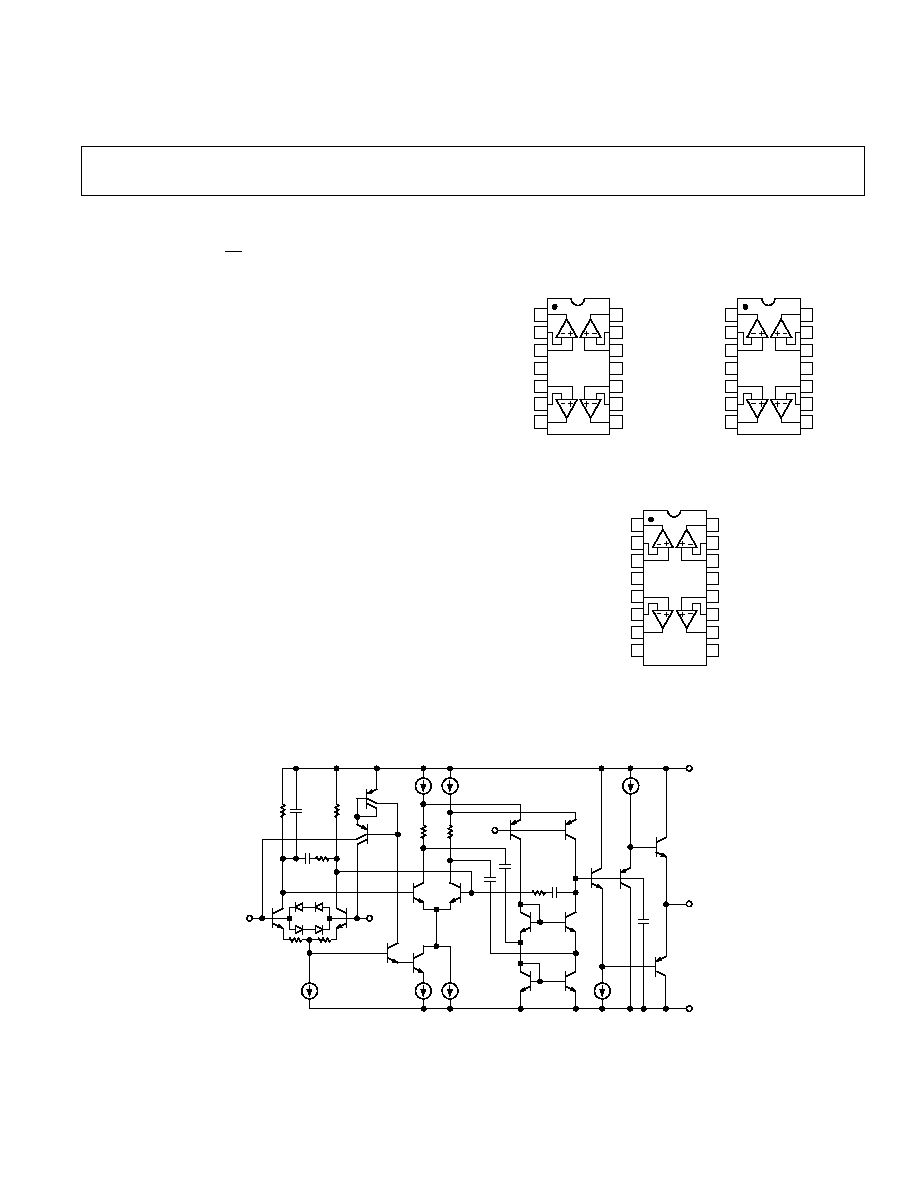
14-Lead
Hermetic Dip
(Y-Suffix)
14
13
12
11
10
9
8
1
2
3
4
5
6
7
OUT A
≠IN A
+IN A
V+
+IN B
≠IN B
OUT B
OUT D
≠IN D
+IN D
V≠
+IN C
≠IN C
OUT C
OP471
16-Lead SOIC
(S-Suffix)
16
15
14
13
12
11
10
9
1
2
3
4
5
6
7
8
NC = NO CONNECT
OUT A
OUT D
OP471
≠IN A
≠IN D
+IN A
+IN D
V+
V≠
+IN B
+IN C
≠IN B
≠IN C
OUT B
OUT C
NC
NC
High Speed, Low Noise Quad
Operational Amplifier
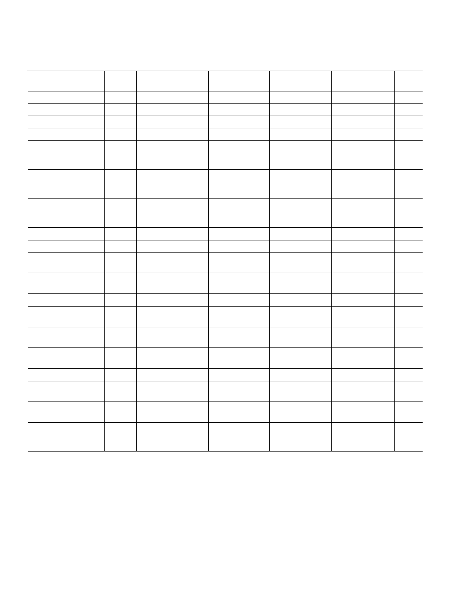
≠IN
+IN
BIAS
V≠
V+
OUT
Figure 1. Simplified Schematic
FEATURES
Excellent Speed: 8 V/ s Typ
Low Noise: 11 nV/
˜Hz @ 1 kHz Max
Unity-Gain Stable
High Gain Bandwidth: 6.5 MHz Typ
Low Input Offset Voltage: 0.8 mV Max
Low Offset Voltage Drift: 4 V/ C Max
High Gain: 500 V/mV Min
Outstanding CMR: 105 dB Min
Industry Standard Quad Pinouts
GENERAL DESCRIPTION
The OP471 is a monolithic quad op amp featuring low noise,
11 nV/
˜Hz Max @ 1 kHz, excellent speed, 8 V/ms typical, a
gain bandwidth of 6.5 MHz, and unity-gain stability.
The OP471 has an input offset voltage under 0.8 mV and an
input offset voltage drift below 4
mV/C, guaranteed over the full
military temperature range. Open-loop gain of the OP471 is over
500,000 into a 10 k
W load ensuring outstanding gain accuracy
and linearity. The input bias current is under 25 nA limiting
errors due to signal source resistance. The OP471's CMR of
over 105 dB and PSRR of under 5.6
mV/V significantly reduce
errors caused by ground noise and power supply fluctuations.
The OP471 offers excellent amplifier matching which is important
for applications such as multiple gain blocks, low-noise instru-
mentation amplifiers, quad buffers and low-noise active filters.
The OP471 conforms to the industry standard 14-lead DIP
pinout. It is pin-compatible with the LM148/LM149, HA4741,
RM4156, MC33074, TL084 and TL074 quad op amps and can
be used to upgrade systems using these devices.
For applications requiring even lower voltage noise the OP470
with a voltage density of 5 nV/
˜Hz Max @ 1 kHz is recommended.
PIN CONFIGURATIONS
14-Lead
Plastic Dip
(P-Suffix)
14
13
12
11
10
9
8
1
2
3
4
5
6
7
OUT A
≠IN A
+IN A
V+
+IN B
≠IN B
OUT B
OUT D
≠IN D
+IN D
V≠
+IN C
≠IN C
OUT C
OP471
REV. A
≠2≠
OP471≠SPECIFICATIONS
OP471E
OP471F
OP471G
Parameter
Symbol
Conditions
Min
Typ Max
Min Typ Max
Min Typ Max
Unit
Input Offset Voltage
V
OS
0.25 0.8
0.5
1.5
1.0
1.8
mV
Input Offset Current
I
OS
V
CM
= 0 V
4
10
7
20
12
30
nA
Input Bias Current
I
B
V
CM
= 0 V
7
25
15
50
25
60
nA
Input Noise Voltage
1
e
n
p-p
0.1 Hz to 10 Hz
250
500
250
500
250
500
nV p≠p
Input Noise
e
n
f
O
= 10 Hz
9
16
9
16
9
16
nV/
˜Hz
Voltage Density
2
f
O
= 100 Hz
7
12
7
12
7
12
nV/
˜Hz
f
O
=
1 kHz
6.5
11
6.5
11
6.5
11
nV/
˜Hz
Input Noise
i
n
f
O
= 10 Hz
1.7
1.7
1.7
pA
˜Hz
Current Density
f
O
= 100 Hz
0.7
0.7
0 7
pA
˜Hz
f
O
= 1 kHz
0.4
0.4
0.4
pA
˜Hz
Large-Signal
A
VO
V =
±10 V
Voltage Gain
R
L
= 10 k
W
500
700
300
500
300
500
V/mV
R
L
= 2 k
W
350
550
175
275
175
275
V/mV
Input Voltage Range
3
IVR
±11 ±12
±11 ±12
±11 ±12
V
Output Voltage Swing
V
O
R
L
2 k
W
±12 ±13
±12 ±13
±12 ±13
V
Common-Mode
CMR
V
CM
=
±11 V
105
120
95
115
95
115
dB
Rejection
Power Supply
PSRR
V
S
= 4.5 V to 18 V
1
5.6
5.6
17.8
5.6
17.8
mV/V
Rejection Ratio
Slew Rate
SR
6.5
8
6.5
8
6.5
8
V/
ms
Supply Current
I
SY
No Load
9.2
11
9.2
11
9.2
11
mA
(All Amplifiers)
Gain Bandwidth
GBW
Av = 10
6.5
6.5
6.5
MHz
Product
Channel Separation
1
CS
V
O
= 20 V p-p
125
150
125
150
125
150
dB
f
O
= 10 Hz
Input Capacitance
C
IN
2.6
2.6
2.6
pF
Input Resistance
R
IN
1.1
1.1
1.1
M
W
Differential-Mode
Input Resistance
R
INCM
11
11
11
G
W
Common-Mode
Settling Time
t
S
A
V
= 1
To 0.1%
4.5
4.5
4.5
ms
To 0.01 %
7.5
7.5
7.5
ms
NOTES
1
Guaranteed but not 100% tested.
2
Sample tested.
3
Guaranteed by CMR test.
ELECTRICAL CHARACTERISTICS
(@ V
S
= 15 V, T
A
= 25 C, unless otherwise noted.)
REV. A
≠3≠
OP471
OP471E
OP471F
OP471G
Parameter
Symbol
Conditions
Min
Typ Max
Min Typ Max
Min Typ Max
Unit
Input Offset Voltage
V
OS
0.3
1.1
0.6
2.0
1.2
2.5
mV
Average Input
TCV
OS
1
4
2
7
4
mV/C
Offset Voltage Drift
Input Offset Current
los
V
CM
= 0 V
5
20
8
40
20
50
nA
Input Bias Current
I
B
V
CM
= 0 V
13
50
25
70
40
75
nA
Large-Signal
V
O
=
±10 V
Voltage Gain
Avo
R
L
= 10 k
W
375
600
200
400
200
400
V/mV
R
L
= 2 k
W
250
400
125
200
125
200
Input Voltage Range
*
IVR
±11 ±12
±11 ±12
±11 ±12
V
Output Voltage Swing
V
O
R
L
2 k
W
±12 ±13
±12 ±13
±12 ±13
V
Common-Mode
CMR
V
CM
=
±11 V
100
115
90
110
90
110
dB
Rejection
Power Supply
PSRR
V
S
=
±4.5 V to ±18 V
3.2
10
18
31.6
18
31.6
mV/V
Rejection Ratio
Supply Current
(All Amplifiers)
I
SY
No Load
9.3
11
9.3
11
9.3
11
mA
*Guaranteed by CMR test.
ABSOLUTE MAXIMUM RATINGS
1
Supply Voltage . . . . . . . . . . . . . . . . . . . . . . . . . . . . . . . .
±18 V
Differential Input Voltage
2
. . . . . . . . . . . . . . . . . . . . . .
±1.0 V
Differential Input Current
2
. . . . . . . . . . . . . . . . . . . .
±25 mW
Input Voltage . . . . . . . . . . . . . . . . . . . . . . . . . . Supply Voltage
Output Short-Circuit Duration . . . . . . . . . . . . . . . Continuous
Storage Temperature Range
P, Y-Package . . . . . . . . . . . . . . . . . . . . . . ≠65
C to +150C
Lead Temperature Range (Soldering, 60 sec) . . . . . . . . 300
C
Junction Temperature (T
i
) . . . . . . . . . . . . . ≠65
C to +150C
Operating Temperature Range
OP471E, OP471F . . . . . . . . . . . . . . . . . . . ≠25
C to +85C
OP471G . . . . . . . . . . . . . . . . . . . . . . . . . . . ≠40
C to +85C
NOTES
1
Absolute Maximum Ratings apply to packaged parts, unless otherwise noted.
2
The OP471's inputs are protected by back-to-back diodes. Current limiting
resistors are not used in order to achieve low noise performance. If differential
voltage exceeds
±1.0 V, the input current should be limited to ±25 mA.
Package Type
JA
*
JC
Unit
14-Lead Hermetic DIP(Y)
94
10
C/W
14-Lead Plastic DIP(P)
76
33
C/W
16-Lead SOIC (S)
88
23
C/W
*
JA
is specified for worst-case mounting conditions, i.e.,
JA
is specified for device
in socket for TO, CERDIP, PDIP packages;
JA
is specified for device soldered to
printed circuit board for SO packages.
CAUTION
ESD (electrostatic discharge) sensitive device. Electrostatic charges as high as 4000 V readily
accumulate on the human body and test equipment and can discharge without detection. Although
the OP471 features proprietary ESD protection circuitry, permanent damage may occur on
devices subjected to high-energy electrostatic discharges. Therefore, proper ESD precautions
are recommended to avoid performance degradation or loss of functionality.
WARNING!
ESD SENSITIVE DEVICE
ORDERING GUIDE
T
A
= 25
C Package Options
Operating
V
OS
MAX
Temperature
(
mV)
14-Lead CERDIP Plastic
Range
800
OP471EY
IND
1,500
OP471FY
*
IND
1,800
OP471GP
XIND
1,800
OP471GS
XIND
*Not for new design. Obsolete April 2002.
For military processed devices, please refer to the standard
microcircuit drawing (SMD) available at
www.dscc.dla.mil/programs/milspec/default.asp
5962-88565022A - OP471ARCMDA
5962-88565023A - OP471ATCMDA
5962-8856502CA - OP471AYMDA
ELECTRICAL CHARACTERISTICS
(V
s
=
±15 V, ≠25 C
£
T
A
£ 85 C for OP471E/F, ≠40 C
£
T
A
£ 85 for OP471G,
unless otherwise noted.)
REV. A
OP471
≠4≠
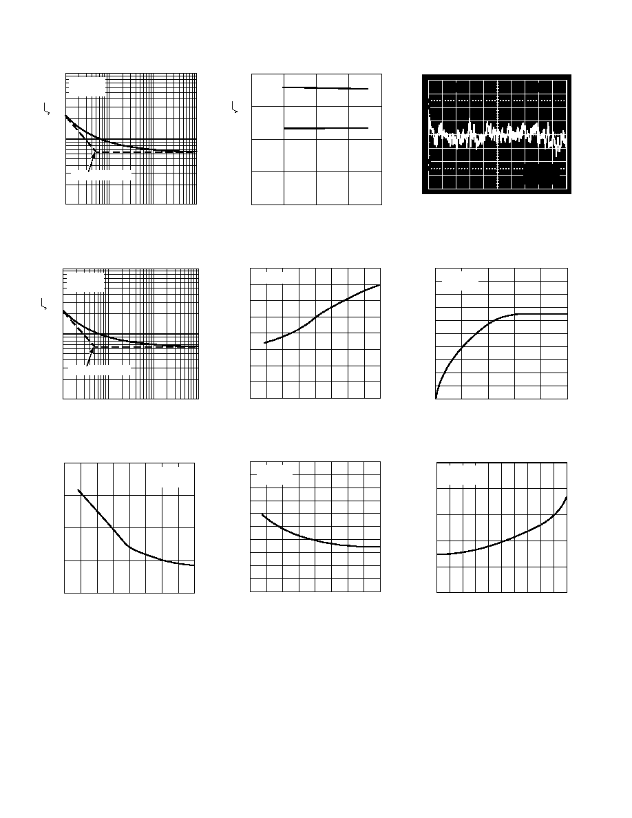
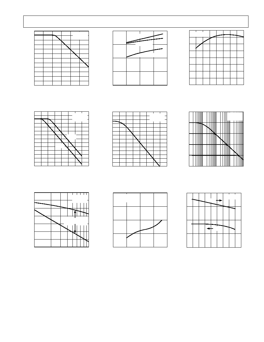
FREQUENCY ≠ Hz
100
1
40
5
4
3
2
1
10
100
1k
VO
LTA
G
E
N
OISE ≠ nV/ Hz
T
A
= 25 C
V
S
= 15V
30
20
10
I/F CORNER = 5Hz
TPC 1. Voltage Noise Density
vs. Frequency
FREQUENCY ≠ Hz
100
1
40
5
4
3
2
1
10
100
1k
VO
LTA
G
E
N
OISE ≠ nV/ Hz
T
A
= 25 C
V
S
= 15V
30
20
10
I/F CORNER = 5Hz
TPC 4. Current Noise Density
vs. Frequency
TEMPERATURE ≠ C
INPUT BIAS CURRENT ≠ nA
≠75
20
15
10
5
0
≠50
≠25
0
25
50
75
100
125
V
S
= 15V
V
CM
= 0V
TPC 7. Input Bias Current vs.
Temperature
SUPPLY VOLTAGE ≠ V
VO
LTA
G
E
N
OISE ≠ nV/ Hz
10
8
2
0
5
20
10
15
6
4
T
A
= 25 C
AT 10Hz
AT 1kHz
TPC 2. Voltage Noise Density
vs. Supply Voltage
TEMPERATURE ≠ C
INPUT OFFSET
V
O
L
T
A
GE ≠
V
400
≠75
V
S
= 15V
200
300
100
0
≠50
≠25
0
25
50
75
100
125
TPC 5. Input Offset Voltage vs.
Temperature
TEMPERATURE ≠ C
INPUT OFFSET CURRENT ≠ nA
10
≠75 ≠50
≠25
0
25
50
75
100 125
9
8
7
6
5
4
3
2
1
0
V
S
= 15V
V
CM
= 0V
TPC 8. Input Offset Current vs.
Temperature
5mV
1s
0
2
4
6
8
10
TIME ≠ Seconds
NOISE V
O
L
T
A
GE
≠
100nV/DIV
10
0%
100
90
T
A
= 25 C
V
S
= 15V
TPC 3. 0.1 Hz to 10 Hz Noise
TIME ≠ Minutes
CHANGE IN OFFSET
V
O
L
T
A
GE ≠
V
20
0
T
A
= 25 C
V
S
= 15V
18
16
14
12
10
8
6
4
2
0
1
2
3
4
5
TPC 6. Warm-Up Offset
Voltage Drift
COMMON-MODE VOLTAGE ≠ V
INPUT BIAS CURRENT ≠ nA
10
≠12.5
T
A
= 25 C
V
S
= 15V
9
8
7
6
5
≠7.5
≠2.5
2.5
7.5
12.5
TPC 9. Input Bias Current vs.
Common-Mode Voltage
≠Typical Performance Characteristics
REV. A
≠5≠
OP471
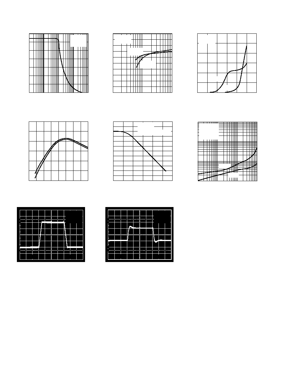
FREQUENCY ≠ Hz
CMR ≠ dB
130
1
T
A
= 25 C
V
S
= 15V
120
110
100
90
80
70
60
50
30
40
20
10
10
100
1k
10k
100k
1M
TPC 10. CMR vs. Frequency
FREQUENCY ≠ Hz
PSR ≠ dB
140
1
120
100
80
60
40
20
0
10
100
1k
10k 100k 1M 10M 100M
130
110
90
70
50
30
10
T
A
= 25 C
V
S
= 15V
≠PSR
+PSR
TPC 13. PSR vs. Frequency
FREQUENCY ≠ MHz
OPEN-LOOP GAIN ≠ dB
25
1
20
15
10
5
0
2
3
4
5
≠5
≠10
6 7 8 9 10
T
A
= 25 C
V
S
= 15V
80
100
120
140
160
180
200
220
PHASE SHIFT ≠ Degrees
PHASE
GAIN
PHASE MARGIN
= 57
TPC 16. Open-Loop Gain,
Phase Shift vs. Frequency
SUPPLY VOLTAGE ≠ V
TO
TA
L SUPPL
Y CURRENT ≠ mA
10
8
2
0
5
20
10
15
6
4
T
A
= +25 C
T
A
= +125 C
T
A
= ≠55 C
TPC 11. Total Supply Current
vs. Supply Voltage
FREQUENCY ≠ Hz
OPEN-LOOP GAIN ≠ dB
140
1
120
100
80
60
40
20
0
10
100
1k
10k 100k 1M 10M 100M
130
110
90
70
50
30
10
T
A
= 25 C
V
S
= 15V
TPC 14. Open-Loop Gain vs. Frequency
SUPPLY VOLTAGE ≠ V
OPEN-LOOP GAIN ≠
V/mV
2000
0
T
A
= 25 C
R
L
= 10k
1500
1000
500
0
5
10
15
20
TPC 17. Open-Loop Gain vs.
Supply Voltage
TEMPERATURE ≠ C
TO
TA
L SUPPL
Y CURRENT ≠ mA
10
≠75
≠50
≠25
0
25
50
75
100 125
9
8
7
6
5
4
3
2
V
S
= 15V
TPC 12. Total Supply Current
vs. Temperature
FREQUENCY ≠ Hz
CLOSED-LOOP GAIN ≠ dB
80
1k
60
40
20
0
≠20
10k
100k
1M
10M
T
A
= 25 C
V
S
= 15V
TPC 15. Closed-Loop Gain
vs. Frequency
TEMPERATURE ≠ C
PHASE MARGIN ≠ Degrees
80
≠75 ≠50 ≠25
0
25
50
75 100 125 150
70
60
50
40
8
6
4
2
0
GAIN-B
AND
WIDTH PR
ODUCT ≠ MHz
V
S
= 15V
GBW
TPC 18. Gain-Bandwidth Product,
Phase Margin vs. Temperature
REV. A
OP471
≠6≠
FREQUENCY ≠ Hz
PEAK-T
O-PEAK AMPLITUDE ≠
V
28
1k
24
20
16
12
8
10k
100k
1M
10M
4
0
T
A
= 25 C
V
S
= 15V
THD = 1%
TPC 19. Maximum Output Swing
vs. Frequency
TEMPERATURE ≠ C
SLEW RA
TE ≠
V/
s
9.0
≠75
8.5
8.0
7.5
7.0
6.5
≠50 ≠25
0
25
50
75
100 125
≠SR
+SR
6.0
TPC 22. Slew Rate vs. Temperature
10
0%
100
90
T
A
= 25 C
V
S
= 15V
A
V
= 1
5V
5µs
TPC 25. Large-Signal Transient
Response
LOAD RESISTANCE ≠
MAXIMUM OUTPUT ≠
V
20
100
1k
10k
18
16
14
12
10
8
6
4
2
0
T
A
= 25 C
V
S
= 15V
POSITIVE
SWING
NEGATIVE
SWING
TPC 20. Maximum Output Voltage
vs. Load Resistance
FREQUENCY ≠ Hz
CHANNEL SEP
ARA
TION ≠ dB
170
10
150
130
110
90
70
50
100
1k
10k
100k
1M
10M
T
A
= 25 C
V
S
= 15V
V
O
= 20V p-p TO 100kHz
160
140
120
100
80
60
TPC 23. Channel Separation vs.
Frequency
10
0%
100
90
T
A
= 25 C
V
S
= 15V
A
V
= 1
50mV
0.2µs
TPC 26. Small-Signal Transient
Response
FREQUENCY ≠ Hz
OUTPUT IMPED
ANCE ≠
360
100
300
240
180
120
60
0
1k
10k
100k
1M
10M
100M
T
A
= 25 C
V
S
= 15V
A
V
= 100
A
V
= 1
TPC 21. Closed-Loop Output
Impedance vs. Frequency
FREQUENCY ≠ Hz
TO
TA
L HARMONIC DIST
OR
TION ≠ %
1
10
0.1
0.01
0.001
100
1k
10k
T
A
= 25 C
V
S
= 15V
V
O
= 10V p-p
R
L
= 2k
A
V
= 1
A
V
= 10
TPC 24. Total Harmonic Distortion
vs. Frequency
REV. A
OP471
≠7≠
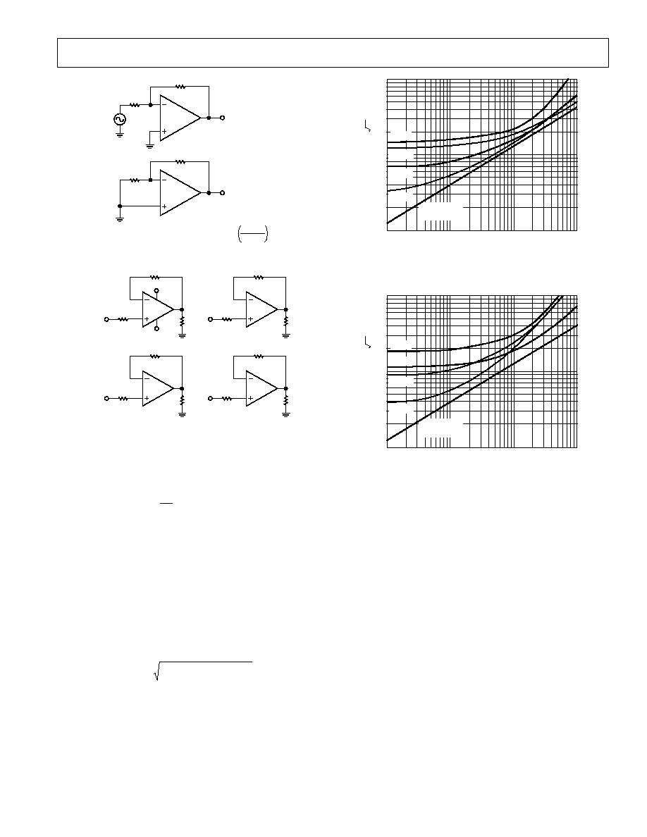
500
5k
V
1
20V p-p
1/4
OP471
50
50k
CHANNEL SEPARATION = 20 LOG
V
1
V
2
/ 1000
V
2
1/4
OP471
Figure 2. Channel Separation Test Circuit
7
6
5
1
2
3
+1V
+18V
4
≠18V
11
A
+1V
B
D
14
13
12
≠1V
C
8
9
10
≠1V
Figure 3. Burn-In Circuit
APPLICATIONS INFORMATION
Voltage and Current Noise
The OP471 is a very low-noise quad op amp, exhibiting a typical
voltage noise of only 6.5
Hz @ 1 kHz. The low noise character-
istic of the OP471 is, in part, achieved by operating the input
transistors at high collector currents since the voltage noise is
inversely proportional to the square root of the collector current.
Current noise, however, is directly proportional to the square
root of the collector current. As a result, the outstanding voltage
noise performance of the OP471 is gained at the expense of current
noise performance which is typical for low noise amplifiers.
To obtain the best noise performance in a circuit, it is vital to
understand the relationship between voltage noise (e
n
), current
noise (i
n
), and resistor noise (e
t
).
Total Noise and Source Resistance
The total noise of an op amp can be calculated by:
E
e
i R
e
n
n
n
S
t
=
( )
+
( )
+
( )
2
2
2
where:
E
n
= total input referred noise
e
n
= op amp voltage noise
i
n
= op amp current noise
e
t
= source resistance thermal noise
R
S
= source resistance
The total noise is referred to the input and at the output would
be amplified by the circuit gain.
RS ≠ SOURCE RESISTANCE ≠
100
1
100
100k
TOT
A
L
N
OISE ≠ nV/ Hz
10
10k
1k
OP11
OP400
OP471
OP470
RESISTOR
NOISE ONLY
Figure 4. Total Noise vs. Source Resistance (Including
Resistor Noise) at 1 kHz
RS ≠ SOURCE RESISTANCE ≠
100
1
100
100k
TOT
A
L
N
OISE ≠ nV/ Hz
10
10k
1k
OP11
OP400
OP471
OP470
RESISTOR
NOISE ONLY
Figure 5. Total Noise vs. Source Resistance (Including
Resistor Noise) at 10 Hz
Figure 4 shows the relationship between total noise at 1 kHz
and source resistance. For R
S
< 1 k
W the total noise is domi-
nated by the voltage noise of the OP471. As R
S
rises above 1 k
W,
total noise increases and is dominated by resistor noise rather
than by voltage or current noise of the OP471. When R
S
exceeds
20 k
W, current noise of the OP471 becomes the major contributor
to total noise.
Figure 5 also shows the relationship between total noise and source
resistance, but at 10 Hz. Total noise increases more quickly
than shown in Figure 4 because current noise is inversely pro-
portional to the square root of frequency. In Figure 5, current
noise of the OP471 dominates the total noise when R
S
> 5 k
W.
From Figures 4 and 5, it can be seen that to reduce total noise,
source resistance must be kept to a minimum. In applications
with a high source resistance, the OP400, with lower current
noise than the OP471, will provide lower total noise.
REV. A
OP471
≠8≠
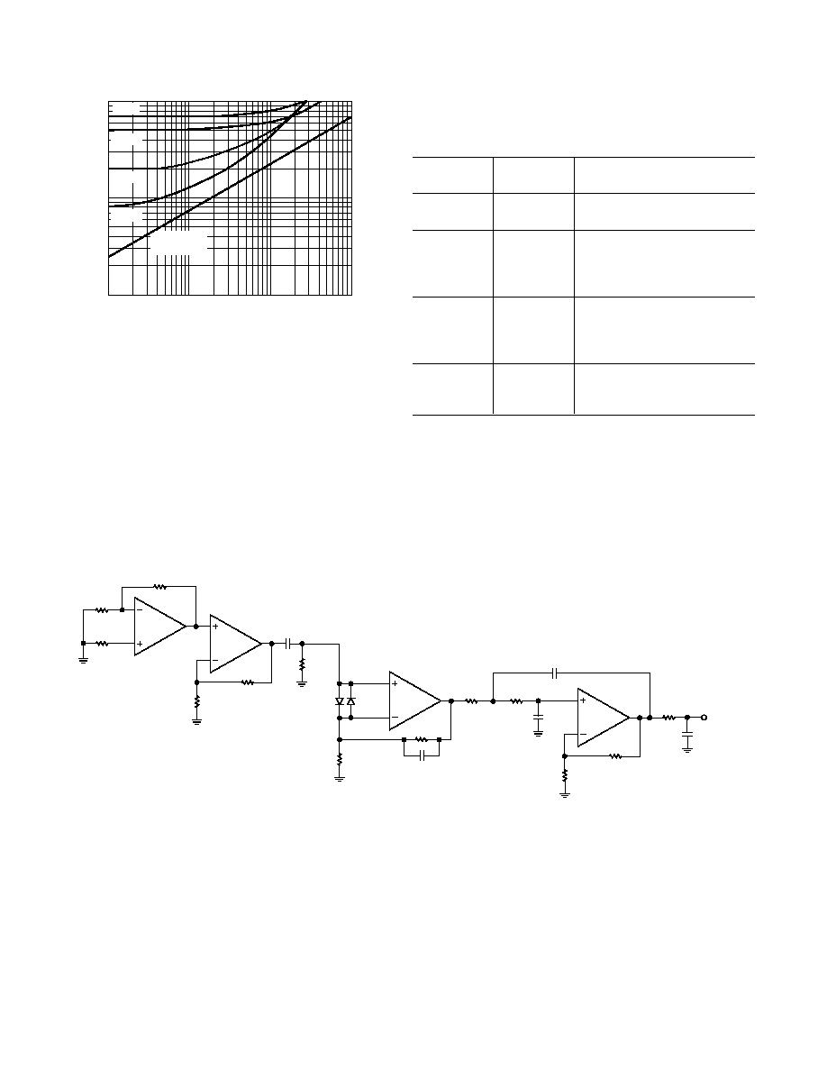
RS ≠ SOURCE RESISTANCE ≠
1000
10
100
100k
PEAK-T
O-PEAK NOISE ≠ nV
100
10k
1k
OP11
OP400
OP471
OP470
RESISTOR
NOISE ONLY
Figure 6. Peak-to-Peak Noise (0.1 Hz to 10 Hz) vs. Source
Resistance (Includes Resistor Noise)
Figure 6 shows peak-to-peak noise versus source resistance over
the 0.1 Hz to 10 Hz range. Once again, at low values of R
S
, the
voltage noise of the OP471 is the major contributor to peak-to-peak
noise. Current noise becomes the major contributor as R
S
increases.
The crossover point between the OP471 and the OP400 for
peak-to-peak noise is at R
S
= 17
W.
The OP470 is a lower noise version of the OP471, with a typical
noise voltage density of 3.2 nV/
˜Hz @ 1 kHz. The OP470 offers
lower offset voltage and higher gain than the OP471, but is a slower
speed device, with a slew rate of 2 V/
ms compared to a slew rate
of 8 V/
ms for the OP471.
R1
5
R3
1.24k
OP471
DUT
R2
5
R5
909
OP27E
R4
200
C1
2 F
R6
600k
R9
306k
OP15E
R8
10k
D1
1N4148
D2
1N4148
C2
0.032 F
R10
65.4k
R11
65.4k
C3
0.22 F
OP15E
C4
0.22 F
R13
5.9k
R12
10k
R14
4.99k
C5
1 F
e
OUT
GAIN = 50,000
V
S
= 15V
Figure 7. Peak-to-Peak Voltage Noise Test Circuit (0.1 Hz to 10 Hz)
For reference, typical source resistances of some signal sources
are listed in Table I.
TABLE I.
Source
Device
Impedance
Comments
Strain gauge
< 500
W
Typically used in
low-frequency applications.
Magnetic
< 1,500
W
Low I
B
very important to reduce
tapehead
self-magnetization problems
when direct coupling is used.
OP471 I
B
can be neglected.
Magnetic
< 1,500
W
Similar need for low I
B
in direct
phonograph
coupled applications. OP471
cartridges
will not introduce any
self -magnetization problem.
Linear variable
< 1,500
W
Used in rugged servo-feedback
differential
applications. Bandwidth of
transformer
interest is 400 Hz to 5 kHz.
*For further information regarding noise calculations, see "Minimization of
Noise in Op Amp Applications," Application Note AN-15.

REV. A
OP471
≠9≠
Noise Measurements - Peak-to-Peak Voltage Noise
The circuit of Figure 7 is a test setup for measuring peak-to-peak
voltage noise. To measure the 500 nV peak-to-peak noise speci-
fication of the OP471 in the 0.1 Hz to 10 Hz range, the following
precautions must be observed:
1. The device must be warmed up for at least five minutes. As
shown in the warm-up drift curve, the offset voltage typically
changes 13
mV due to increasing chip temperature after
power-up. In the 10-second measurement interval, these
temperature-induced effects can exceed tens-of-nanovolts.
2. For similar reasons, the device must be well-shielded from
air currents. Shielding also minimizes thermocouple effects.
3. Sudden motion in the vicinity of the device can also "feedthrough"
to increase the observed noise.
4. The test time to measure 0.1 Hz to 10 Hz noise should not exceed
10 seconds. As shown in the noise-tester frequency-response curve
of Figure 8, the 0.1 Hz corner is defined by only one pole. The
test time of 10 seconds acts as an additional pole to eliminate
noise contribution from the frequency band below 0.1 Hz.
5. A noise voltage density test is recommended when measuring
noise on a large number of units. A 10 Hz noise voltage density
measurement will correlate well with a 0.1 Hz to 10 Hz
peak-to-peak noise reading, since both results are determined
by the white noise and the location of the 1/f corner frequency.
6. Power should be supplied to the test circuit by well bypassed,
low noise supplies, e.g, batteries. These will minimize output
noise introduced through the amplifier supply pins.
FREQUENCY ≠ Hz
100
0.01
GAIN ≠ dB
80
60
40
20
0
0.1
1
10
100
Figure 8. 0.1 Hz to 10 Hz Peak-to-Peak Voltage Noise
Test Circuit Frequency Response
Noise Measurement - Noise Voltage Density
The circuit of Figure 9 shows a quick and reliable method of
measuring the noise voltage density of quad op amps. Each
individual amplifier is series connected and is in unity-gain, save
the final amplifier which is in a noninverting gain of 101. Since
the ac noise voltages of each amplifier are uncorrelated, they
add in rms fashion to yield:
e
= 101 e
+ e
e
e
OUT
nA
nB
nC
nD
2
2
2
2
+
+
À
^
Ø
The OP471 is a monolithic device with four identical amplifiers.
The noise voltage density of each individual amplifier will
match, giving:
e
101 4e
=
101
2e
OUT
n
n
2
=
À
^
Ø
( )
R2
10k
1/4
OP471
1/4
OP471
1/4
OP471
1/4
OP471
R1
100
e
OUT
TO SPECTRUM ANALYZER
e
OUT
(nV Hz) = 101(2e
n
)
V
S
= 15V
Figure 9. Noise Voltage Density Test Circuit
REV. A
OP471
≠10≠
Noise Measurement - Current Noise Density
The test circuit shown in Figure 10 can be used to measure current
noise density. The formula relating the voltage output to current
noise density is:
i
e
G
40nV / Hz
R
n
nOUT
S
=
À
¡
^
Ø
~ -
(
)
2
2
where:
G = gain of 10,000
R
S
= 100 k
W source resistance
Capacative Load Driving and Power Supply Considerations
The OP471 is unity-gain stable and is capable of driving large
capacitive loads without oscillating. Nonetheless, good supply
bypassing is highly recommended. Proper supply bypassing
reduces problems caused by supply line noise and improves the
capacitive load driving capability of the OP471.
R2
100k
R3
1.24k
OP471
DUT
R5
8.06k
OP27E
R4
200
e
n
OUT TO
SPECTRUM ANALYZER
R1
5
GAIN = 10,000
V
S
= 15V
Figure 10. Current Noise Density Test Circuit
R1
100 *
*
SEE TEXT
R3
50
OP471
C5
0.1 F
*
C4
10 F
+
V≠
V
OUT
C
L
1000pF
C1
200pF
R2
V
IN
PLACE SUPPLY DECOUPLING
CAPACITORS AT OP471
C3
0.1 F
C2
10 F
+
V+
Figure 11. Driving Large Capacitive Loads
In the standard feedback amplifier, the op amp's output resistance
combines with the load capacitance to form a lowpass filter that
adds phase shift in the feedback network and reduces stability. A
simple circuit to eliminate this effect is shown in Figure 11. The
added components, C1 and R3, decouple the amplifier from the
load capacitance and provide additional stability. The values of
C1 and R3 shown in Figure 11 are for load capacitances of up
to 1,000 pF when used with the OP471.
In applications where the OP471's inverting or noninverting inputs
are driven by a low source impedance (under 100
W) or connected
to ground, if V+ is applied before V≠, or when V≠ is disconnected,
excessive parasitic currents will flow.
Most applications use dual tracking supplies and with the device
supply pins properly bypassed, power-up will not present a
problem. A source resistance of at least 100
W in series with all
inputs (Figure 11) will limit the parasitic currents to a safe level
if V≠ is disconnected. It should be noted that any source resistance,
even 100
W, adds noise to the circuit. Where noise is required to
be kept at a minimum, a germanium or Schottky diode can be
used to clamp the V≠ pin and eliminate the parasitic current
flow instead of using series limiting resistors. For most applica-
tions, only one diode clamp is required per board or system.
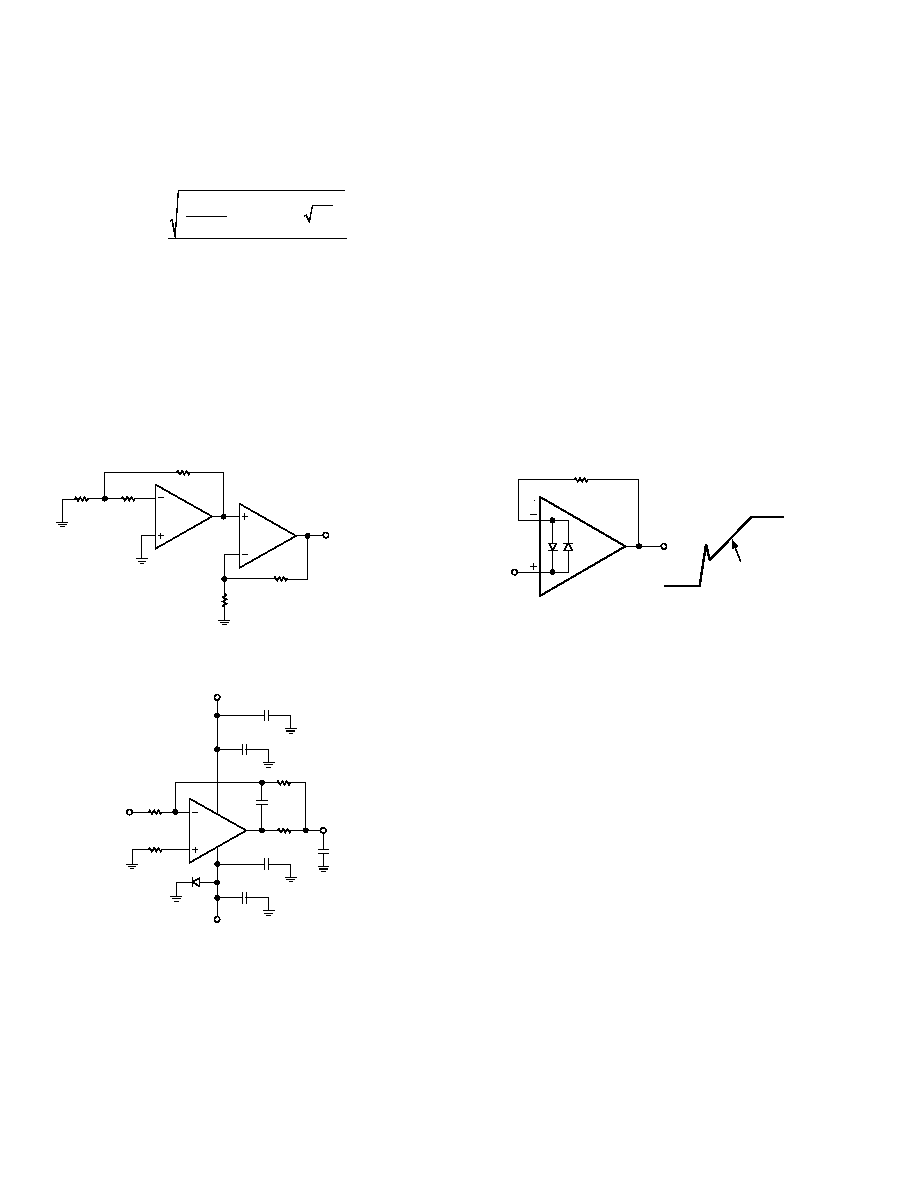
8V/ s
OP471
R
f
Figure 12. Pulsed Operation
Unity-Gain Buffer Applications
When R
f
£ 100 W and the input is driven with a fast, large signal
pulse (>1 V), the output waveform will look as shown in Figure 12.
During the fast feedthrough-like portion of the output, the input
protection diodes effectively short the output to the input, and a
current, limited only by the output short-circuit protection, will
be drawn by the signal generator. With R
f
500 W, the output
is capable of handling the current requirements (I
L
£ 20 mA at
10 V); the amplifier will stay in its active mode and a smooth
transition will occur.
When R
f
> 3 k
W, a pole created by R
f
and the amplifier's input
capacitance (2.6 pF) creates additional phase shift and reduces
phase margin. A small capacitor (20 pF to 50 pF) in parallel with
R
f
helps eliminate this problem.
APPLICATIONS
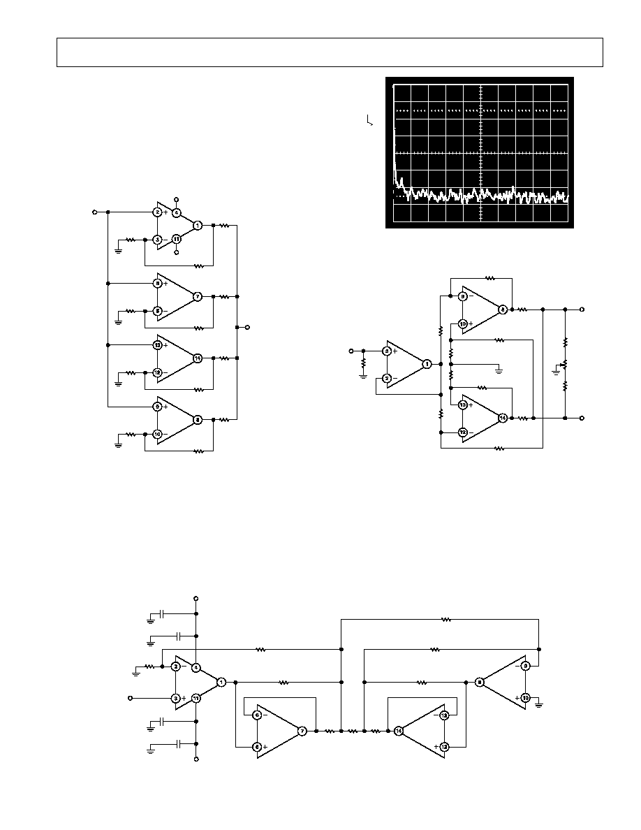
Low Noise Amplifier
A simple method of reducing amplifier noise by paralleling
amplifiers is shown in Figure 13. Amplifier noise, depicted in
Figure 14, is around 5 nV/
˜Hz @ 1 kHz (R.T.I.). Gain for each
paralleled amplifier and the entire circuit is 100. The 200
W
resistors limit circulating currents and provide an effective output
resistance of 50
W. The amplifier is stable with a 10 nF capacitive
load and can supply up to 30 mA of output drive.
REV. A
OP471
≠11≠
High-Speed Differential Line Driver
The circuit of Figure 15 is a unique line driver widely used in
professional audio applications. With
±18 V supplies, the line
driver can deliver a differential signal of 30 V p-p
into a 1.5 k
W
load. The output of the differential line driver looks exactly like
a transformer. Either output can be shorted to ground without
changing the circuit gain of 5, so the amplifier can easily be set
for inverting, noninverting, or differential operation. The line
driver can drive unbalanced loads, like a true transformer.
R2
5k
1/4
OP471E
+15V
≠15V
R3
200
R1
50
V
IN
R5
5k
1/4
OP471E
R6
200
R4
50
R8
5k
1/4
OP471E
R9
200
R7
50
R11
5k
1/4
OP471E
R12
200
R10
50
V
OUT
= 100V
IN
Figure 13. Low-Noise Amplifier
High-Output Amplifier
The amplifier shown in Figure 16 is capable of driving 20 V p-p
into a floating 400
W load. Design of the amplifier is based on a
bridge configuration. A1 amplifies the input signal and drives
the load with the help of A2. Amplifier A3 is a unity-gain inverter
which drives the load with help from A4. Gain of the high output
amplifier with the component values shown is 10, but can
easily be changed by varying R1 or R2.
NOISE DENSITY ≠ 0.58nV/ Hz/DIV
REFERRED
T
O
INPUT
10
0%
100
90
Figure 14. Noise Density of Low-Noise Amplifier, G = 100
R4
10k
1/4
OP471
R8
10k
R7
2k
R6
2k
R9
10k
1/4
OP471
R10
50
R2
2k
R3
2k
R5
10k
R14
1k
R12
1k
R13
10k
≠OUT
+OUT
1/4
OP471
R1
10k
IN
R11
50
Figure 15. High-Speed Differential Line Driver
1/4
OP471E
A1
R1
1k
V
IN
C3
0.1 F
C4
10 F
+
≠15V
C1
10 F
C2
0.1 F
+15V
R3
50
R2
9k
1/4
OP471E
A2
R4
50
R
L
R8
50
1/4
OP471E
A4
R7
50
R6
5k
R5
5k
1/4
OP471E
A3
+
Figure 16. High-Output Amplifier
REV. A
OP471
≠12≠
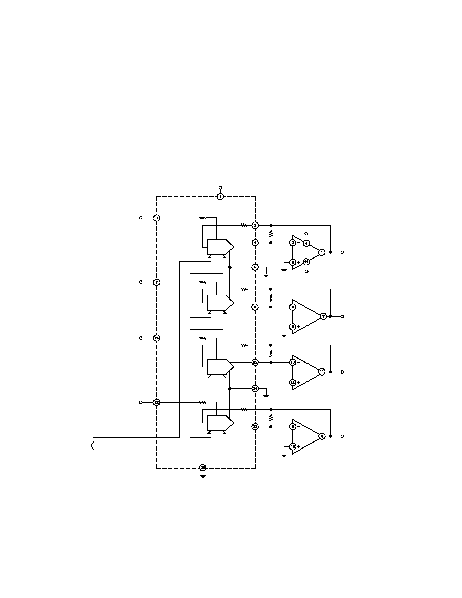
Quad Programmable Gain Amplifier
The combination of the quad OP471 and the DAC8408, a quad
8-bit CMOS DAC, creates a space-saving quad programmable gain
amplifier. The digital code present at the DAC, which is easily
set by a microprocessor, determines the ratio between the fixed
DAC feedback resistor and the impedance the DAC ladder presents
to the op amp feedback loop. Gain of each amplifier is:
V
V
= ≠
256
n
OUT
IN
where n equals the decimal equivalent of the 8-bit digital code
present at the DAC. If the digital code present at the DAC
consists of all zeros, the feedback loop will be open causing the
op amp output to saturate. The 20 M
W resistors placed in parallel
with the DAC feedback loop eliminates this problem with a very
small reduction in gain accuracy.
1/4
OP470E
+15V
≠15V
V
OUT
A
I
OUT1A
DAC A
V
REF
I
OUT2A/2B
R
FB
A
DGND
V
DD
DAC-8408ET
V
IN
A
DAC DATA BUS
PINS 9 (LSB) ≠ 16 (MSB)
R1
20M
1/4
OP470E
V
OUT
B
I
OUT1B
DAC B
V
REF
R
FB
B
V
IN
B
R2
20M
1/4
OP470E
V
OUT
C
I
OUT1C
DAC C
V
REF
R
FB
C
V
IN
C
R3
20M
1/4
OP470E
V
OUT
D
I
OUT1D
V
REF
R
FB
D
V
IN
D
R4
20M
DAC D
I
OUT2C/2D
A
B
C
D
Figure 17. Quad Programmable Gain Amplifier
REV. A
OP471
≠13≠
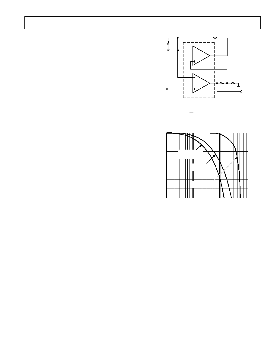
Low Phase Error Amplifier
The simple amplifier depicted in Figure 18 utilizes monolithic
matched operational amplifiers and a few resistors to substan-
tially reduce phase error compared to conventional amplifier
designs. At a given gain, the frequency range for a specified phase
accuracy is over a decade greater than for a standard single op
amp amplifier.
The low phase error amplifier performs second-order frequency
compensation through the response of op amp A2 in the feed-
back loop of A1. Both op amps must be extremely well matched
in frequency response. At low frequencies, the A1 feedback loop
forces V
2
/(K1 + 1) = V
IN
. The A2 feedback loop forces Vo/(K1 +1)
= V
2
/(K1 + 1) yielding an overall transfer function of V
O
/V
IN
=
K1 + 1. The dc gain is determined by the resistor divider at
the output, V
O
, and is not directly affected by the resistor divider
around A2. Note that similar to a conventional single op amp
amplifier, the dc gain is set by resistor ratios only. Minimum
gain for the low phase error amplifier is 10.
Figure 19 compares the phase error performance of the low
phase error amplifier with a conventional single op amp amplifier
and a cascaded two-stage amplifier. The low phase error amplifier
shows a much lower phase error, particularly for frequencies where
/
T
< 0.1. For example, phase error of ≠0.1
occurs at 0.002 /
T
for the single op amp amplifier, but at 0.11 /
T
for the low
phase error amplifier.
For more detailed information on the low phase error amplifier,
see Application Note AN-107.
R2
1/4
OP471E
A2
R1
V
O
= (K
1
+ 1) V
IN
1/4
OP471E
A1
R1
K1
V
O
R2
K1
V
IN
R2 = R1
ASSUME: A1 AND A2 ARE MATCHED.
A
O
(s) =
T
s
V2
Figure 18. Low Phase Error Amplifier
FREQUENCY RATIO ≠ 1/ , /
T
0
0.001
PHASE SHIFT ≠ Degrees
≠1
≠2
≠3
≠4
≠5
0.01
0.1
1
0.005
0.05
0.5
≠6
≠7
SINGLE OP AMP
(CONVENTIONAL
DESIGN)
CASCADED
(TWO STAGES)
LOW-PHASE ERROR
AMPLIFIER
Figure 19. Phase Error Comparison
REV. A
OP471
≠14≠
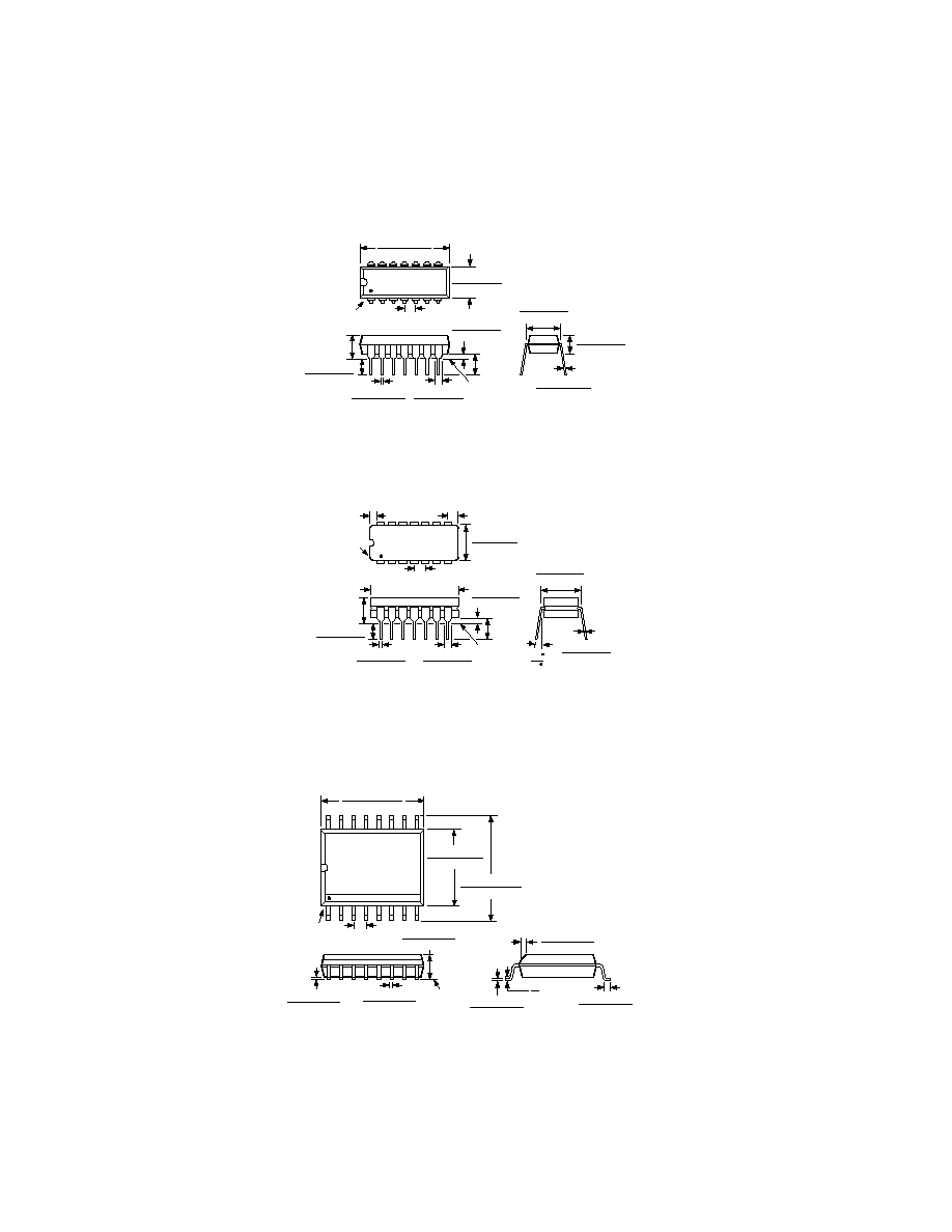
OUTLINE DIMENSIONS
Dimensions shown in inches and (mm).
14-Lead PDIP Package
(N-14)
14
1
7
8
PIN 1
0.795 (20.19)
0.725 (18.42)
0.280 (7.11)
0.240 (6.10)
0.100 (2.54)
BSC
SEATING
PLANE
0.060 (1.52)
0.015 (0.38)
0.210 (5.33)
MAX
0.022 (0.558)
0.014 (0.356)
0.160 (4.06)
0.115 (2.93)
0.070 (1.77)
0.045 (1.15)
0.130
(3.30)
MIN
0.195 (4.95)
0.115 (2.93)
0.015 (0.381)
0.008 (0.204)
0.325 (8.25)
0.300 (7.62)
14-Lead CERDIP Package
(Q-14)
14
1
7
8
0.310 (7.87)
0.220 (5.59)
PIN 1
0.005 (0.13) MIN 0.098 (2.49) MAX
0.100 (2.54) BSC
15
0
0.320 (8.13)
0.290 (7.37)
0.015 (0.38)
0.008 (0.20)
SEATING
PLANE
0.200 (5.08)
MAX
0.785 (19.94) MAX
0.150
(3.81)
MIN
0.200 (5.08)
0.125 (3.18)
0.023 (0.58)
0.014 (0.36)
0.070 (1.78)
0.030 (0.76)
0.060 (1.52)
0.015 (0.38)
16-Lead SOIC Package
(R-16)
SEATING
PLANE
0.0118 (0.30)
0.0040 (0.10)
0.0192 (0.49)
0.0138 (0.35)
0.1043 (2.65)
0.0926 (2.35)
0.050 (1.27)
BSC
16
9
8
1
0.4193 (10.65)
0.3937 (10.00)
0.2992 (7.60)
0.2914 (7.40)
PIN 1
0.4133 (10.50)
0.3977 (10.00)
0.0125 (0.32)
0.0091 (0.23)
8
0
0.0291 (0.74)
0.0098 (0.25)
45
0.0500 (1.27)
0.0157 (0.40)

REV. A
OP471
≠15≠
Revision History
Location
Page
Data Sheet changed from REV. 0 to REV. A.
Edits to FEATURES . . . . . . . . . . . . . . . . . . . . . . . . . . . . . . . . . . . . . . . . . . . . . . . . . . . . . . . . . . . . . . . . . . . . . . . . . . . . . . . . . . . . . 1
Edits to ELECTRICAL CHARACTERISTICS . . . . . . . . . . . . . . . . . . . . . . . . . . . . . . . . . . . . . . . . . . . . . . . . . . . . . . . . . . . . . . . . 2
Edits to ABSOLUTE MAXIMUM RATINGS . . . . . . . . . . . . . . . . . . . . . . . . . . . . . . . . . . . . . . . . . . . . . . . . . . . . . . . . . . . . . . . . . 3
Edits to ORDERING GUIDE . . . . . . . . . . . . . . . . . . . . . . . . . . . . . . . . . . . . . . . . . . . . . . . . . . . . . . . . . . . . . . . . . . . . . . . . . . . . . . 3
Deleted DICE CHARACTERISTICS . . . . . . . . . . . . . . . . . . . . . . . . . . . . . . . . . . . . . . . . . . . . . . . . . . . . . . . . . . . . . . . . . . . . . . . 5
Deleted WAFER TEST CHARACTERISTICS . . . . . . . . . . . . . . . . . . . . . . . . . . . . . . . . . . . . . . . . . . . . . . . . . . . . . . . . . . . . . . . . 5

≠16≠
C00307≠0≠4/02(A)
PRINTED IN U.S.A.