 | –≠–ª–µ–∫—Ç—Ä–æ–Ω–Ω—ã–π –∫–æ–º–ø–æ–Ω–µ–Ω—Ç: OP777ARM | –°–∫–∞—á–∞—Ç—å:  PDF PDF  ZIP ZIP |

REV. C
Information furnished by Analog Devices is believed to be accurate and
reliable. However, no responsibility is assumed by Analog Devices for its
use, nor for any infringements of patents or other rights of third parties that
may result from its use. No license is granted by implication or otherwise
under any patent or patent rights of Analog Devices.
a
OP777/OP727/OP747
One Technology Way, P.O. Box 9106, Norwood, MA 02062-9106, U.S.A.
Tel: 781/329-4700
www.analog.com
Fax: 781/326-8703
© Analog Devices, Inc., 2001
FEATURES
Low Offset Voltage: 100 V Max
Low Input Bias Current: 10 nA Max
Single-Supply Operation: 2.7 V to 30 V
Dual-Supply Operation: 1.35 V to 15 V
Low Supply Current: 300
A/Amp Max
Unity Gain Stable
No Phase Reversal
APPLICATIONS
Current Sensing (Shunt)
Line or Battery-Powered Instrumentation
Remote Sensors
Precision Filters
OP727 SOIC Pin-Compatible with LT1013
GENERAL DESCRIPTION
The OP777 , OP727 , and OP747 are precision single , dual,
and quad rail-to-rail output single- supply amplifiers featuring
micropower operation and rail-to-rail output ranges.
These
amplifier s provide improved performance over the industry
-standard
OP07 with
±15 V supplies , and offer the further advantage of true
single -supply operation down to 2.7 V , and smaller package
options than any other high-voltage precision bipolar amplifier.
Outputs are stable with capacitive loads of over 500 pF. Supply
current is less than 300
µA per amplifier at 5 V. 500 series resis-
tors protect the inputs, allowing input signal levels several volts above
the positive supply without phase reversal.
Applications for these amplifiers include both line-powered and
portable instrumentation, remote sensor signal conditioning, and
precision filters.
The OP777, OP727, and OP747 are specified over the extended
industrial (≠40
∞C to +85∞C) temperature range. The OP777,
single, is available in 8-lead MSOP and 8-lead SOIC packages.
The OP747, quad, is available in 14-lead TSSOP and narrow
14-lead SO packages. Surface-mount devices in TSSOP and MSOP
packages are available in tape and reel only.
The OP727, dual, is available in 8-lead TSSOP and 8-lead
SOIC packages. The OP727 8-lead SOIC pin configuration
differs from the standard 8-lead operational amplifier pinout.
FUNCTIONAL BLOCK DIAGRAMS
8-Lead MSOP
(RM-8)
IN
IN
V
V+
OUT
NC
NC
1
4
5
8
OP777
NC
NC = NO CONNECT
8-Lead SOIC
(R-8)
1
2
3
4
8
7
6
5
IN
V
+IN
V+
OUT
NC
NC
NC
NC = NO CONNECT
OP777
8-Lead TSSOP
(RU-8)
TOP VIEW
(Not to Scale)
8
7
6
5
1
2
3
4
OUT A
≠IN A
IN A
V≠
V
OUT B
≠IN B
IN B
OP727
14-Lead SOIC
(R-14)
TOP VIEW
(Not to Scale)
14
13
12
11
10
9
8
1
2
3
4
5
6
7
≠IN A
IN A
V
IN B
≠IN B
OUT B
OUT D
≠IN D
IN D
V≠
IN C
≠IN C
OUT C
OUT A
OP747
14-Lead TSSOP
(RU-14)
TOP VIEW
(Not to Scale)
14
13
12
11
10
9
8
1
2
3
4
5
6
7
≠IN A
IN A
V
IN B
≠IN B
OUT B
OUT D
≠IN D
IN D
V≠
IN C
≠IN C
OUT C
OUT A
OP747
Precision Micropower
Single-Supply Operational Amplifiers
8-Lead SOIC
(R-8)
TOP VIEW
(Not to Scale)
8
7
6
5
1
2
3
4
≠IN B
IN A
V≠
V
OUT B
≠IN A
OP727
IN B
OUT A
NOTE: THIS PIN CONFIGURATION DIFFERS
FROM THE STANDARD 8-LEAD
OPERATIONAL AMPLIFIER PINOUT.

REV. C
≠2≠
OP777/OP727/OP747≠SPECIFICATIONS
ELECTRICAL CHARACTERISTICS
Parameter
Symbol
Conditions
Min
Typ
Max
Unit
INPUT CHARACTERISTICS
Offset Voltage OP777
V
OS
+25 C < T
A
< +85 C
20
100
µV
≠40
∞C < T
A
< +85
∞C
50
200
µV
Offset Voltage OP727/OP747
+25 C < T
A
< +85 C
30
160
µV
≠40
∞C < T
A
< +85
∞C
60
300
µV
Input Bias Current
I
B
≠40
∞C < T
A
< +85
∞C
5.5
11
nA
Input Offset Current
I
OS
≠40
∞C < T
A
< +85
∞C
0.1
2
nA
Input Voltage Range
0
4
V
Common-Mode Rejection Ratio
CMRR
V
CM
= 0 V to 4 V
104
110
dB
Large Signal Voltage Gain
A
VO
R
L
= 10 k
, V
O
= 0.5 V to 4.5 V
300
500
V/mV
Offset Voltage Drift OP777
V
OS
/
T
≠40
∞C < T
A
< +85
∞C
0.3
1.3
µV/∞C
Offset Voltage Drift OP727/OP747
V
OS
/
T
≠40
∞C < T
A
< +85
∞C
0.4
1.5
µV/∞C
OUTPUT CHARACTERISTICS
Output Voltage High
V
OH
I
L
= 1 mA, ≠40
∞C to +85 ∞C
4.88
4.91
V
Output Voltage Low
V
OL
I
L
= 1 mA, ≠40
∞C to +85 ∞C
126
140
mV
Output Circuit
I
OUT
V
DROPOUT
< 1 V
±10
mA
POWER SUPPLY
Power Supply Rejection Ratio
PSRR
V
S
= 3 V to 30 V
120
130
dB
Supply Current/Amplifier OP777
I
SY
V
O
= 0 V
220
270
µA
≠40
∞C < T
A
< +85
∞C
270
320
µA
Supply Current/Amplifier OP727/OP747
V
O
= 0 V
235
290
µA
≠40
∞C < T
A
< +85
∞C
290
350
µA
DYNAMIC PERFORMANCE
Slew Rate
SR
R
L
= 2 k
0.2
V/
µs
Gain Bandwidth Product
GBP
0.7
MHz
NOISE PERFORMANCE
Voltage Noise
e
n
p-p
0.1 Hz to 10 Hz
0.4
µV p-p
Voltage Noise Density
e
n
f = 1 kHz
15
nV/
Hz
Current Noise Density
i
n
f = 1 kHz
0.13
pA/
Hz
NOTES
Typical specifications: >50% of units perform equal to or better than the "typical" value.
Specifications subject to change without notice.
(@ V
S
= 5.0 V, V
CM
= 2.5 V, T
A
= 25 C unless otherwise noted.)

REV. C
≠3≠
OP777/OP727/OP747
ELECTRICAL CHARACTERISTICS
Parameter
Symbol
Conditions
Min
Typ
Max
Unit
INPUT CHARACTERISTICS
Offset Voltage OP777
V
OS
+25
∞C < T
A
< +85
∞C
30
100
µV
≠40
∞C < T
A
< +85
∞C
50
200
µV
Offset Voltage OP727/OP747
V
OS
+25
∞C < T
A
< +85
∞C
30
160
µV
≠40
∞C < T
A
< +85
∞C
50
300
µV
Input Bias Current
I
B
≠40
∞C < T
A
< +85
∞C
5
10
nA
Input Offset Current
I
OS
≠40
∞C < T
A
< +85
∞C
0.1
2
nA
Input Voltage Range
≠15
+14
V
Common-Mode Rejection Ratio
CMRR
V
CM
= ≠15 V to +14 V
110
120
dB
Large Signal Voltage Gain
A
VO
R
L
= 10 k
, V
O
= ≠14.5 V to +14.5 V
1,000
2,500
V/mV
Offset Voltage Drift OP777
V
OS
/
T ≠40∞C < T
A
< +85
∞C
0.3
1.3
µV/∞C
Offset Voltage Drift OP727/OP747
V
OS
/
T ≠40∞C < T
A
< +85
∞C
0.4
1.5
µV/∞C
OUTPUT CHARACTERISTICS
Output Voltage High
V
OH
I
L
= 1 mA, ≠40
∞C to +85 ∞C
+14.9
+14.94
V
Output Voltage Low
V
OL
I
L
= 1 mA, ≠40
∞C to +85 ∞C
≠14.94
≠14.9
V
Output Circuit
I
OUT
±30
mA
POWER SUPPLY
Power Supply Rejection Ratio
PSRR
V
S
=
± 1.5 V to ± 15 V
120
130
dB
Supply Current/Amplifier OP777
I
SY
V
O
= 0 V
300
350
µA
≠40
∞C < T
A
< +85
∞C
350
400
µA
Supply Current/Amplifier OP727/747
V
O
= 0 V
320
375
µA
≠40
∞C < T
A
< +85
∞C
375
450
µA
DYNAMIC PERFORMANCE
Slew Rate
SR
R
L
= 2 k
0.2
V/
µs
Gain Bandwidth Product
GBP
0.7
MHz
NOISE PERFORMANCE
Voltage Noise
e
n
p-p
0.1 Hz to 10 Hz
0.4
µV p-p
Voltage Noise Density
e
n
f = 1 kHz
15
nV/
Hz
Current Noise Density
i
n
f = 1 kHz
0.13
pA/
Hz
Specifications subject to change without notice.
(@ 15 V, V
CM
= 0 V, T
A
= 25 C unless otherwise noted.)

REV. C
OP777/OP727/OP747
≠4≠
ABSOLUTE MAXIMUM RATINGS
1, 2
Supply Voltage . . . . . . . . . . . . . . . . . . . . . . . . . . . . . . . . . 36 V
Input Voltage . . . . . . . . . . . . . . . . . . . . ≠V
S
≠ 5 V to +V
S
+ 5 V
Differential Input Voltage . . . . . . . . . . . . . .
± Supply Voltage
Output Short-Circuit Duration to GND . . . . . . . . . Indefinite
Storage Temperature Range
RM, R, RU Packages . . . . . . . . . . . . . . . . ≠65
∞C to +150∞C
Operating Temperature Range
OP777/OP727/OP747 . . . . . . . . . . . . . . . ≠40
∞C to +85∞C
Junction Temperature Range
RM, R, RU Packages . . . . . . . . . . . . . . . . ≠65
∞C to +150∞C
Lead Temperature Range (Soldering, 60 sec) . . . . . . . 300
∞C
Electrostatic Discharge (Human Body Model) . . . . 2000 V max
Package Type
JA
3
JC
Unit
8-Lead MSOP (RM)
190
44
∞C/W
8-Lead SOIC (R)
158
43
∞C/W
8-Lead TSSOP (RU)
240
43
∞C/W
14-Lead SOIC (R)
120
36
∞C/W
14-Lead TSSOP (RU)
180
35
∞C/W
NOTES
1
Absolute maximum ratings apply at 25
∞C, unless otherwise noted.
2
Stresses above those listed under Absolute Maximum Ratings may cause perma-
nent damage to the device. This is a stress rating only; functional operation of the
device at these or any other conditions above those listed in the operational
sections of this specification is not implied. Exposure to absolute maximum rating
conditions for extended periods may affect device reliability.
3
JA
is specified for worst-case conditions, i.e.,
JA
is specified for device soldered in
circuit board for surface-mount packages.
ORDERING GUIDE
Temperature
Package
Package
Branding
Model
Range
Description
Option
Information
OP777ARM
≠40
∞C to +85 ∞C
8-Lead MSOP
RM-8
A1A
OP777AR
≠40
∞C to +85 ∞C
8-Lead SOIC
SO-8
OP727ARU
≠40
∞C to +85 ∞C
8-Lead TSSOP
RU-8
OP727AR
≠40
∞C to +85 ∞C
8-Lead SOIC
SO-8
OP747AR
≠40
∞C to +85 ∞C
14-Lead SOIC
R-14
OP747ARU
≠40
∞C to +85 ∞C
14-Lead TSSOP
RU-14
CAUTION
ESD (electrostatic discharge) sensitive device. Electrostatic charges as high as 4000 V readily
accumulate on the human body and test equipment and can discharge without detection. Although
the OP777/OP727/OP747 features proprietary ESD protection circuitry, permanent damage may
occur on devices subjected to high-energy electrostatic discharges. Therefore, proper ESD
precautions are recommended to avoid performance degradation or loss of functionality.
WARNING!
ESD SENSITIVE DEVICE

REV. C
≠5≠
OP777/OP727/OP747
Typical Performance Characteristics≠
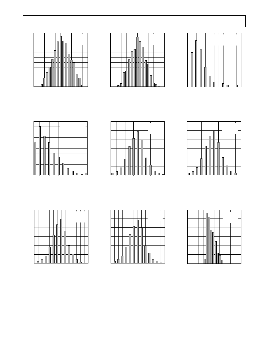
OFFSET VOLTAGE ≠ V
220
60
0
100
80 60
40 20
0
20
40
60 80 100
200
80
40
20
160
120
140
100
180
V
SY
= 15V
V
CM
= 0V
T
A
= 25 C
NUMBER OF AMPLIFIERS
TPC 1. OP777 Input Offset Voltage
Distribution
TCV
OS
≠ V/ C
QUANTITY
≠
Amplifiers
200
100
0
1.0
0.2
0.4
0.6
0.8
180
140
60
40
V
SY
= 15V
V
CM
= 0V
T
A
= ≠40 C TO +85 C
80
160
120
20
0.1
0.3
0.5
0.7
0.9
1.1 1.2
TPC 4. OP727/OP747 Input Offset
Voltage Drift (TCV
OS
Distribution)
OFFSET VOLTAGE ≠ V
300
0
120
80
0
40
80
400
200
100
600
NUMBER OF AMPLIFIERS
40
120
140
V
SY
= 5V
V
CM
= 2.5V
T
A
= 25 C
500
TPC 7. OP727 Input Offset Voltage
Distribution
OFFSET VOLTAGE ≠ V
220
60
0
100
80 60
40 20
0
20
40
60 80 100
200
80
40
20
160
120
140
100
180
V
SY
= 5V
V
CM
= 2.5V
T
A
= 25 C
NUMBER OF AMPLIFIERS
TPC 2. OP777 Input Offset Voltage
Distribution
V
QUANTITY
≠
Amplifiers
600
400
0
300
200
V
SY
= 15V
V
CM
= 0V
T
A
= 25 C
500
100
≠120
≠80
≠40
0
40
80
120
TPC 5. OP747 Input Offset Voltage
Distribution
120
140
OFFSET VOLTAGE ≠ V
300
0
80
0
40
80
40
120
400
200
100
500
600
V
SY
= 15V
V
CM
= 0V
T
A
= 25 C
NUMBER OF AMPLIFIERS
TPC 8. OP727 Input Offset Voltage
Distribution
INPUT OFFSET DRIFT ≠ V/ C
NUMBER OF AMPLIFIERS
30
15
0
0
1.2
0.2
0.4
0.6
0.8
1.0
25
20
10
5
V
SY
= 15V
V
CM
= 0V
T
A
= 40 C TO +85 C
TPC 3. OP777 Input Offset Voltage
Drift Distribution
OFFSET VOLTAGE ≠ V
NUMBER OF AMPLIFIERS
600
300
0
500
400
200
100
V
SY
= 5V
V
CM
= 2.5V
T
A
= 25 C
≠120
≠80
≠40
0
40
80
120
TPC 6. OP747 Input Offset Voltage
Distribution
INPUT BIAS CURRENT ≠ nA
NUMBER OF AMPLIFIERS
30
15
0
3
8
4
5
6
7
25
20
10
5
V
SY
= 15V
V
CM
= 0V
T
A
= 25 C
TPC 9. Input Bias Current
Distribution

REV. C
OP777/OP727/OP747
≠6≠
LOAD CURRENT ≠ mA
OUTPUT VOLTAGE
≠
mV
10k
100
0
0.001
0.01
100
0.1
1
10
1.0
V
S
= 15V
T
A
= 25 C
0.1
10
1k
SINK
SOURCE
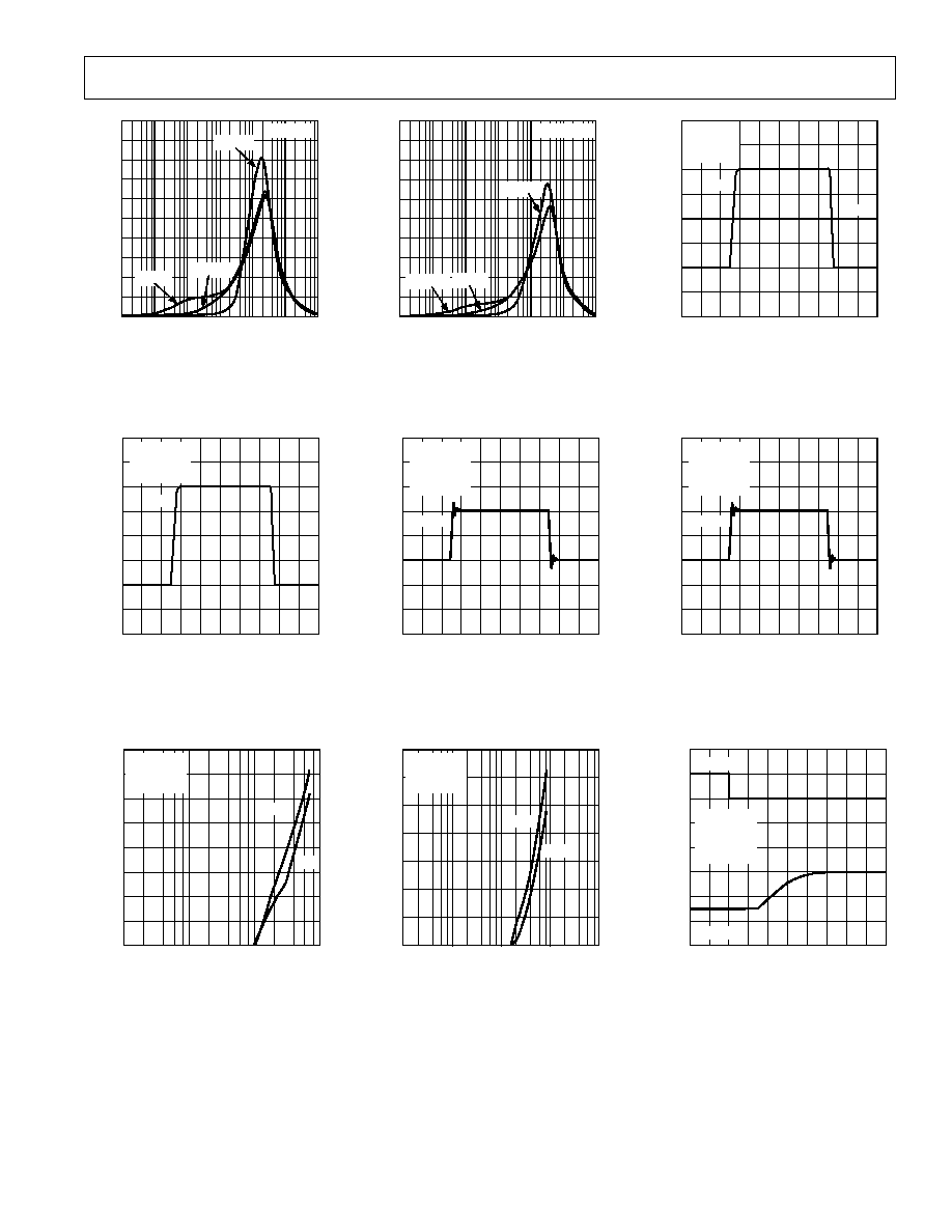
TPC 10. Output Voltage to Supply
Rail vs. Load Current
TEMPERATURE ≠ C
SUPPLY CURRENT
≠
A
500
500
60
40
140
20 0
20
40
60
80 100 120
200
100
200
400
100
300
I
SY+
(V
SY
= 15V)
I
SY+
(V
SY
= 5V)
0
400
I
SY
(V
SY
= 5V)
I
SY
(V
SY
= 15V)
300
TPC 13. Supply Current vs.
Temperature
FREQUENCY ≠ Hz
100
100k
100M
1k
10k
1M
10M
V
SY
= 5V
C
LOAD
= 0
R
LOAD
=
PHASE SHIFT
≠
Degrees
45
90
135
180
225
270
0
OPEN-LOOP GAIN
≠
dB
120
100
80
40
20
0
≠20
≠40
≠60
140
60
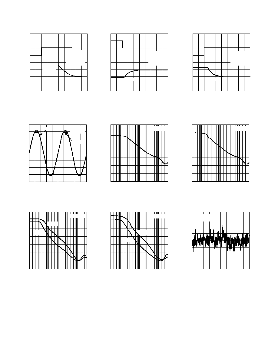
TPC 16. Open Loop Gain and
Phase Shift vs. Frequency
LOAD CURRENT ≠ mA
OUTPUT VOLTAGE
≠
mV
10k
100
0
0.001
0.01
100
0.1
1
10
1.0
SOURCE
V
S
= 5V
T
A
= 25 C
0.1
10
1k
SINK
TPC 11. Output Voltage to Supply
Rail vs. Load Current
SUPPLY VOLTAGE ≠ V
SUPPLY CURRENT
≠
A
350
0
0
5
35
10
15
20
25
30
300
200
150
100
50
250
T
A
= 25 C
TPC 14. Supply Current vs. Supply
Voltage
CLOSED-LOOP GAIN
≠
dB
60
50
40
40
30
20
10
0
10
20
30
FREQUENCY ≠ Hz
1k
10k
100M
100k
1M
10M
V
SY
= 15V
C
LOAD
= 0
R
LOAD
= 2k
A
V
= 100
A
V
= 10
A
V
= +1
TPC 17. Closed Loop Gain vs.
Frequency
TEMPERATURE ≠ C
INPUT BIAS CURRENT
≠
nA
6
4
0
60
40
140
20 0
20
40
60
80 100 120
5
1
3
2
V
SY
= 15V
TPC 12. Input Bias Current vs.
Temperature
FREQUENCY ≠ Hz
OPEN-LOOP GAIN
≠
dB
120
100
80
40
20
0
≠20
≠40
≠60
140
60
10
100k
100M
100
1k
10k
1M
10M
PHASE SHIFT
≠
De
g
rees
45
90
135
180
225
270
0
V
SY
= 15V
C
LOAD
= 0
R
LOAD
=
TPC 15. Open Loop Gain and
Phase Shift vs. Frequency
FREQUENCY ≠ Hz
1k
10k
100M
100k
1M
10M
V
SY
= 5V
C
LOAD
= 0
R
LOAD
= 2k
A
V
= 100
A
V
= 10
A
V
= +1
CLOSED-LOOP GAIN
≠
dB
60
50
40
40
30
20
10
0
10
20
30
TPC 18. Closed Loop Gain vs.
Frequency

REV. C
≠7≠
OP777/OP727/OP747
FREQUENCY ≠ Hz
OUTPUT IMPEDANCE
≠
300
270
0
240
210
180
150
120
90
60
30
100
100k
100M
1k
10k
1M
10M
V
SY
= 5V
A
V
= 1
A
V
= 10
A
V
= 100
TPC 19. Output Impedance vs.
Frequency
TIME ≠ 100 s/DIV
VOLTAGE
≠
1V/DIV
V
SY
= 15V
R
L
= 2k
C
L
= 300pF
A
V
= 1
0V
TPC 22. Large Signal Transient
Response
CAPACITANCE ≠ pF
SMALL SIGNAL OVERSHOOT
≠
%
40
35
0
1
10
1k
100
30
25
5
20
15
10
V
SY
= 2.5V
R
L
= 2k
V
IN
= 100mV
OS
OS
TPC 25. Small Signal Overshoot
vs. Load Capacitance
FREQUENCY ≠ Hz
100
100k
100M
1k
10k
1M
10M
V
SY
= 15V
A
V
= 1
A
V
= 10
A
V
= 100
OUTPUT IMPEDANCE
≠
300
270
0
240
210
180
150
120
90
60
30
TPC 20. Output Impedance vs.
Frequency
TIME ≠ 10 s/DIV
VOLTAGE
≠
50mV/DIV
V
SY
= 2.5V
C
L
= 300pF
R
L
= 2k
V
IN
= 100mV
A
V
= 1
TPC 23. Small Signal Transient
Response
CAPACITANCE ≠ pF
SMALL SIGNAL OVERSHOOT
≠
%
35
0
1
10
10k
100
30
25
5
20
15
10
V
SY
= 15V
R
L
= 2k
V
IN
= 100mV
1k
+OS
OS
TPC 26. Small Signal Overshoot
vs. Load Capacitance
TIME ≠ 100 s/DIV
VOLTAGE
≠
1V/DIV
V
SY
= 2.5V
R
L
= 2k
C
L
= 300pF
A
V
= 1
0V
TPC 21. Large Signal Transient
Response
TIME ≠ 10 s/DIV
VOLTAGE
≠
50mV/DIV
V
SY
= 15V
C
L
= 300pF
R
L
= 2k
V
IN
= 100mV
A
V
= 1
TPC 24. Small Signal Transient
Response
TIME ≠ 40 s/DIV
INPUT
OUTPUT
V
SY
= 15V
R
L
= 10k
A
V
= 100
V
IN
= 200mV
+200mV
0V
0V
10V
TPC 27. Negative Overvoltage
Recovery

REV. C
OP777/OP727/OP747
≠8≠
TIME ≠ 40 s/DIV
INPUT
OUTPUT
V
SY
= 15V
R
L
= 10k
A
V
= 100
V
IN
= 200mV
200mV
0V
0V
10V
TPC 28. Positive Overvoltage
Recovery
TIME ≠ 400 s/DIV
VOLTAGE
≠
5V/DIV
INPUT
OUTPUT
V
S
= 15V
A
V
= 1
TPC 31. No Phase Reversal
FREQUENCY ≠ Hz
PSRR
≠
dB
0
10
10k
10M
140
120
100
80
60
40
20
100
1k
100k
1M
+PSRR
PSRR
V
SY
= 2.5V
TPC 34. PSRR vs. Frequency
TIME ≠ 40 s/DIV
INPUT
OUTPUT
200mV
0V
V
SY
= 2.5V
R
L
= 10k
A
V
= 100
V
IN
= 200mV
2V
0V
TPC 29. Negative Overvoltage
Recovery
FREQUENCY ≠ Hz
CMRR
≠
dB
0
10
10k
10M
140
120
100
80
60
40
20
100
1k
100k
1M
V
SY
= 2.5V
TPC 32. CMRR vs. Frequency
FREQUENCY ≠ Hz
PSRR
≠
dB
0
10
10k
10M
140
120
100
80
60
40
20
100
1k
100k
1M
V
SY
= 15V
+PSRR
PSRR
TPC 35. PSRR vs. Frequency
TIME ≠ 40 s/DIV
INPUT
OUTPUT
0V
0V
2V
V
SY
= 2.5V
R
L
= 10k
A
V
= 100
V
IN
= 200mV
200mV
TPC 30. Positive Overvoltage
Recovery
FREQUENCY ≠ Hz
CMRR
≠
dB
0
10
10k
10M
140
120
100
80
60
40
20
100
1k
100k
1M
V
SY
= 15V
TPC 33. CMRR vs. Frequency
TIME ≠ 1s/DIV
VOLTAGE
≠
1V/DIV
V
SY
= 5V
GAIN = 10M
TPC 36. 0.1 Hz to 10 Hz Input
Voltage Noise

REV. C
≠9≠
OP777/OP727/OP747
TIME ≠ 1s/DIV
V
SY
= 15V
GAIN = 10M
VOLTAGE
≠
1V/DIV
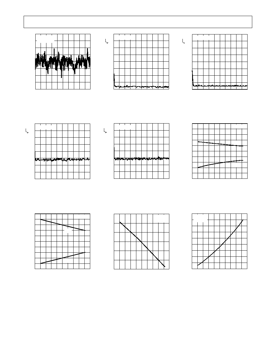
TPC 37. 0.1 Hz to 10 Hz Input
Voltage Noise
V
SY
= 15V
VOLTAGE NOISE DENSITY
≠
nV/ Hz
FREQUENCY ≠ Hz
0
0
2.5k
500
1k
1.5k
2.0k
5
10
15
20
25
30
35
40
TPC 40. Voltage Noise Density
TEMPERATURE ≠ C
SHORT CIRCUIT CURRENT
≠
mA
50
50
60
40
140
20 0
20
40
60
80 100 120
40
30
10
40
20
V
SY
= 15V
20
10
0
30
I
SC
I
SC+
TPC 43. Short Circuit Current vs.
Temperature
VOLTAGE NOISE DENSITY
≠
nV/ Hz
FREQUENCY ≠ Hz
10
0
500
100
200
300
400
20
30
40
50
60
70
80
90
V
SY
= 15V
TPC 38. Voltage Noise Density
V
SY
= 2.5V
VOLTAGE NOISE DENSITY
≠
nV/ Hz
FREQUENCY ≠ Hz
0
0
2.5k
500
1k
1.5k
2.0k
5
10
15
20
25
30
35
40
TPC 41. Voltage Noise Density
TEMPERATURE ≠ C
OUTPUT VOLTAGE HIGH
≠
V
4.95
4.92
4.89
60
40
140
20
0
20 40
60
80 100 120
4.94
4.93
4.91
4.90
V
SY
= 5V
I
L
= 1mA
TPC 44. Output Voltage High vs.
Temperature
V
SY
= 2.5V
VOLTAGE NOISE DENSITY
≠
nV/ Hz
FREQUENCY ≠ Hz
10
0
500
100
200
300
400
20
30
40
50
60
70
80
90
TPC 39. Voltage Noise Density
TEMPERATURE ≠ C
SHORT CIRCUIT CURRENT
≠
mA
50
50
60
40
140
20 0
20
40
60
80 100 120
40
30
10
40
20
V
SY
= 5V
20
10
0
30
I
SC
I
SC+
TPC 42. Short Circuit Current vs.
Temperature
TEMPERATURE ≠ C
OUTPUT VOLTAGE LOW
≠
mV
70
60
40
140
20
0
20 40
60
80 100 120
80
90
100
110
120
130
140
150
160
V
SY
= 5V
I
L
= 1mA
TPC 45. Output Voltage Low vs.
Temperature

REV. C
OP777/OP727/OP747
≠10≠
TEMPERATURE ≠ C
OUTPUT VOLTAGE HIGH
≠
V
14.944
60
40
140
20 0
20 40
60
80 100 120
14.946
14.948
14.950
14.954
14.956
14.958
14.960
14.962
14.964
V
SY
= 15V
I
L
= 1mA
14.952
TPC 46. Output Voltage High vs.
Temperature
TEMPERATURE ≠ C
OUTPUT VOLTAGE LOW
≠
V
14.960
60
40
140
V
SY
= 15V
I
L
= 1mA
20
0
20 40
60
80 100 120
14.955
14.950
14.945
14.935
14.930
14.940
TPC 47. Output Voltage Low vs.
Temperature
TIME ≠ Minutes
V
OS
≠
V
1.5
0
1.5
0
0.5
5.0
1.0 1.5 2.0 2.5 3.0 3.5 4.0 4.5
1.0
0.5
0.5
1.0
V
SY
= 15V
V
CM
= 0V
T
A
= 25 C
TPC 48. Warm-Up Drift
BASIC OPERATION
The OP777/OP727/OP747 amplifier uses a precision Bipolar
PNP input stage coupled with a high-voltage CMOS output
stage. This enables this amplifier to feature an input voltage
range which includes the negative supply voltage (often ground-
in single-supply applications) and also swing to within 1 mV of the
output rails. Additionally, the input voltage range extends to within
1 V of the positive supply rail. The epitaxial PNP input structure
provides high breakdown voltage, high gain, and an input bias cur-
rent figure comparable to that obtained with a "Darlington" input
stage amplifier but without the drawbacks (i.e., severe penalties for
input voltage range, offset, drift and noise). The PNP input structure
also greatly lowers the noise and reduces the dc input error terms.
Supply Voltage
The amplifiers are fully specified with a single 5 V supply and, due
to design and process innovations, can also operate with a supply
voltage from 2.7 V up to 30 V. This allows operation from most
split supplies used in current industry practice, with the advantage
of substantially increased input and output voltage ranges over
conventional split-supply amplifiers. The OP777/OP727/OP747
series is specified with (V
SY
= 5 V, V≠ = 0 V and V
CM
= 2.5 V
which is most suitable for single-supply application. With PSRR of
130 dB (0.3
µV/V) and CMRR of 110 dB (3 µV/V) offset is mini-
mally affected by power supply or common-mode voltages. Dual
supply,
±15 V operation is also fully specified.
Input Common-Mode Voltage Range
The OP777/OP727/OP747 is rated with an input common-mode
voltage which extends from the minus supply to within 1 V of the
positive supply. However, the amplifier can still operate with input
voltages slightly below V
EE
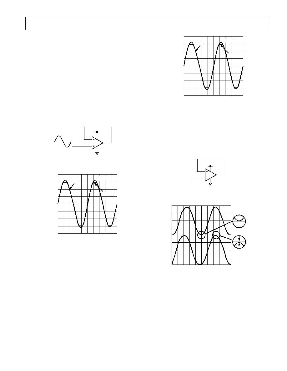
. In Figure 2, OP777/OP727/OP747 is
configured as a difference amplifier with a single supply of 2.7 V
and negative dc common-mode voltages applied at the inputs
terminals. A 400 mV p-p input is then applied to the noninverting
input. It can be seen from the graph below that the output does not
show any distortion. Micropower operation is maintained by using
large input and feedback resistors.
TIME ≠ 0.2ms/DIV
VOLTAGE
≠
100
V/DIV
V
IN
V
OUT
0V
Figure 1. Input and Output Signals with V
CM
< 0 V
+3V
OP777/
OP727/
OP747
100k
100k
100k
100k
0.1V
V
IN
= 1kHz at 400mV p-p
0.27V
Figure 2. OP777/OP727/OP747 Configured as a Differ-
ence Amplifier Operating at V
CM
< 0 V

REV. C
OP777/OP727/OP747
≠11≠
Input Over Voltage Protection
When the input of an amplifier is more than a diode drop below
V
EE
, or above V
CC
, large currents will flow from the substrate
(V≠) or the positive supply (V+), respectively, to the input pins
which can destroy the device. In the case of OP777/OP727/
OP747, differential voltages equal to the supply voltage will not
cause any problem (see Figure 3). OP777/OP727/OP747 has
built- in 500
internal current limiting resistors, in series with the
inputs, to minimize the chances of damage. It is a good practice to
keep the current flowing into the inputs below 5 mA. In this con-
text it should also be noted that the high breakdown of the input
transistors removes the necessity for clamp diodes between the
inputs of the amplifier, a feature that is mandatory on many preci-
sion op amps. Unfortunately, such clamp diodes greatly interfere
with many application circuits such as precision rectifiers and
comparators. The OP777/OP727/OP747 series is free from such
limitations.
30V
V p-p = 32V
OP777/
OP727/
OP747
Figure 3a. Unity Gain Follower
TIME ≠ 400 s/DIV
VOLTAGE
≠
5V/DIV
V
SY
= 15V
V
IN
V
OUT
Figure 3b. Input Voltage Can Exceed the Supply Voltage
Without Damage
Phase Reversal
Many amplifiers misbehave when one or both of the inputs are
forced beyond the input common-mode voltage range. Phase
reversal is typified by the transfer function of the amplifier effectively
reversing its transfer polarity. In some cases this can cause lockup in
servo systems and may cause permanent damage or nonrecoverable
parameter shifts to the amplifier. Many amplifiers feature compensa-
tion circuitry to combat these effects, but some are only effective for
the inverting input. Additionally, many of these schemes only work
for a few hundred millivolts or so beyond the supply rails. OP777/
OP727/OP747 has a protection circuit against phase reversal
when one or both inputs are forced beyond their input common-
mode voltage range. It is not recommended that the parts be
continuously driven more than 3 V beyond the rails.
TIME ≠ 400 s/DIV
VOLTAGE
≠
5V/DIV
V
SY
= 15V
V
IN
V
OUT
Figure 4. No Phase Reversal
Output Stage
The CMOS output stage has excellent (and fairly symmetric) output
drive and with light loads can actually swing to within 1 mV of both
supply rails. This is considerably better than similar amplifiers
featuring (so-called) rail-to-rail bipolar output stages. OP777/
OP727/OP747 is stable in the voltage follower configuration and
responds to signals as low as 1 mV above ground in single supply
operation.
2.7V TO 30V
V
IN
= 1mV
OP777/
OP727/
OP747
V
OUT
= 1mV
Figure 5. Follower Circuit
TIME ≠ 10 s/DIV
VOLTAGE
≠
25mV/DIV
1.0mV
Figure 6. Rail-to-Rail Operation
Output Short Circuit
The output of the OP777/OP727/OP747 series amplifier is protected
from damage against accidental shorts to either supply voltage,
provided that the maximum die temperature is not exceeded on a
long-term basis (see Absolute Maximum Rating section). Current of
up to 30 mA does not cause any damage.
A Low-Side Current Monitor
In the design of power supply control circuits, a great deal of design
effort is focused on ensuring a pass transistor's long-term reliability
over a wide range of load current conditions. As a result, monitoring

REV. C
OP777/OP727/OP747
≠12≠
and limiting device power dissipation is of prime importance in
these designs. Figure 7 shows an example of 5 V, single-supply
current monitor that can be incorporated into the design of a voltage
regulator with foldback current limiting or a high current power
supply with crowbar protection. The design capitalizes on the
OP777's common-mode range that extends to ground. Current
is monitored in the power supply return where a 0.1
shunt
resistor, R
SENSE
, creates a very small voltage drop. The voltage at the
inverting terminal becomes equal to the voltage at the noninverting
terminal through the feedback of Q1, which is a 2N2222 or equiva-
lent NPN transistor. This makes the voltage drop across R1 equal to
the voltage drop across R
SENSE
. Therefore, the current through Q1
becomes directly proportional to the current through R
SENSE
, and
the output voltage is given by:
V
V
R
R
R
I
OUT
SENSE
L
=
-
◊
◊
5
2
1
The voltage drop across R2 increases with I
L
increasing, so V
OUT
decreases with higher supply current being sensed. For the element
values shown, the V
OUT
is 2.5 V for return current of 1 A.
5V
R2 = 2.49k
OP777
5V
R1 = 100
V
OUT
Q1
RETURN TO
GROUND
0.1
R
SENSE
Figure 7. A Low-Side Load Current Monitor
The OP777/OP727/OP747 is very useful in many bridge applica-
tions. Figure 8 shows a single-supply bridge circuit in which its
output is linearly proportional to the fractional deviation ( ) of
the bridge. Note that
= R/R.
REF
192
15V
1M
R1(1+ )
R1
1/4 OP747
15V
15V
1M
1/4 OP747
V
O
10.1k
0.1 F
2.5V
1/4 OP747
R2
V2
V1
3
4
REF
192
2
2
10.1k
RG = 10k
R1(1+ )
R1
3
4
6
V
O
=
+ 2.5V
AR1 V
REF
2R2
=
R1
R1
= 300
Figure 8. Linear Response Bridge, Single Supply
In systems where dual supplies are available, the circuit of Figure
9 could be used to detect bridge outputs that are linearly related
to the fractional deviation of the bridge.
REF
192
+15V
15V
R1
R2
V
O
= V
REF
=
R
R
R2
R1
R
R1
+15V
15V
1/4 OP747
1/4 OP747
12k
15V
1k
V
O
3
2N2222
R(1+ )
1/4 OP747
20k
4
Figure 9. Linear Response Bridge
A single-supply current source is shown in Figure 10 . Large resistors
are used to maintain micropower operation. Output current can be
adjusted by changing the R2B resistor. Compliance voltage is:
V
V
V
L
SAT
S
-
I
O
= V
S
R1
R2B
R2
= 1mA 11mA
100k
OP777
R2A
97.3k
2.7V TO 30V
10pF
10pF
100k
R2B
2.7k
I
O
R
LOAD
+
V
L
R1 = 100k
R2 = R2A + R2B
Figure 10. Single-Supply Current Source
A single-supply instrumentation amplifier using one OP727
amplifier is shown in Figure 11. For true difference R3/R4 =
R1/R2. The formula for the CMRR of the circuit at dc is CMRR =
20
◊ log (100/(1≠(R2 ◊ R3)/(R1◊ R4)). It is common to specify t he
accuracy of the resistor network in terms of resistor-to-resistor
percentage mismatch. We can rewrite the CMRR equation to
reflect this CMRR = 20
◊ log (10000/% Mismatch). The key to
high CMRR is a network of resistors that are well matched from
the perspective of both resistive ratio and relative drift. It should
be noted that the absolute value of the resistors and their absolute
drift are of no consequence. Matching is the key. CMRR is 100 dB
with 0.1% mismatched resistor network. To maximize CMRR,
one of the resistors such as R4 should be trimmed. Tighter match-
ing of two op amps in one package (OP727) offers a significant
boost in performance over the triple op amp configuration.
2.7V TO 30V
R2 = 1M
1/2 OP727
V
O
2.7V TO 30V
R3 = 10.1k
1/2 OP727
R1 = 10.1k
R4 = 1M
V1
V2
V
O
= 100 (V2 V1)
0.02mV V1 V2 290mV
2mV V
OUT
29V
USE MATCHED RESISTORS
Figure 11. Single-Supply Micropower Instrumentation
Amplifier

REV. C
OP777/OP727/OP747
≠13≠
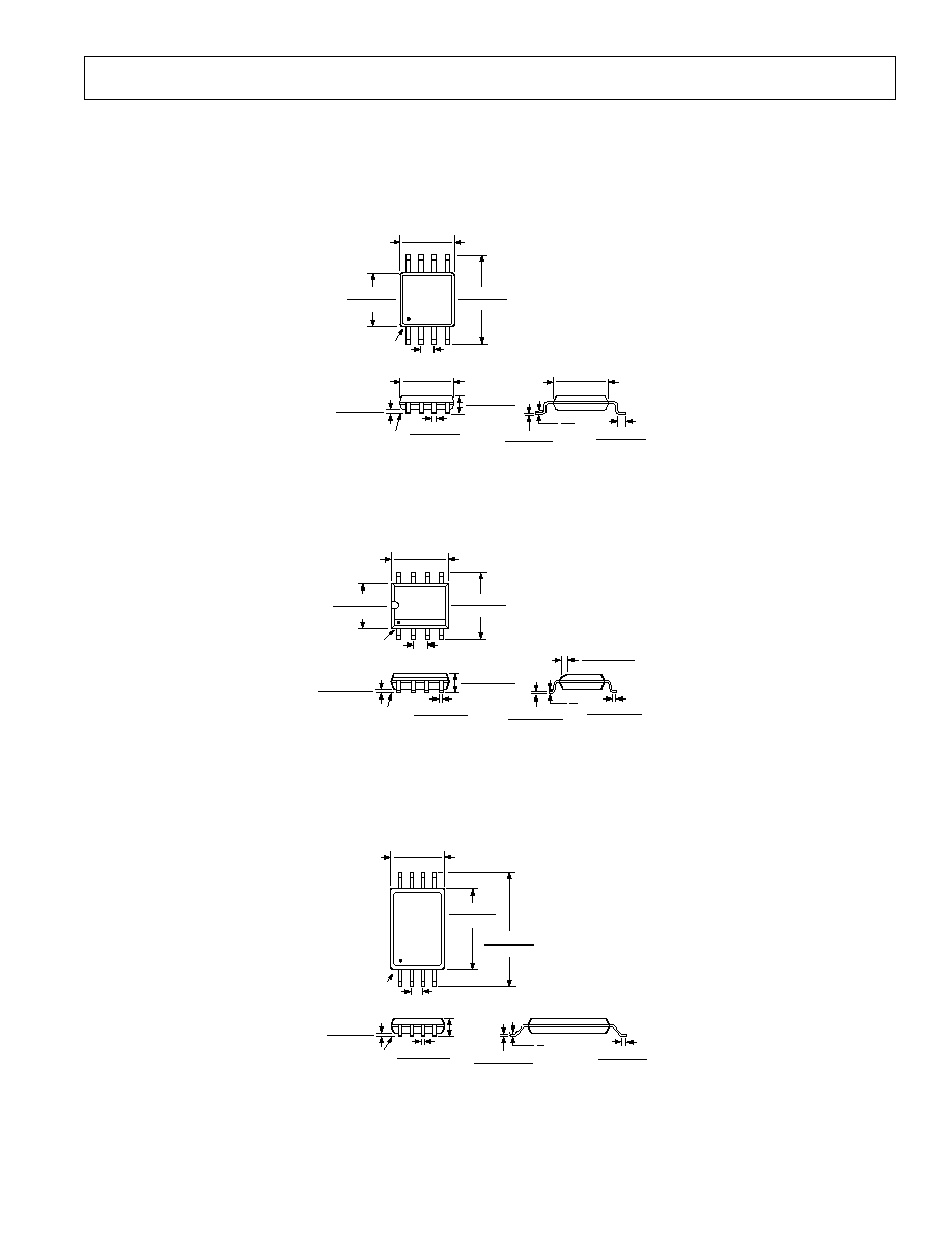
8-Lead MSOP
(RM-8)
0.011 (0.28)
0.003 (0.08)
0.028 (0.71)
0.016 (0.41)
33
27
0.120 (3.05)
0.112 (2.84)
8
5
4
1
0.122 (3.10)
0.114 (2.90)
0.199 (5.05)
0.187 (4.75)
PIN 1
0.0256 (0.65) BSC
0.122 (3.10)
0.114 (2.90)
SEATING
PLANE
0.006 (0.15)
0.002 (0.05)
0.018 (0.46)
0.008 (0.20)
0.043 (1.09)
0.037 (0.94)
0.120 (3.05)
0.112 (2.84)
8-Lead SOIC
(R-8)
0.0098 (0.25)
0.0075 (0.19)
0.0500 (1.27)
0.0160 (0.41)
8
0
0.0196 (0.50)
0.0099 (0.25)
45
8
5
4
1
0.1968 (5.00)
0.1890 (4.80)
0.2440 (6.20)
0.2284 (5.80)
PIN 1
0.1574 (4.00)
0.1497 (3.80)
0.0500 (1.27)
BSC
0.0688 (1.75)
0.0532 (1.35)
SEATING
PLANE
0.0098 (0.25)
0.0040 (0.10)
0.0192 (0.49)
0.0138 (0.35)
8-Lead TSSOP
(RU-8)
8
5
4
1
0.256 (6.50)
0.246 (6.25)
0.177 (4.50)
0.169 (4.30)
PIN 1
0.0256 (0.65)
BSC
0.122 (3.10)
0.114 (2.90)
SEATING
PLANE
0.006 (0.15)
0.002 (0.05)
0.0118 (0.30)
0.0075 (0.19)
0.0433
(1.10)
MAX
0.0079 (0.20)
0.0035 (0.090)
0.028 (0.70)
0.020 (0.50)
8
0
OUTLINE DIMENSIONS
Dimensions shown in inches and (mm).

REV. C
OP777/OP727/OP747
≠14≠
14-Lead SOIC
(R-14)
14
8
7
1
0.2440 (6.20)
0.2284 (5.80)
0.1574 (4.00)
0.1497 (3.80)
PIN 1
0.3444 (8.75)
0.3367 (8.55)
0.050 (1.27)
BSC
SEATING
PLANE
0.0098 (0.25)
0.0040 (0.10)
0.0192 (0.49)
0.0138 (0.35)
0.0688 (1.75)
0.0532 (1.35)
8
0
0.0196 (0.50)
0.0099 (0.25)
45
0.0500 (1.27)
0.0160 (0.41)
0.0099 (0.25)
0.0075 (0.19)
14-Lead TSSOP
(RU-14)
14
8
7
1
0.256 (6.50)
0.246 (6.25)
0.177 (4.50)
0.169 (4.30)
PIN 1
0.201 (5.10)
0.193 (4.90)
SEATING
PLANE
0.006 (0.15)
0.002 (0.05)
0.0118 (0.30)
0.0075 (0.19)
0.0256
(0.65)
BSC
0.0433 (1.10)
MAX
0.0079 (0.20)
0.0035 (0.090)
0.028 (0.70)
0.020 (0.50)
8
0

REV. C
OP777/OP727/OP747
≠15≠
Revision History
Location
Page
Data Sheet changed from REV. B to REV. C.
Addition of text to APPLICATIONS section
. . . . . . . . . . . . . . . . . . . . . . . . . . . . . . . . . . . . . . . . . . . . . . . . . . . . . . . . . . . . . . .
1
Addition of 8-Lead SOIC (R-8) package
. . . . . . . . . . . . . . . . . . . . . . . . . . . . . . . . . . . . . . . . . . . . . . . . . . . . . . . . . . . . . . . . . .
1
Addition of text to GENERAL DESCRIPTION . . . . . . . . . . . . . . . . . . . . . . . . . . . . . . . . . . . . . . . . . . . . . . . . . . . . . . . . . . . . .
1
Addition of package to ORDERING GUIDE
. . . . . . . . . . . . . . . . . . . . . . . . . . . . . . . . . . . . . . . . . . . . . . . . . . . . . . . . . . . . . . .
2

≠16≠
CO2051
≠
0
≠
9/01(C)
PRINTED IN U.S.A.


