 | ÐлекÑÑоннÑй компоненÑ: OP97F | СкаÑаÑÑ:  PDF PDF  ZIP ZIP |
/home/web/htmldatasheet/RUSSIAN/html/ad/184157
REV. D
Information furnished by Analog Devices is believed to be accurate and
reliable. However, no responsibility is assumed by Analog Devices for its
use, nor for any infringements of patents or other rights of third parties that
may result from its use. No license is granted by implication or otherwise
under any patent or patent rights of Analog Devices.
a
OP97
One Technology Way, P.O. Box 9106, Norwood, MA 02062-9106, U.S.A.
Tel: 781/329-4700
www.analog.com
Fax: 781/326-8703
© Analog Devices, Inc., 2002
Low-Power, High-Precision
Operational Amplifier
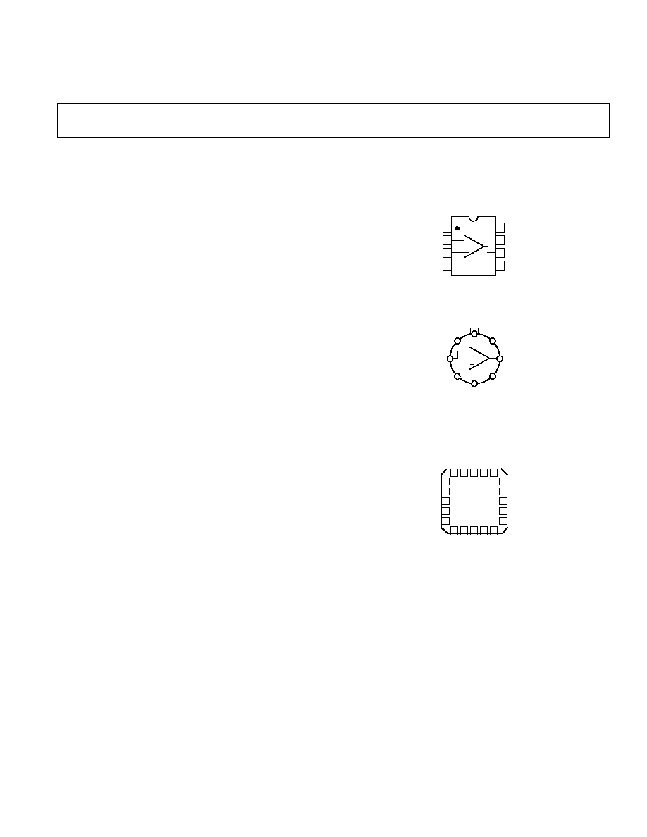
PIN CONNECTIONS
Epoxy Mini-DIP (P Suffix)
8-Pin Cerdip
(Z Suffix)
8-Pin SO (S Suffix)
1
2
3
4
8
7
6
5
OP97
NULL
OVER
COMP
OUT
V+
NULL
IN
+IN
V
TO-99 ( J Suffix)
NULL 1
IN 2
+IN 3
4
V (CASE)
5 OVER
COMP
6 OUT
7 V+
NULL
8
OP97ARC/883 LCC
(RC Suffix)
4
5
6
7
8
18
17
16
15
14
20 19
1
2
3
9
10 11 12 13
NC
IN
NC
+IN
NC
NC
V+
NC
OUT
NC
NC
V
NC
NC
NC
NC
V
OS
NC
NC
NC = NO CONNECT
V
OS
FEATURES
Low Supply Current: 600
A Max
OP07 Type Performance
Offset Voltage: 20
V Max
Offset Voltage Drift: 0.6
V/ C Max
Very Low Bias Current
25 C: 100 pA Max
55 C to +125 C: 250 pA Max
High Common-Mode Rejection: 114 dB Min
Extended Industrial Temperature Range: 40 C to +85 C
Available In Die Form
GENERAL DESCRIPTION
The OP97 is a low power alternative to the industry-standard
OP07 precision amplifier. The OP97 maintains the standards of
performance set by the OP07 while utilizing only 600
µ
A supply
current, less than 1/6 that of an OP07. Offset voltage is an
ultralow 25
µ
V, and drift over temperature is below 0.6
µ
V/
°
C.
External offset trimming is not required in the majority of circuits.
Improvements have been made over OP07 specifications in
several areas. Notable is bias current, which remains below
250 pA over the full military temperature range. The OP97 is
ideal for use in precision long-term integrators or sample-and-
hold circuits that must operate at elevated temperatures.
Common-mode rejection and power supply rejection are also
improved with the OP97, at 114 dB minimum over wider
ranges of common-mode or supply voltage. Outstanding
PSR, a supply range specified from
±
2.25 V to
±
20 V and the
OP97's minimal power requirements combine to make the
OP97 a preferred device for portable and battery-powered
instruments.
The OP97 conforms to the OP07 pinout, with the null potenti-
ometer connected between Pins 1 and 8 with the wiper to V+.
The OP97 will upgrade circuit designs using 725, OP05, OP07,
OP12, and 1012 type amplifiers. It may replace 741-type ampli-
fiers in circuits without nulling or where the nulling circuitry has
been removed.
REV. D
2
OP97SPECIFICATIONS
ELECTRICAL CHARACTERISTICS
OP97A/E
OP97F
Parameter
Symbol
Conditions
Min
Typ
Max
Min
Typ
Max
Unit
Input Offset Voltage
V
OS
10
25
30
75
µ
V
Long-Term Offset
Voltage Stability
V
OS
/Time
0.3
0.3
µ
V/Month
Input Offset Current
I
OS
30
100
30
150
pA
Input Bias Current
I
B
±
30
±
100
±
30
±
150
pA
Input Noise Voltage
e
n
p-p
0.1 Hz to 10 Hz
0.5
0.5
µ
V p-p
Input Noise Voltage Density e
n
f
O
= 10 Hz
2
17
30
17
30
nV/
Hz
f
O
= 1000 Hz
3
14
22
14
22
nV/
Hz
Input Noise Current Density i
n
f
O
= 10 Hz
20
20
fA/
Hz
Large-Signal Voltage Gain
A
VO
V
O
=
±
10 V; R
L
= 2 k
300
2000
200
2000
V/mV
Common-Mode Rejection
CMR
V
CM
=
±
13.5 V
114
132
110
132
dB
Power-Supply Rejection
PSR
V
S
=
±
2 V to
±
20 V
114
132
110
132
dB
Input Voltage Range
IVR
(Note 1)
±
13.5
±
14.0
±
13.5
±
14.0
V
Output Voltage Swing
V
O
R
L
= 10 k
±
13
±
14
±
13
±
14
V
Slew Rate
SR
0.1
0.2
0.1
0.2
V/
µ
s
Differential Input Resistance R
IN
(Note 4)
30
30
M
Closed-Loop Bandwidth
BW
A
VCL
= +1
0.4
0.9
0.4
0.9
MHz
Supply Current
I
SY
380
600
380
600
µ
A
Supply Voltage
V
S
Operating Range
±
2
±
15
±
20
±
2
±
15
±
20
V
NOTES
1
Guaranteed by CMR test.
2
10 Hz noise voltage density is sample tested. Devices 100% tested for noise are available on request.
3
Sample tested.
4
Guaranteed by design.
Specifications subject to change without notice.
ELECTRICAL CHARACTERISTICS
OP97A/E
OP97F
Parameter
Symbol
Conditions
Min
Typ
Max
Min
Typ
Max
Unit
Input Offset Voltage
VOS
25
60
60
200
µ
V
Average Temperature
TCV
OS
S-Package
0.2
0.6
0.3
2.0
µ
V/
°
C
Coefficient of V
OS
0.3
Input Offset Current
I
OS
60
250
80
750
pA
Average Temperature
TCI
OS
0.4
2.5
0.6
7.5
pA/
°
C
Coefficient of I
OS
Input Bias Current
I
B
±
60
±
250
±
80
±
750
pA
Average Temperature
Coefficient of I
B
TCI
B
0.4
2.5
0.6
7.5
pA/
°
C
Large Signal Voltage Gain
A
VO
V
O
= +10 V; R
L
= 2 k
200
1000
150
1000
V/mV
Common-Mode Rejection
CMR
V
CM
=
±
13.5 V
108
128
108
128
dB
Power Supply Rejection
PSR
V
S
=
±
2.5 V to
±
20 V
108
126
108
128
dB
Input Voltage Range
IVR
(Note 1)
±
13.5
±
14.0
±
13.5
±
14.0
V
Output Voltage Swing
V
O
R
L
= 10 k
±
13
±
14
±
13
±
14
V
Slew Rate
SR
0.05
0.15
0.05
0.15
V/
µ
s
Supply Current
I
SY
400
800
400
800
µ
A
Supply Voltage
V
S
Operating Range
±
2.5
±
15
±
20
±
2.5
±
15
±
20
V
NOTES
1
Guaranteed by CMR test.
Specifications subject to change without notice.
(@ V
S
= 15 V, V
CM
= 0 V, T
A
= 25 C, unless otherwise noted.)
(@ V
S
= 15 V, V
CM
= 0 V, 40 C
T
A
+85 C for the OP97E/F and 55 C
T
A
+125 C
for the OP97A, unless otherwise noted.)
REV. D
OP97
3
CAUTION
ESD (electrostatic discharge) sensitive device. Electrostatic charges as high as 4000 V readily
accumulate on the human body and test equipment and can discharge without detection. Although
the OP97 features proprietary ESD protection circuitry, permanent damage may occur on devices
subjected to high-energy electrostatic discharges. Therefore, proper ESD precautions are
recommended to avoid performance degradation or loss of functionality.
WARNING!
ESD SENSITIVE DEVICE
ABSOLUTE MAXIMUM RATINGS
1
Supply Voltage . . . . . . . . . . . . . . . . . . . . . . . . . . . . . . .
±
20 V
Input Voltage
2
. . . . . . . . . . . . . . . . . . . . . . . . . . . . . . .
±
20 V
Differential Input Voltage
3
. . . . . . . . . . . . . . . . . . . . . .
±
1 V
Differential Input Current
3
. . . . . . . . . . . . . . . . . . . .
±
10 mA
Output Short-Circuit Duration . . . . . . . . . . . . . . . . Indefinite
Operating Temperature Range
OP97A (J, Z, RC) . . . . . . . . . . . . . . . . . . . 55
°
C to +125
°
C
OP97E, F (J, P, Z, S) . . . . . . . . . . . . . . . . . 40
°
C to +85
°
C
Storage Temperature Range . . . . . . . . . . . . 65
°
C to +150
°
C
Junction Temperature Range . . . . . . . . . . . . 65
°
C to +150
°
C
Lead Temperature (Soldering, 60 sec) . . . . . . . . . . . . 300
°
C
Package Type
JA
4
JC
Unit
TO-99 (J)
150
18
°
C/W
8-Lead Hermetic DIP (Z)
148
16
°
C/W
8-Lead Plastic DIP (P)
103
43
°
C/W
8-Lead SO (S)
158
43
°
C/W
20-Contact LCC (RC)
98
98
°
C/W
NOTES
1
Absolute maximum ratings apply to both DICE and packaged parts, unless
otherwise noted.
2
For supply voltages less than
±
20 V, the absolute maximum input voltage is equal
to the supply voltage.
3
The OP97's inputs are protected by back-to-back diodes. Current-limiting resis-
tors are not used in order to achieve low noise. Differential input voltages greater
than 1 V will cause excessive current to flow through the input protection diodes
unless limiting resistance is used.
4
JA
is specified for worst case mounting conditions, i.e.,
JA
is specified for device
in socket for TO, cerdip, and P-DIP packages;
JA
is specified for device soldered
to printed circuit board for SO package.
ORDERING GUIDE
Temperature
Package
Model
Range
Option
1
OP97AZ
55
°
C to +125
°
C
8-Pin Cerdip
OP97ARC/883
2
55
°
C to +125
°
C
20-Contact LCC
OP97EJ
40
°
C to +85
°
C
TO-99
OP97EZ
40
°
C to +85
°
C
8-Pin Cerdip
OP97EP
40
°
C to +85
°
C
8-Pin Plastic DIP
OP97FJ
40
°
C to +85
°
C
TO-99
OP97FZ
40
°
C to +85
°
C
8-Pin Cerdip
OP97FP
40
°
C to +85
°
C
8-Pin Plastic DIP
OP97FS
40
°
C to +85
°
C
8-Pin SOIC
OP97FS-REEL
40
°
C to +85
°
C
8-Pin SOIC
OP97FS-REEL7
40
°
C to +85
°
C
8-Pin SOIC
NOTES
1
For outline information see Package Information section.
2
For devices processed in total compliance to MIL-STD-883, add /883 after
part number. Consult factory for /883 data sheet.
REV. D
OP97
4
DIE CHARACTERISTICS
WAFER TEST LIMITS
Parameter
Symbol
Condition
Limit
Unit
Input Offset Voltage
V
OS
250
µ
V Max
Input Offset Current
I
OS
150
pA Max
Input Bias Current
I
B
±
150
pA Max
Large Signal Voltage Gain
A
VO
V
OUT
=
±
10 V, R
L
= 2 k
120
V/mV Min
Common-Mode Rejection
CMR
V
CM
=
±
13.5
110
dB Min
Power Supply Rejection
PSR
V
S
=
±
2 V to
±
20 V
110
dB Min
Input Voltage Range
IVR
(Note 1)
±
13.5
V Min
Output Voltage Swing
V
O
R
L
= 10 k
±
13
V Min
Slew Rate
SR
0.1
V/
µ
s Min
Supply Current
I
SY
No Load
600
µ
A Max
NOTES
1
Guaranteed by CMR test.
Electrical tests are performed at wafer probe to the limits shown. Due to variations in assembly methods and normal yield loss, yield after packaging is not guaranteed
for standard product dice. Consult factory to negotiate specifications based on dice lot qualification through sample lot assembly and testing.
4
3
2
1
8
7
6
5
1. OUTPUT
2. +VS
3. OFFSET NULL
4. OFFSET NULL
5. INPUT
6. +INPUT
7. VS
8. OVER COMP
DIE SIZE 0.063 0.074 INCH, 4,662 SQ. mils
(1.60 1.88 mm, 3.01 SQ. mm)
(@ V
S
= 15 V, V
CM
= 0 V, T
A
= 25 C, unless otherwise noted.)
REV. D
5
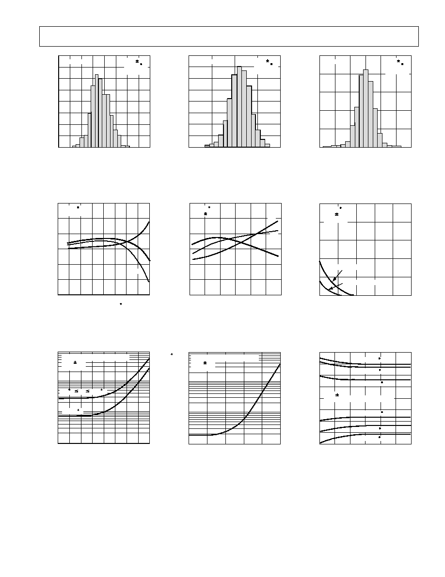
Typical Performance CharacteristicsOP97
INPUT OFFSET VOLTAGE V
NUMBER OF UNITS
0
40
100
200
300
400
20
0
20
40
1894 UNITS
V
S
= 15V
T
A
= 25 C
V
CM
= 0V
TPC 1. Typical Distribution of Input
Offset Voltage
TEMPERATURE C
INPUT CURRENT - pA
60
75
25
0
25
50
50
75
T
A
= 25 C
V
CM
= 0V
I
B
I
OS
I
B
+
40
20
0
20
40
60
100
125
TPC 4. Input Bias, Offset Current
vs. Temperature
SOURCE RESISTANCE
EFFECTIVE OFFSET VOLTAGE
V
1000
1
1k
100
10
3k
10k
30k 100k
1M
300k
3M
10M
BALANCED OR UNBALANCED
V
S
= 15V
V
CM
= 0V
55 C T
A
+125 C
T
A
= 25 C
TPC 7. Effective Offset Voltage vs.
Source Resistance
INPUT BIAS CURRENT pA
NUMBER OF UNITS
0
100
100
200
300
400
50
0
50
100
1920 UNITS
V
S
= 15V
T
A
= 25 C
V
CM
= 0V
TPC 2. Typical Distribution of Input
Bias Current
COMMON-MODE VOLTAGE Volts
INPUT CURRENT - pA
60
15
5
0
5
10
10
15
T
A
= 25 C
V
S
= 15V
I
B
I
OS
I
B
+
40
20
0
20
40
60
TPC 5. Input Bias, Offset Current
vs. Common-Mode Voltage
SOURCE RESISTANCE
EFFECTIVE OFFSET VOLTAGE DRIFT
V/
C
100
0.1
1k
10
1
10k
100k
1M
10M
BALANCED OR UNBALANCED
V
S
= 15V
V
CM
= 0V
100M
TPC 8. Effective TCV
OS
vs. Source
Resistance
INPUT OFFSET CURRENT pA
NUMBER OF UNITS
0
60
100
200
300
400
20
0
20
40
1894 UNITS
V
S
= 15V
T
A
= 25 C
V
CM
= 0V
40
60
500
TPC 3. Typical Distribution of Input
Offset Current
TIME AFTER POWER APPLIED Minutes
DEVIATION FROM FINAL VALUE
V
0
0
1
2
3
4
2
3
4
5
T
A
= 25 C
V
S
= 15V
V
CM
= 0V
1
5
J PACKAGES
Z, P PACKAGES
TPC 6. Input Offset Voltage
Warm-Up Drift
TIME FROM OUTPUT SHORT Minutes
SHORT CIRCUIT CURRENT - mA
20
0
15
10
5
10
20
1
2
3
0
15
5
V
S
= 15V
OUTPUT SHORTED TO GROUND
T
A
= +125 C
T
A
= +25 C
T
A
= 55 C
T
A
= +125 C
T
A
= +25 C
T
A
= 55 C
TPC 9. Short Circuit Current vs.
Time, Temperature
REV. D
OP97
6
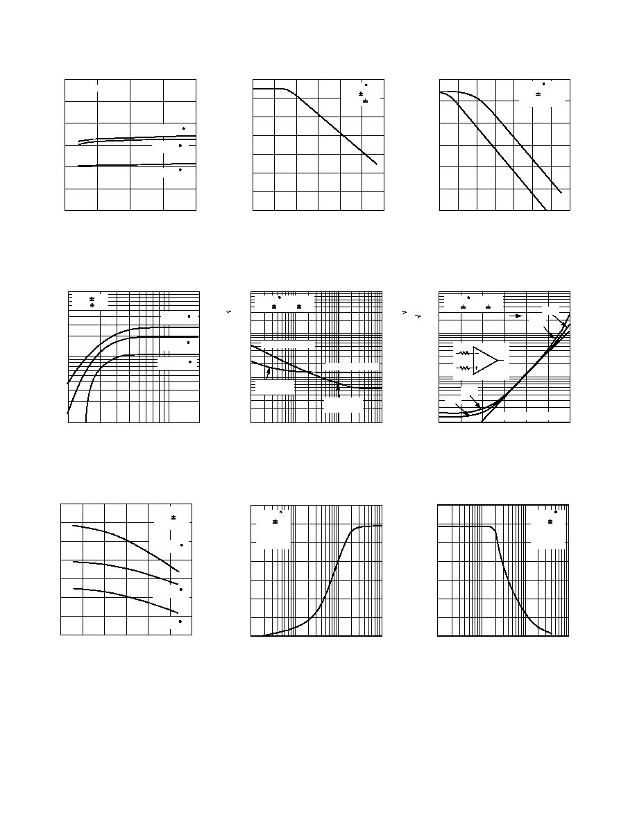
SUPPLY VOLTAGE V
SUPPLY CURRENT
A
300
0
325
375
400
450
5
NO LOAD
T
A
= +125 C
T
A
= 55 C
T
A
= +25 C
350
425
10
15
20
TPC 10. Supply Current vs. Supply
Voltage
LOAD RESISTANCE k
OPEN-LOOP GAIN
V/mV
10000
1
1000
100
2
5
10
20
T
A
= +125 C
T
A
= 55 C
T
A
= +25 C
V
S
= 15V
V
O
= 10V
TPC 13. Open-Loop Gain vs. Load
Resistance
OUTPUT VOLTAGE V
DIFFERENTIAL INPUT VOLTAGE
10
V/DIV
15
5
0
5
10
R
L
= 10k
V
S
= 15V
V
CM
= 0V
10
15
T
A
= +125 C
T
A
= 55 C
T
A
= +25 C
Figure 16. Open-Loop Gain Linearity
FREQUENCY Hz
COMMON-MODE REJECTION
dB
0
1
100
10
100
1k
10k
T
A
= 25 C
V
S
= 15V
V
CM
= 10V
20
40
60
80
120
140
100k
1M
TPC 11. Common-Mode Rejection
vs. Frequency
FREQUENCY Hz
100
1k
10
1
10k
100k
1M
10M
100M
CURRENT NOISE
1/f CORNER
120Hz
VOLTAGE NOISE
1/f CORNER
2.5Hz
T
A
= 25 C
V
S
= 2V TO 20V
1000
VOLTAGE NOISE DENSITY
nV/
Hz
CURRENT NOISE DENSITY
fV/
Hz
100
10
1
1000
TPC 14. Noise Density vs.
Frequency
LOAD RESISTANCE
OUTPUT SWING
V p-p
35
1
10
30
10k
1k
100
T
A
= 25 C
V
S
= 15V
A
VCL
= +1
1% THD
f
O
= 1kHz
25
20
15
10
5
TPC 17. Maximum Output Swing
vs. Load Resistance
FREQUENCY Hz
POWER-SUPPLY REJECTION
dB
20
0.1
40
60
80
100
10
100
1k
10k
PSR
T
A
= 25 C
V
S
= 15V
V
S
= 10V pp
1
100k
140
+PSR
120
1M
TPC 12. Power-Supply Rejection
vs. Frequency
SOURCE RESISTANCE
10
0.01
10
2
1
0.1
T
A
= 25 C
V
S
= 2V TO 20V
TOTAL NOISE DENSITY
V/
Hz
RESISTOR NOISE
1kHz
10Hz
R
R
R
S
= 2R
10
3
10
4
10
5
10
6
10
7
10
8
1kHz
10Hz
TPC 15. Total Noise Density vs.
Source Resistance
FREQUENCY Hz
OUTPUT SWING
V p-p
35
1
30
100k
1k
100
T
A
= 25 C
V
S
= 15V
A
VCL
= 1
1% THD
R
l
= 10k
25
20
15
10
5
10k
TPC 18. Maximum Output Swing
vs. Frequency
REV. D
7
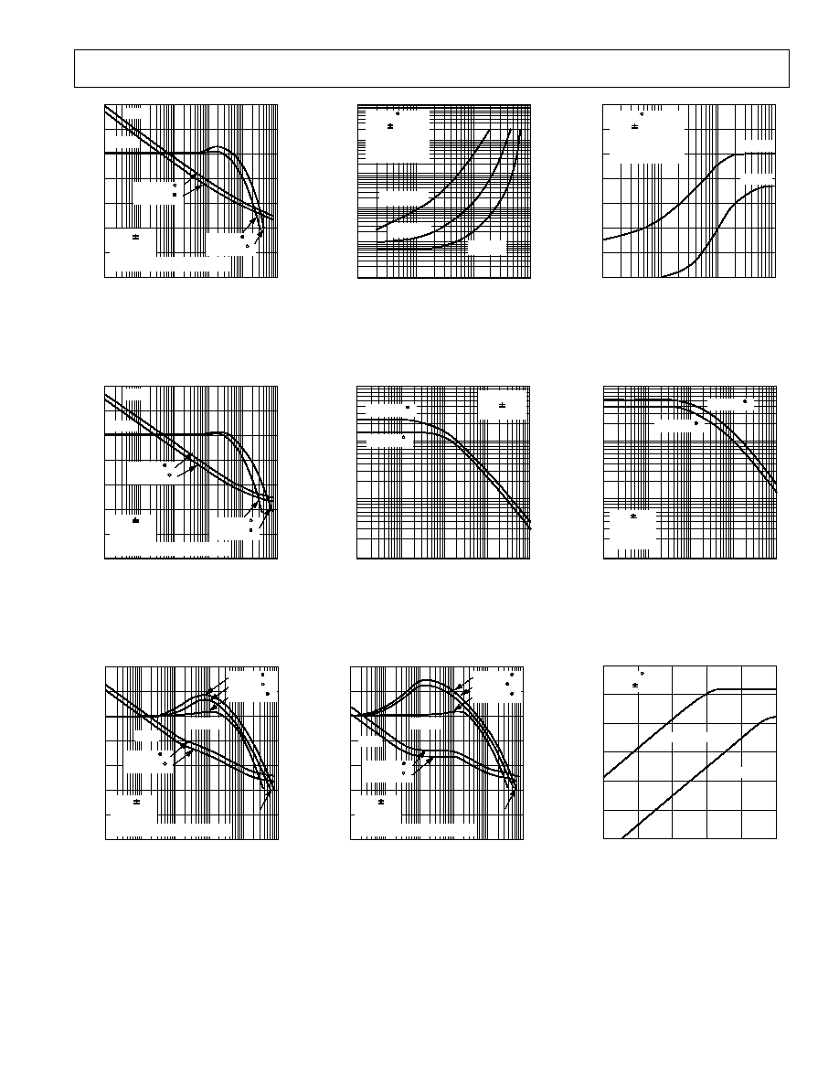
Typical Performance CharacteristicsOP97
FREQUENCY Hz
OPEN-LOOP GAIN
dB
80
60
100
60
10M
1k
100k
40
10k
1M
40
20
0
20
PHASE
PHASE SHIFT
Degrees
225
180
135
90
T
A
= +125 C
T
A
= 55 C
T
A
= 55 C
T
A
= +125 C
V
S
= 15V
C
L
= 20pF
R
L
= 1M
100pF OVERCOMPENSATION
GAIN
V
S
= 15V
C
L
= 20pF
R
L
= 1M
100pF OVERCOMPENSATION
TPC 19. Open-Loop Gain, Phase vs.
Frequency (C
OC
= 0 pF)
FREQUENCY Hz
OPEN-LOOP GAIN
dB
80
60
100
60
10M
1k
100k
40
10k
1M
40
20
0
20
PHASE
PHASE SHIFT
Degrees
225
180
135
90
T
A
= +125 C
T
A
= 55 C
GAIN
V
S
= 15V
C
L
= 20pF
R
L
= 1M
100pF OVERCOMPENSATION
T
A
= 55 C
T
A
= +125 C
TPC 22. Open-Loop Gain, Phase vs.
Frequency (C
OC
= 100 pF)
FREQUENCY Hz
OPEN-LOOP GAIN
dB
80
60
100
60
10M
1k
100k
40
10k
1M
40
20
0
20
PHASE
PHASE SHIFT
Degrees
225
180
135
90
T
A
= 55 C
T
A
= +25 C
T
A
= +125 C
GAIN
V
S
= 15V
C
L
= 20pF
R
L
= 1M
100pF OVERCOMPENSATION
T
A
= 55 C
T
A
= +125 C
TPC 25. Open-Loop Gain, Phase vs.
Frequency (C
OC
= 1000 pF)
FREQUENCY Hz
THD + N
%
0.0001
10
10k
1k
100
T
A
= 25 C
V
S
= 15V
R
L
= 10k
1% THD
V
OUT
= 3V RMS
A
VCL
= 100
A
VCL
= 10
A
VCL
= 1
0.001
0.01
0.1
1
10
TPC 20. Total Harmonic Distortion
Plus Noise vs. Frequency
OVERCOMPENSATION CAPACITOR pF
0.1
1
0.01
0.001
10
100
10000
1
SLEW RATE
V/
s
R
l
= 10k
V
S
= 15V
C
L
= 100pF
T
A
= +125 C
T
A
= 55 C
1000
TPC 23. Slew Rate vs. Over-
compensation
FREQUENCY Hz
OPEN-LOOP GAIN
dB
80
60
100
60
10M
1k
100k
40
10k
1M
40
20
0
20
PHASE
PHASE SHIFT
Degrees
225
180
135
90
T
A
= +125 C
T
A
= +25 C
T
A
= +125 C
GAIN
V
S
= 15V
C
L
= 20pF
R
L
= 1M
100pF OVERCOMPENSATION
T
A
= +125 C
T
A
= 55 C
TPC 26. Open-Loop Gain, Phase vs.
Frequency (C
OC
= 10,000 pF)
LOAD CAPACITANCE pF
OVERSHOOT
%
70
0
10
60
10000
1000
100
T
A
= 25 C
V
S
= 15V
A
VCL
= +1
V
OUT
= 100mV p-p
C
OC
= 0pF
50
40
30
20
10
+EDGE
EDGE
TPC 21. Small Signal Overshoot vs.
Capacitive Load
OVERCOMPENSATION CAPACITOR pF
100
1
10
1
10
100
10000
1000
GAIN-BANDWIDTH
kHz
V
S
= 15V
C
L
= 20pF
R
L
= 1M
A
V
= 100
T
A
= +125 C
T
A
= 55 C
1000
TPC 24. Gain Bandwidth Product vs.
Overcompensation
FREQUENCY Hz
OUTPUT IMPEDANCE
0.001
10
100
1k
10k
T
A
= 25 C
V
S
= 15V
1
A
VCL
= 1000
100k
A
VCL
= 1
0.01
0.1
1
10
100
1000
TPC 27. Closed-Loop Output Resis-
tance vs. Frequency
REV. D
OP97
8
APPLICATIONS INFORMATION
The OP97 is a low power alternative to the industry standard
precision op amp, the OP07. The OP97 may be substituted
directly into OP07, OP77, 725, OP05, 112/312, and 1012 sock-
ets with improved performance and/or less power dissipation,
and may be inserted into sockets conforming to the 741 pinout
if nulling circuitry is not used. Generally, nulling circuitry used
with earlier generation amplifiers is rendered superfluous by the
OP97's extremely low offset voltage, and may be removed with-
out compromising circuit performance.
Extremely low bias current over the full military temperature
range makes the OP97 attractive for use in sample-and-hold
amplifiers, peak detectors, and log amplifiers that must operate
over a wide temperature range. Balancing input resistances is
not necessary with the OP97. Offset voltage and TCV
OS
are
degraded only minimally by high source resistance, even when
unbalanced.
The input pins of the OP97 are protected against large differen-
tial voltage by back-to-back diodes. Current-limiting resistors
are not used so that low noise performance is maintained. If
differential voltages above
±
1 V are expected at the inputs,
series resistors must be used to limit the current flow to a maxi-
mum of 10 mA. Common-mode voltages at the inputs are not
restricted, and may vary over the full range of the supply volt-
ages used.
The OP97 requires very little operating headroom about the
supply rails, and is specified for operation with supplies as low
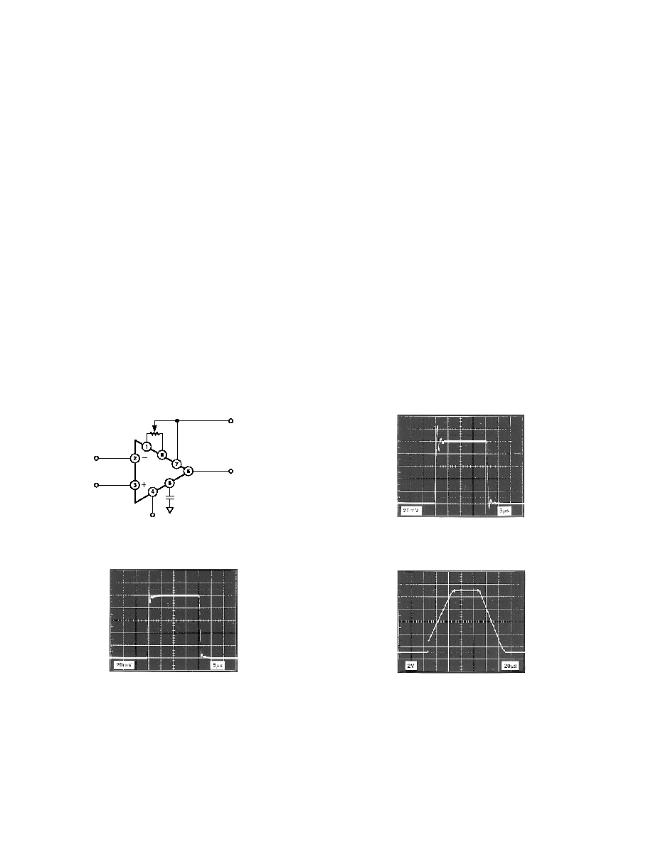
OP97
R
POT
= 5k TO 100k
C
OC
V
+V
Figure 1. Optional Input Offset Voltage Nulling
and Overcompensation Circuits
Figure 2. Small-Signal Transient Response
(C
LOAD
= 100 pF, A
VCL
= 1)
as
±
2 V. Typically, the common-mode range extends to within
one volt of either rail. The output typically swings to within one
volt of the rails when using a 10 k
load.
Offset nulling is achieved utilizing the same circuitry as an
OP07. A potentiometer between 5 k
and 100 k
is connected
between pins 1 and 8 with the wiper connected to the positive
supply. The trim range is between 300
µ
V and 850
µ
V, depend-
ing upon the internal trimming of the device.
AC PERFORMANCE
The OP97's ac characteristics are highly stable over its full
operating temperature range. Unity-gain small-signal response
is shown in Figure 2. Extremely tolerant of capacitive loading
on the output, the OP97 displays excellent response even with
1000 pF loads (Figure 3). In large-signal applications, the
input protection diodes effectively short the input to the output
during the transients if the amplifier is connected in the usual
unity-gain configuration. The output enters short-circuit current
limit, with the flow going through the protection diodes. Improved
large-signal transient response is obtained by using a feedback
resistor between the output and the inverting input. Figure 4
shows the large-signal response of the OP97 in unity gain with a
10 k
feedback resistor. The unity gain follower circuit is shown
in Figure 5.
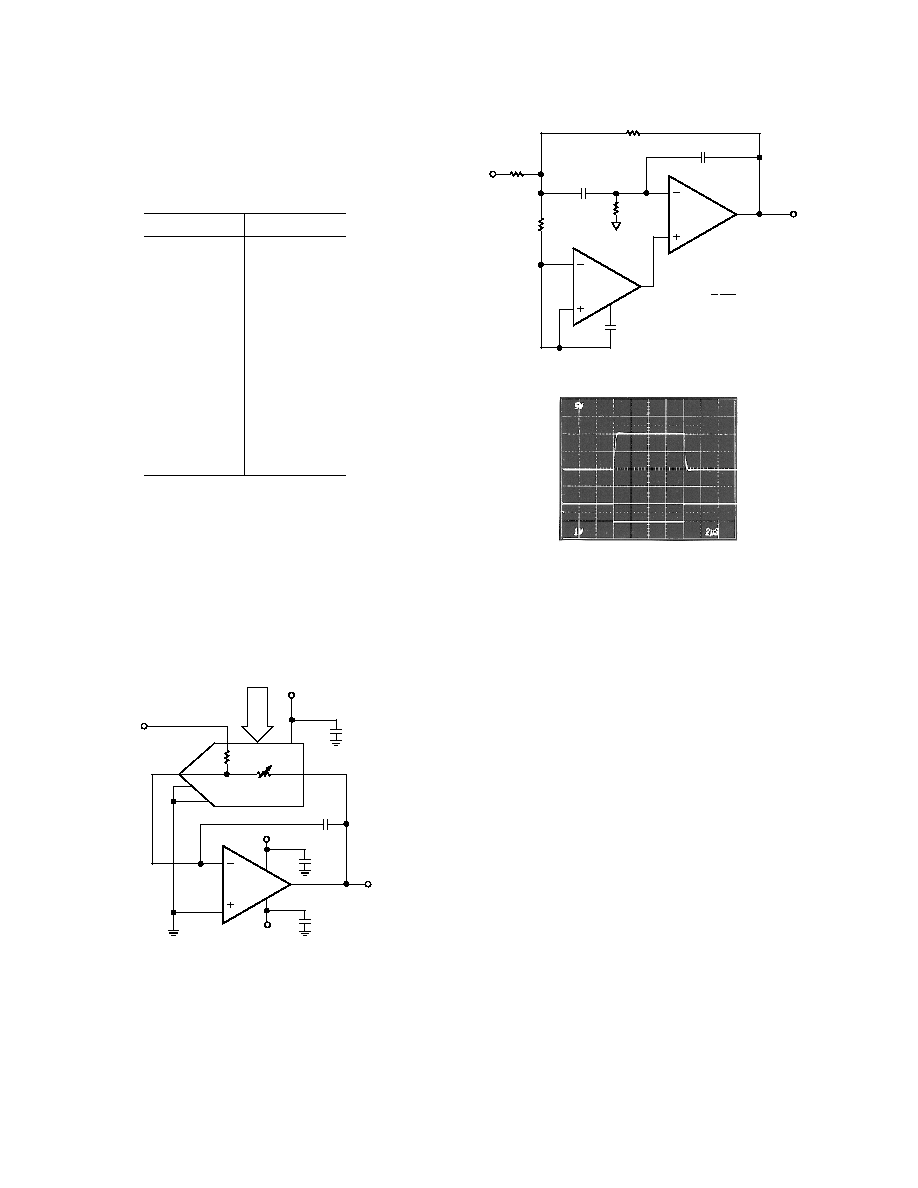
The overcompensation pin may be used to increase the phase
margin of the OP97, or to decrease gain-bandwidth product at
gains greater than 10.
Figure 3. Small-Signal Transient Response
(C
LOAD
= 1000 pF, A
VCL
= 1)
Figure 4. Large-Signal Transient Response (A
VCL
= 1)
REV. D
OP97
9
OP97
10k
V
OUT
2
3
6
V
IN
Figure 5. Unity-Gain Follower
Figure 6. Small-Signal Transient Response with Overcom-
pensation (C
LOAD
= 1000 pF, A
VCL
= 1, C
OC
= 220 pF)
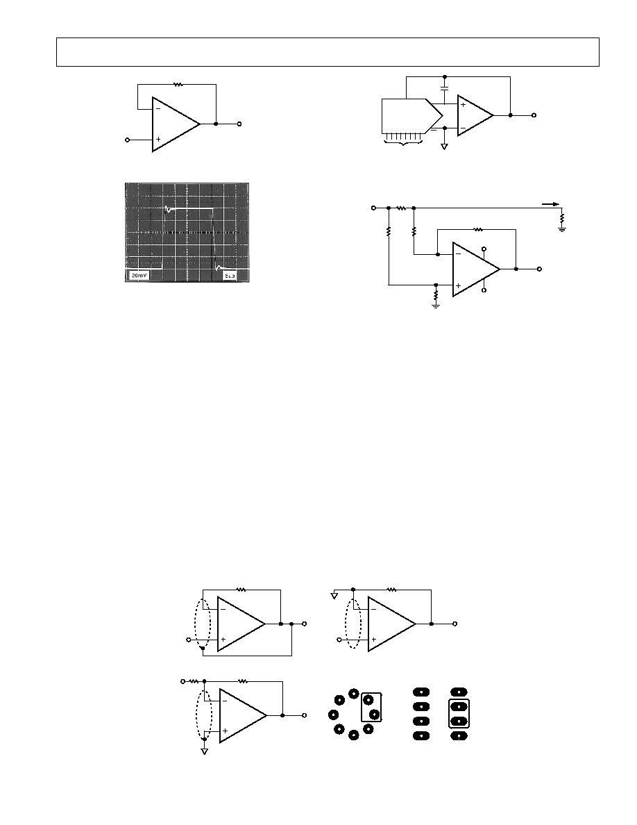
GUARDING AND SHIELDING
To maintain the extremely high input impedances of the OP97,
care must be taken in circuit board layout and manufacturing.
Board surfaces must be kept scrupulously clean and free of moisture.
Conformal coating is recommended to provide a humidity barrier.
Even a clean PC board can have 100 pA of leakage currents between
adjacent traces, so that guard rings should be used around the
inputs. Guard traces are operated at a voltage close to that on the
inputs, so that leakage currents become minimal. In nonin-
verting applications, the guard ring should be connected to the
common-mode voltage at the inverting input (Pin 2). In inverting
applications, both inputs remain at ground, so that the guard trace
should be grounded. Guard traces should be made on both sides
of the circuit board.
OP97
V
OUT
2
3
6
I
O
I
O
DIGITAL
INPUTS
30pF
R
FB
PM7548
Figure 7. DAC Output Amplifier
OP97
R5
10k
V
OUT
2
3
6
V1
R1
10k
R2
10k
R3
10k
R4
10k
15V
+15V
7
4
R
L
I
L
Figure 8. Current Monitor
High impedance circuitry is extremely susceptible to RF pickup,
line frequency hum, and radiated noise from switching power
supplies. Enclosing sensitive analog sections within grounded
shields is generally necessary to prevent excessive noise pickup.
Twisted-pair cable will aid in rejection of line frequency hum.
The OP97 is an excellent choice as an output amplifier for higher
resolution CMOS DACs. Its tightly trimmed offset voltage and
minimal bias current result in virtually no degradation of linear-
ity, even over wide temperature ranges.
Figure 8 shows a versatile monitor circuit that can typically
sense current at any point between the
±
15 V supplies. This
makes it ideal for sensing current in applications such as full
bridge drivers where bidirectional current is associated with large
common-mode voltage changes. The 114 dB CMRR of the OP97
makes the amplifier's contribution to common-mode error
negligible, leaving only the error due to the resistor ratio
inequality. Ideally, R2/R4 = R3/R5. This is best trimmed via R4
OP97
2
3
6
UNITY-GAIN FOLLOWER
OP97
2
3
6
NONINVERTING AMPLIFIER
OP97
2
3
6
INVERTING AMPLIFIER
1
8
1
8
TO-99
BOTTOM VIEW
MINI-DIP
BOTTOM VIEW
Figure 9. Guard Ring Layout and Connections
REV. D
OP97
10
The digitally programmable gain amplifier shown in Figure 10
has 12-bit gain resolution with 10-bit gain linearity over the
range of 1 to 1024. The low bias current of the OP97 main-
tains this linearity, while C1 limits the noise voltage bandwidth
allowing accurate measurement down to microvolt levels.
DIGITAL IN
GAIN (Av)
4095
1.00024
2048
2
1024
4
512
8
256
16
128
32
64
64
32
128
16
256
8
512
4
1024
2
2048
1
4096
0
OPEN LOOP
Many high-speed amplifiers suffer from less-than-perfect low-
frequency performance. A combination amplifier consisting of a
high precision, slow device like the OP97 and a faster device
such as the OP44 results in uniformly accurate performance
from dc to the high frequency limit of the OP44, which has a
gain-bandwidth product of 23 MHz. The circuit shown in Figure 11
accomplishes this, with the OP44 providing high frequency
amplification and the OP97 operating on low frequency signals
and providing offset correction. Offset voltage and drift of the
circuit are controlled by the OP97.
V
OUT
OP97
2
3
6
0.1 F
+15V
C1
220pF
17
16
PM7541
V
REF
R
FB
1
2
3
18
2.5mV TO 10V
RANGE DEPENDING
ON GAIN SETTING
V
IN
15V
0.1 F
+15V
I
OUT 1
I
OUT 2
0.1 F
Figure 10. Precision Programmable Gain Amplifier
OP44
V
OUT
2
3
6
OP97
2
3
6
R2
20k
5
10k
1 F
R1
2k
V
IN
0.1 F
10k
5pF
R2
R1
A
V
=
Figure 11. Combination High-Speed, Precision Amplifier
Figure 12. Combination Amplifier Transient Response
.
REV. D
OP97
11
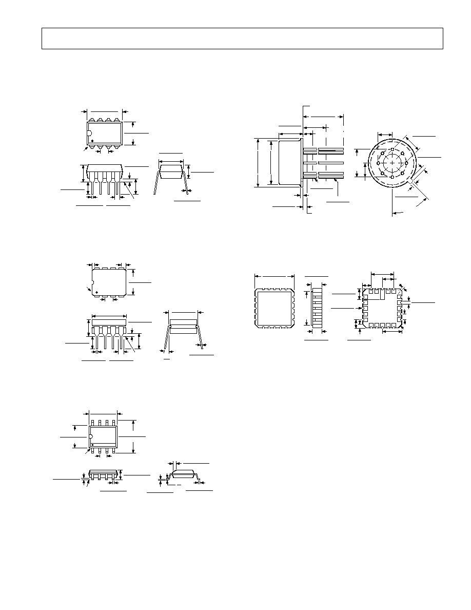
OUTLINE DIMENSIONS
Dimensions shown in inches and (mm).
8-Lead Plastic DIP
(N-8)
SEATING
PLANE
0.060 (1.52)
0.015 (0.38)
0.210
(5.33)
MAX
0.022 (0.558)
0.014 (0.356)
0.160 (4.06)
0.115 (2.93)
0.070 (1.77)
0.045 (1.15)
0.130
(3.30)
MIN
8
1
4
5
PIN 1
0.280 (7.11)
0.240 (6.10)
0.100 (2.54)
BSC
0.430 (10.92)
0.348 (8.84)
0.195 (4.95)
0.115 (2.93)
0.015 (0.381)
0.008 (0.204)
0.325 (8.25)
0.300 (7.62)
8-Pin Hermetic DIP
(Q-8)
1
4
8
5
0.310 (7.87)
0.220 (5.59)
PIN 1
0.005 (0.13)
MIN
0.055 (1.4)
MAX
0.100 (2.54) BSC
15°
0°
0.320 (8.13)
0.290 (7.37)
0.015 (0.38)
0.008 (0.20)
SEATING
PLANE
0.200 (5.08)
MAX
0.405 (10.29) MAX
0.150
(3.81)
MIN
0.200 (5.08)
0.125 (3.18)
0.023 (0.58)
0.014 (0.36)
0.070 (1.78)
0.030 (0.76)
0.060 (1.52)
0.015 (0.38)
8-Pin SOIC
(SO-8)
0.0098 (0.25)
0.0075 (0.19)
0.0500 (1.27)
0.0160 (0.41)
8
0
0.0196 (0.50)
0.0099 (0.25)
45
8
5
4
1
0.1968 (5.00)
0.1890 (4.80)
0.2440 (6.20)
0.2284 (5.80)
PIN 1
0.1574 (4.00)
0.1497 (3.80)
0.0500 (1.27)
BSC
0.0688 (1.75)
0.0532 (1.35)
SEATING
PLANE
0.0098 (0.25)
0.0040 (0.10)
0.0192 (0.49)
0.0138 (0.35)
8-Lead Metal Can
(H-08A)
0.250 (6.35) MIN
0.750 (19.05)
0.500 (12.70)
0.185 (4.70)
0.165 (4.19)
REFERENCE PLANE
0.050 (1.27) MAX
0.019 (0.48)
0.016 (0.41)
0.021 (0.53)
0.016 (0.41)
0.045 (1.14)
0.010 (0.25)
0.040 (1.02) MAX
BASE & SEATING PLANE
0.335 (8.51)
0.305 (7.75)
0.370 (9.40)
0.335 (8.51)
0.034 (0.86)
0.027 (0.69)
0.045 (1.14)
0.027 (0.69)
0.160 (4.06)
0.110 (2.79)
0.100 (2.54) BSC
6
2
8
7
5
4
3
1
0.200
(5.08)
BSC
0.100
(2.54)
BSC
45
°
BSC
20-Terminal Ceramic Leadless Chip Carrier (CLCC)
(E-20A)
TOP
VIEW
0.358 (9.09)
0.342 (8.69)
SQ
1
20
4
9
8
13
19
14
3
18
BOTTOM
VIEW
0.028 (0.71)
0.022 (0.56)
45° TYP
0.015 (0.38)
MIN
0.055 (1.40)
0.045 (1.14)
0.050 (1.27)
BSC
0.075 (1.91)
REF
0.011 (0.28)
0.007 (0.18)
R TYP
0.095 (2.41)
0.075 (1.90)
0.100 (2.54) BSC
0.200 (5.08)
BSC
0.150 (3.81)
BSC
0.075
(1.91)
REF
0.358
(9.09)
MAX
SQ
0.100 (2.54)
0.064 (1.63)
0.088 (2.24)
0.054 (1.37)

REV. D
12
C0029901/02(D)
PRINTED IN U.S.A.
OP97
Document Outline
- FEATURES
- GENERAL DESCRIPTION
- PIN CONNECTIONS
- SPECIFICATIONS
- ABSOLUTE MAXIMUM RATINGS
- ORDERING GUIDE
- DIE CHARACTERISTICS
- WAFER TEST LIMITS
- Typical Performance Characteristics
- APPLICATIONS INFORMATION
- AC PERFORMANCE
- GUARDING AND SHIELDING
- OUTLINE DIMENSIONS