 | ÐлекÑÑоннÑй компоненÑ: SSM2143 | СкаÑаÑÑ:  PDF PDF  ZIP ZIP |
Äîêóìåíòàöèÿ è îïèñàíèÿ www.docs.chipfind.ru
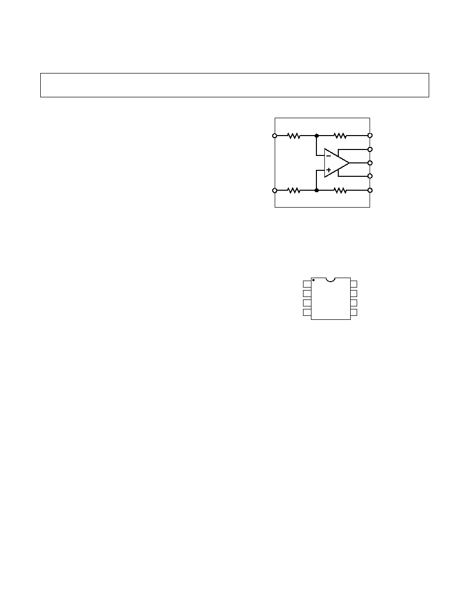
FUNCTIONAL BLOCK DIAGRAM
12k
12k
6k
6k
IN
+IN
SSM2143
V
OUT
REFERENCE
V+
V
SENSE
PIN CONNECTIONS
Epoxy Mini-DIP (P Suffix)
and
SOIC (S Suffix)
1
2
3
4
5
6
7
8
REF
IN
+IN
V
OP-482
NC
V+
SENSE
SSM2143
TOP VIEW
(NOT TO SCALE)
NC = NO CONNECT
V
OUT
REV. 0
Information furnished by Analog Devices is believed to be accurate and
reliable. However, no responsibility is assumed by Analog Devices for its
use, nor for any infringements of patents or other rights of third parties
which may result from its use. No license is granted by implication or
otherwise under any patent or patent rights of Analog Devices.
a
6 dB Differential
Line Receiver
SSM2143
One Technology Way, P.O. Box 9106, Norwood, MA 02062-9106, U.S.A.
Tel: 617/329-4700
Fax: 617/326-8703
FEATURES
High Common-Mode Rejection
DC: 90 dB typ
60 Hz: 90 dB typ
20 kHz: 85 dB typ
Ultralow THD: 0.0006% typ @ 1 kHz
Fast Slew Rate: 10 V/ s typ
Wide Bandwidth: 7 MHz typ (G = 1/2)
Two Gain Levels Available: G = 1/2 or 2
Low Cost
GENERAL DESCRIPTION
The SSM2143 is an integrated differential amplifier intended to
receive balanced line inputs in audio applications requiring a
high level of immunity from common-mode noise. The device
provides a typical 90 dB of common-mode rejection (CMR),
which is achieved by laser trimming of resistances to better than
0.005%.
Additional features of the device include a slew rate of 10 V/
µ
s
and wide bandwidth. Total harmonic distortion (THD) is less
than 0.004% over the full audio band, even while driving low
impedance loads. The SSM2143 input stage is designed to
handle input signals as large as +28 dBu at G = 1/2. Although
primarily intended for G = 1/2 applications, a gain of 2 can be
realized by reversing the +IN/IN and SENSE/REFERENCE
connections.
When configured for a gain of 1/2, the SSM2143 and SSM2142
Balanced Line Driver provide a fully integrated, unity gain
solution to driving audio signals over long cable runs. For
similar performance with G = 1, see SSM2141.
REV. 0
2
SSM2143SPECIFICATIONS
Parameter
Symbol
Conditions
Min
Typ
Max
Units
AUDIO PERFORMANCE
Total Harmonic Distortion Plus Noise
THD+N
V
IN
= 10 V rms, R
L
= 10 k
, f = 1 kHz
0.0006
%
Signal-to-Noise Ratio
SNR
0 dBu = 0.775 V rms, 20 kHz BW, RTI
107.3
dBu
Headroom
HR
Clip Point = 1% THD+N
+28.0
dBu
DYNAMIC RESPONSE
Slew Rate
SR
R
L
= 2 k
, C
L
= 200 pF
6
10
V/
µ
s
Small Signal Bandwidth
BW
3 dB
R
L
= 2 k
, C
L
= 200 pF
G = 1/2
7
MHz
G = 2
3.5
MHz
INPUT
Input Offset Voltage
V
IOS
V
CM
= 0 V, RTI, G = 2
1.2
0.05
+1.2
mV
Common-Mode Rejection
CMR
V
CM
=
±
10 V, RTO
f = dc
70
90
dB
f = 60 Hz
90
dB
f = 20 kHz
85
dB
f = 400 kHz
60
dB
Power Supply Rejection
PSR
V
S
=
±
6 V to
±
18 V
90
110
dB
Input Voltage Range
IVR
Common Mode
±
15
V
Differential
±
28
V
OUTPUT
Output Voltage Swing
V
O
R
L
= 2 k
±
13
±
14
V
Minimum Resistive Load Drive
2
k
Maximum Capacitive Load Drive
300
pF
Short Circuit Current Limit
I
SC
+45, 20
mA
GAIN
Gain Accuracy
0.1
0.03
0.1
%
REFERENCE INPUT
Input Resistance
18
k
Voltage Range
±
10
V
POWER SUPPLY
Supply Voltage Range
V
S
±
6
±
18
V
Supply Current
I
SY
V
CM
= 0 V, R
L
=
±
2.7
±
4.0
mA
Specifications subject to change without notice.
(V
S
= 15 V, 40 C
T
A
+85 C, G = 1/2, unless otherwise noted.
Typical specifications apply at T
A
= +25 C)
ABSOLUTE MAXIMUM RATINGS
Supply Voltage . . . . . . . . . . . . . . . . . . . . . . . . . . . . . . . .
±
18 V
Common-Mode Input Voltage . . . . . . . . . . . . . . . . . . . .
±
22 V
Differential Input Voltage . . . . . . . . . . . . . . . . . . . . . . .
±
44 V
Output Short Circuit Duration . . . . . . . . . . . . . . . Continuous
Operating Temperature Range . . . . . . . . . . . . 40
°
C to +85
°
C
Storage Temperature Range . . . . . . . . . . . . 65
°
C to +150
°
C
Junction Temperature (T
J
) . . . . . . . . . . . . . . . . . . . . +150
°
C
Lead Temperature (Soldering, 60 sec) . . . . . . . . . . . . +300
°
C
Thermal Resistance
8-Pin Plastic DIP (P):
JA
= 103,
JC
= 43 . . . . . . . . .
°
C/W
8-Pin SOIC (S):
JA
= 150,
JC
= 43. . . . . . . . . . . . . .
°
C/W
ORDERING GUIDE
Operating
Temperature
Package
Package
Model
Range
Description
Option
SSM2143P
40
°
C to +85
°
C
8-Pin Plastic DIP N-8
SSM2143S* 40
°
C to +85
°
C
8-Pin SOIC
SO-8
*Contact sales office for availability.
SSM2143
REV. 0
3
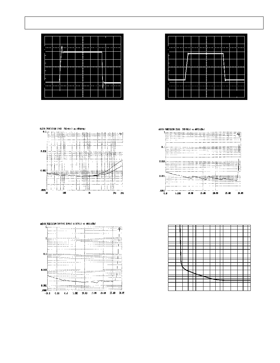
10
90
100
0%
50mV
1
µ
s
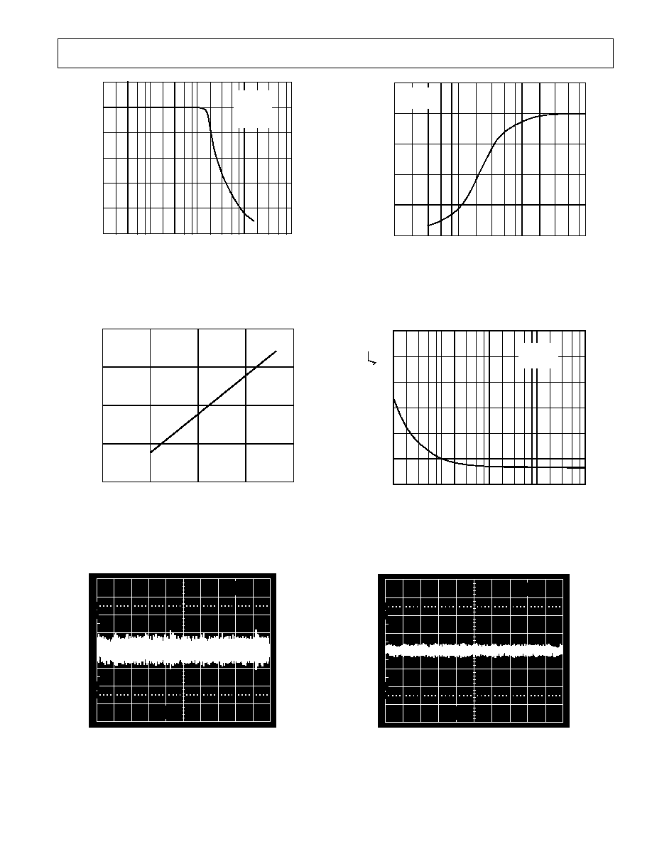
Figure 1. Small-Signal Transient Response (V
IN
=
±
200 mV,
G = 1/2, R
L
= 2 k
, V
S
=
±
15 V, T
A
= +25
°
C)
Figure 3. THD+N vs. Frequency (V
S
=
±
15 V,
V
IN
= 10 V rms, with 80 kHz Filter)
Figure 5. Dynamic Intermodulation Distortion, DIM-100
(V
S
=
±
15 V, R
L
= 100 k
)
10
90
100
0%
5V
5
µ
s
Figure 2. Large Signal Transient Response (V
IN
= +24 dBu,
G = 1/2, R
L
= 2 k
V
S
=
±
15 V, T
A
= +25
°
C)
Figure 4. Headroom (V
S
=
±
15 V, R
L
= 10 k
,
with 80 kHz Filter)
LOAD RESISTANCE
100
10k
1k
100k
1.0
0.0001
0.1
0.001
0.01
THD+N %
Figure 6. THD+N vs. Load (V
S
=
±
15 V, V
IN
= 10 V rms, with
1 kHz Sine, 80 kHz Filter)
SSM2143
REV. 0
4
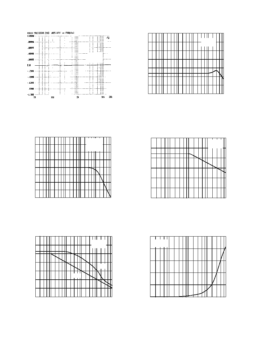
CLOSED-LOOP GAIN dB
V
S
= ±15V
T
A
= +25°C
FREQUENCY Hz
10M
1k
100
100k
10k
1M
40
0
30
30
10
20
20
10
Figure 8. Closed-Loop Gain vs. Frequency, 100 Hz to
10 MHz
1M
1k
100
100k
10k
FREQUENCY Hz
T
A
= +25°C
V
S
= ±15V
120
0
60
20
40
100
80
COMMON-MODE REJECTION dB
Figure 10. Common-Mode Rejection vs. Frequency
1M
1k
100
100k
10k
FREQUENCY Hz
0
T
A
= +25°C
V
S
= ±15V
OUTPUT IMPEDANCE
2
10
6
4
8
Figure 12. Closed-Loop Output Impedance vs. Frequency
Figure 7. Closed-Loop Gain vs. Frequency, 20 Hz to 20 kHz
(Gain of 1/2 Normalized to 0 dB)
180
180
90
135
0
45
45
90
135
PHASE Degrees
FREQUENCY Hz
1k
100
100k
10k
1M
10M
T
A
= +25°C
R
L
= 2k
V
S
= ±15V
Figure 9. Closed-Loop Phase vs. Frequency
140
0
60
20
40
120
80
100
POWER SUPPLY REJECTION dB
FREQUENCY Hz
10
100
1M
100k
1k
10k
PSRR
+PSRR
T
A
= +25°C
V
S
= ±15V
Figure 11. Power Supply Rejection vs. Frequency
V
S
=
±
15V
T
A
= +25
°
C
SSM2143
REV. 0
5
*The photographs in Figure 17 through Figure 19 were taken at V
S
=
±
15 V and T
A
= +25
°
C, using an external amplifier with a gain of 1000.
FREQUENCY Hz
1k
100k
10k
1M
10M
V
S
= ±15V
T
A
= +25°C
R
L
= 2k
G = 1/2
6
0
3
1
2
5
4
OUTPUT VOLTAGE SWING V rms
Figure 13. Output Voltage Swing vs. Frequency
T = +25
°
C
A
SUPPLY VOLTAGE
0
±
20
±
5
±
15
±
10
40
0
30
10
20
OUTPUT VOLTAGE SWING V pp
Figure 15. Output Voltage Swing vs. Supply Voltage
10
90
100
0%
5mV
1s
0.5
µ
V
0V
0.5
µ
V
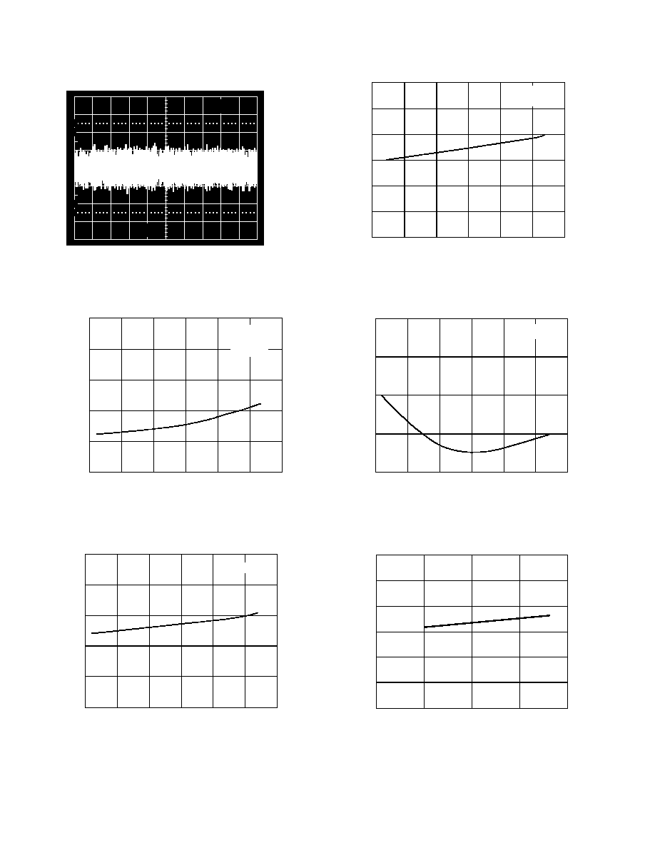
Figure 17. Low Frequency Voltage Noise from 0.1 Hz
to 10 Hz*
LOAD RESISTANCE
10
1k
100
10k
OUTPUT VOLTAGE SWING V rms
0V
7.5V
2.5V
12.5V
5.0V
10.0V
V =
±
15V
T = +25
°
C
S
A
Figure 14. Output Voltage Swing vs. Load Resistance
T
A
= +25°C
V
S
= ±15V
FREQUENCY Hz
1
100
10
1k
10k
120
0
60
20
40
100
80
VOLTAGE NOISE DENSITY nV/ Hz
Figure 16. Voltage Noise Density vs. Frequency
10
90
100
0%
5mV
10ms
5
µ
V
0V
5
µ
V
Figure 18. Voltage Noise from 0 kHz to 1 kHz*
SSM2143
REV. 0
6
*The photographs in Figure 17 through Figure 19 were taken at V
S
=
±
15 V and T
A
= +25
°
C, using an external amplifier with a gain of 1000.
SLEW RATE V/
µ
s
4
16
10
6
8
14
12
TEMPERATURE
°
C
75
25
50
50
25
100
0
R = 2k
V =
±
15V
L
S
Figure 20. Slew Rate vs. Temperature
TEMPERATURE
°
C
75
25
50
50
25
100
0
INPUT OFFSET VOLTAGE
µ
V
400
0
300
100
200
V =
±
15V
S
Figure 22. Input Offset Voltage vs. Temperature
SUPPLY VOLTAGE V
0
±20
±5
±15
±10
SUPPLY CURRENT mA
4.0
1.0
2.5
1.5
2.0
3.5
3.0
T
A
= +25°C
Figure 24. Supply Current vs. Supply Voltage
10
90
100
0%
5mV
1ms
5
µ
V
0V
5
µ
V
Figure 19. Voltage Noise from 0 kHz to 10 kHz*
TEMPERATURE
°
C
75
25
50
50
25
100
0
GAIN ERROR %
0.10
0
0.06
0.02
0.04
0.08
V =
±
10V
V =
±
15V
R = 0
S
S
IN
Figure 21. Gain Error vs. Temperature
TEMPERATURE
°
C
75
25
50
50
25
100
0
V =
±
15V
S
5
0
3
1
2
4
SUPPLY CURRENT mA
Figure 23. Supply Current vs. Temperature
SSM2143
REV. 0
7
APPLICATIONS INFORMATION
The SSM2143 is designed as a balanced differential line re-
ceiver. It uses a high speed, low noise audio amplifier with four
precision thin-film resistors to maintain excellent common-mode
rejection and ultralow THD. Figure 25 shows the basic differen-
tial receiver application where the SSM2143 yields a gain of 1/2.
The placement of the input and feedback resistors can be
switched to achieve a gain of +2, as shown in Figure 26. For
either circuit configuration, the SSM2143 can also be used un-
balanced by grounding one of the inputs. In applications requir-
ing a gain of +1, use the SSM2141.
6
3
5
1
4
2
7
6k
6k
12k
12k
IN
+IN
15V
0.1µF
+15V
0.1µF
A = 2
V
SSM2143
V
OUT
6
1
2
4
5
7
12k
12k
6k
6k
IN
+IN
15V
0.1µF
V
OUT
+15V
0.1µF
A =
V
1
2
SSM2143
3
+
Figure 25. Standard Config-
uration for Gain of 1/2
CMRR
The internal thin-film resistors are precisely trimmed to achieve
a CMRR of 90 dB. Any imbalances introduced by the external
circuitry will cause a significant reduction in the overall CMRR
performance. For example, a 5
source imbalance will result in
a CMRR of 71 dB at dc. This is also true for any reactive source
impedances that may affect the CMRR over the audio frequency
range. These error sources need to be minimized to maintain
the excellent CMRR.
To quantify the required accuracy of the thin film resistor
matching, the source of CMRR error can be analyzed. A resistor
mismatch can be modelled as shown in Figure 27. By assuming
a tolerance on one of the 12 k
resistors of
R, the equation for
the common-mode gain becomes:
V
OUT
V
IN
=
6k
6k
+
12k
6k
12k
+
R
+
1
6k
12k
+
R
which reduces to:
V
OUT
V
IN
=
1/3
R
12k
+
R
This gain error leads to a common-mode rejection ratio of:
CMRR
=
|A
DM
|
|A
CM
|
18k
R
IN
+IN
6k
6k
12k +
R
12k
V
OUT
CMRR =
18k
R
Figure 27. A Small Mismatch in Resistance Results in a
Large Common-Mode Error
Setting
R to 5
results in the CMRR of 71 dB, as stated
above. To achieve the SSM2143's CMRR of 90 dB, the resistor
mismatch can be at most 0.57
. In other words, to build this
circuit discretely, the resistors would have to be matched to
better than 0.005%!
The following table shows typical resistor accuracies and the
resulting CMRR for a differential amplifier.
% Mismatch
CMRR
5%
30 dB
1%
44 dB
0.1%
64 dB
0.005%
90 dB
DC OUTPUT LEVEL ADJUST
The reference node of the SSM2143 is normally connected to
ground. However, it can be used to null out any dc offsets in
the system or to introduce a dc reference level other than
ground. As shown in Figure 28, the reference node needs to be
REFERENCE
OP27
+10V
10V
6
1
2
3
4
5
7
12k
12k
6k
6k
IN
+IN
15V
0.1µF
V
OUT
+15V
0.1µF
SSM2143
Figure 28. A Low Impedance Buffer Is Required to Adjust
the Reference Voltage.
buffered with an op amp to maintain very low impedance to
achieve high CMRR. The same reasoning as above applies such
that the 6 k
resistor has to be matched to better than 0.005%
or 0.3
. The op amp maintains very low output impedance
over the entire audio frequency range, as long as its bandwidth
is well above 20 kHz. The reference input can be adjusted over
a
±
10 V range. The gain from the reference to the output is
unity so the resulting dc output adjustment range is also
±
10 V.
INPUT ERRORS
The main dc input offset error specified for the SSM2143 is the
Input Offset Voltage. The Input Bias Current and Input Offset
Current are not specified as for a normal operational amplifier.
Because the SSM2143 has built-in resistors, any bias current
related errors are converted into offset voltage errors. Thus, the
offset voltage specification is a combination of the amplifier's
offset voltage plus its offset current times the input impedance.
Figure 26. Reversing the
Resistors Results in a
Gain of 2
Figure 29. SSM2142/SSM2143 Balanced Line Driver/
Receiver System
2
6
5
4
3
8
7
SSM2142
V
IN
SSM2143
+18V
18V
+18V
0.1µF
0.1µF
18V
V
OUT
3
7
6
4
1
2
5
ALL CABLE MEASUREMENTS USE
BELDEN CABLE (500').
1
SSM2143
REV. 0
8
C15982411/91
LINE DRIVER/RECEIVER SYSTEM
The SSM2143 and SSM2142 provide a fully integrated line driver/
receiver system. The SSM2142 is a high performance balanced
line driver IC that converts an unbalanced input into a balanced
output signal. It can drive large capacitive loads on long cables
making it ideal for transmitting balanced audio signals. When com-
bined with an SSM2143 on the receiving end of the cable, the sys-
tem maintains high common-mode rejection and ultralow THD.
The SSM2142 is designed with a gain of +2 and the SSM2143
with a gain of 1/2, providing an overall system gain of unity.
The following data demonstrates the typical performance of the
two parts together, measured on an Audio Precision at the
SSM2143's output. This configuration was tested with 500 feet
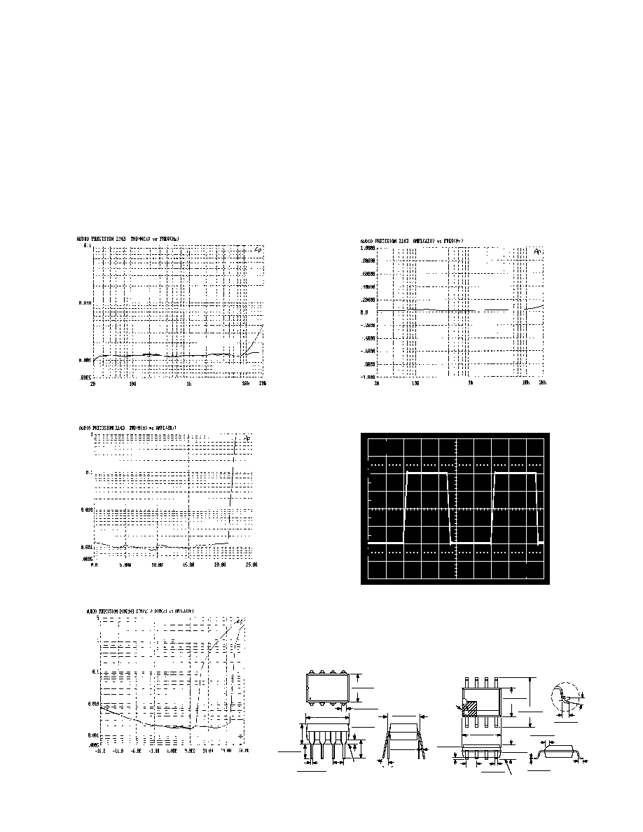
Figure 30. THD+N vs. Frequency of SSM2142/SSM2143
System (V
S
=
±
18 V, V
IN
= 5 V rms, with 80 kHz Filter)
Figure 31. SSM2142/SSM2143 System Headroom
See Text--(V
S
=
±
18 V, R
L
= 10 k
, 500' Cable)
Figure 32. SSM2142/SSM2143 System
DIM-100 Dynamic Intermodulation
Distortion (V
S
=
±
18 V, R
L
= 10 k
)
of cable between the ICs as well as no cable. The combination
of the two parts results in excellent THD+N and SNR and a noise
floor of typically 105 dB over a 20 Hz to 20 kHz bandwidth.
A comment on SSM2142/SSM2143 system headroom is neces-
sary. Figure 31 shows a maximum signal handling of approximately
±
22 dBu, but it must be kept in mind that this is measured be-
tween the SSM2142's input and SSM2143's output, which has
been attenuated by one half. Normally, the system would be shown
as actually used in a piece of equipment, whereby the SSM2143 is
at the input and SSM2142 at the output. In this case, the system
could handle differential signals in excess of +24 dBu at the input
and output, which is consistent with headroom requirements of
most professional audio equipment.
Figure 33. SSM2142/SSM2143 System Frequency
Response (V
S
=
±
18 V, V
IN
= 0 dBV, 500' Cable)
10
90
100
0%
5V
10
µ
s
Figure 34. SSM2142/SSM2143 System Large Signal Pulse
Response (V
S
=
±
18 V, R
L
= 10 k
, No Cable)
OUTLINE DIMENSIONS
Dimensions shown in inches and (mm).
PRINTED IN U.S.A.
500' CABLE
NO CABLE
500' CABLE
NO CABLE
N-8
0.200 (5.05)
0.125 (3.18)
0.150
(3.81)
MIN
0.210
(5.33)
MAX
0.430 (10.92)
0.348 (8.84)
0.280 (7.11)
0.240 (6.10)
4
5
8
1
0.070 (1.77)
0.045 (1.15)
0.022 (0.558)
0.014 (0.356)
0.325 (8.25)
0.300 (7.62)
0 - 15
0.100
(2.54)
BSC
0.015 (0.381)
0.008 (0.204)
SEATING
PLANE
0.060 (1.52)
0.015 (0.38)
SO-8
SEATING
PLANE
SEE DETAIL
ABOVE
4
5
8
1
0.0688 (1.75)
0.0532 (1.35)
0.0098 (0.25)
0.0075 (0.19)
0.1574 (4.00)
0.1497 (3.80)
0.2440 (6.20)
0.2284 (5.80)
0.1968 (5.00)
0.1890 (4.80)
0.0192 (0.49)
0.0138 (0.35)
0.0500
(1.27)
BSC
0.0098 (0.25)
0.0040 (0.10)
×
45
°
0.0196 (0.50)
0.0099 (0.25)
0.0500 (1.27)
0.0160 (0.41)
PIN 1
0
°
- 8
°