 | ÐлекÑÑоннÑй компоненÑ: SSM2164P | СкаÑаÑÑ:  PDF PDF  ZIP ZIP |
Äîêóìåíòàöèÿ è îïèñàíèÿ www.docs.chipfind.ru
One Technology Way, P.O. Box 9106, Norwood. MA 02062-9106, U.S.A.
Tel: 617/329-4700
Fax: 617/326-8703
REV. 0
Information furnished by Analog Devices is believed to be accurate and
reliable. However, no responsibility is assumed by Analog Devices for its
use, nor for any infringements of patents or other rights of third parties
which may result from its use. No license is granted by implication or
otherwise under any patent or patent rights of Analog Devices.
a
Low Cost Quad
Voltage Controlled Amplifier
SSM2164
GENERAL DESCRIPTION
The SSM2164 contains four independent voltage controlled
amplifiers (VCAs) in a single package. High performance
(100 dB dynamic range, 0.02% THD) is provided at a very low
cost-per-VCA, resulting in excellent value for cost sensitive gain
control applications. Each VCA offers current input and output
for maximum design flexibility, and a ground referenced
33 mV/dB control port.
All channels are closely matched to within 0.07 dB at unity gain,
and 0.24 dB at 40 dB of attenuation. A 120 dB gain range is
possible.
A single resistor tailors operation between full Class A and AB
modes. The pinout allows upgrading of SSM2024 designs with
minimal additional circuitry.
The SSM2164 will operate over a wide supply voltage range of
±
4 V to
±
18 V. Available in 16-pin P-DIP and SOIC packages,
the device is guaranteed for operation over the extended
industrial temperature range of 40
°
C to +85
°
C.
FEATURES
Four High Performance VCAs in a Single Package
0.02% THD
No External Trimming
120 dB Gain Range
0.07 dB Gain Matching (Unity Gain)
Class A or AB Operation
APPLICATIONS
Remote, Automatic, or Computer Volume Controls
Automotive Volume/Balance/Faders
Audio Mixers
Compressor/Limiters/Compandors
Noise Reduction Systems
Automatic Gain Controls
Voltage Controlled Filters
Spatial Sound Processors
Effects Processors
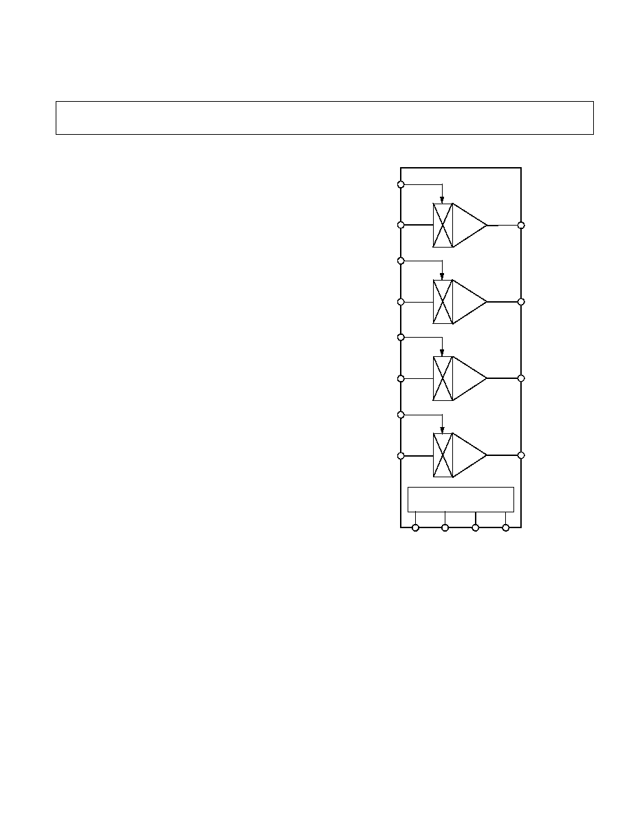
FUNCTIONAL BLOCK DIAGRAM
POWER SUPPLY
AND BIASING CIRCUITRY
VCA4
VCA3
VCA2
VCA1
V+
GND
V
MODE
I
IOUT
I
IOUT
I
IOUT
I
IOUT
V
C
V
C
V
C
V
C
I
IN
I
IN
I
IN
I
IN
SSM2164SPECIFICATIONS
ELECTRICAL SPECIFICATIONS
SSM2164
Parameter
Conditions
Min
Typ
Max
Units
AUDIO SIGNAL PATH
Noise
V
IN
= GND, 20 kHz Bandwidth
94
dBu
Headroom
Clip Point = 1% THD+N
22
dBu
Total Harmonic Distortion
2nd and 3rd Harmonics Only
A
V
= 0 dB, Class A
0.02
.1
%
A
V
=
±
20 dB, Class A
1
0.15
%
A
V
= 0 dB, Class AB
0.16
%
A
V
=
±
20 dB, Class AB
1
0.3
%
Channel Separation
110
dB
Unity Gain Bandwidth
C
F
= 10 pF
500
kHz
Slew Rate
C
F
= 10 pF
0.7
mA/
µ
s
Input Bias Current
±
10
nA
Output Offset Current
V
IN
= 0
±
50
nA
Output Compliance
±
0.1
V
CONTROL PORT
Input Impedance
5
k
Gain Constant
(Note 2)
33
mV/dB
Gain Constant Temperature Coefficient
3300
ppm/
°
C
Control Feedthrough
0 dB to 40 dB Gain Range
3
1.5
8.5
mV
Gain Matching, Channel-to-Channel
A
V
= 0 dB
0.07
dB
A
V
= 40 dB
0.24
dB
Maximum Attenuation
100
dB
Maximum Gain
+20
dB
POWER SUPPLIES
Supply Voltage Range
±
4
±
18
V
Supply Current
Class AB
6
8
mA
Power Supply Rejection Ratio
60 Hz
90
dB
NOTES
1
10 dBu input @ 20 dB gain; +10 dBu input @ 20 dB gain.
2
After 60 seconds operation.
3
+25
°
C to +85
°
C.
Specifications subject to change without notice.
REV. 0
2
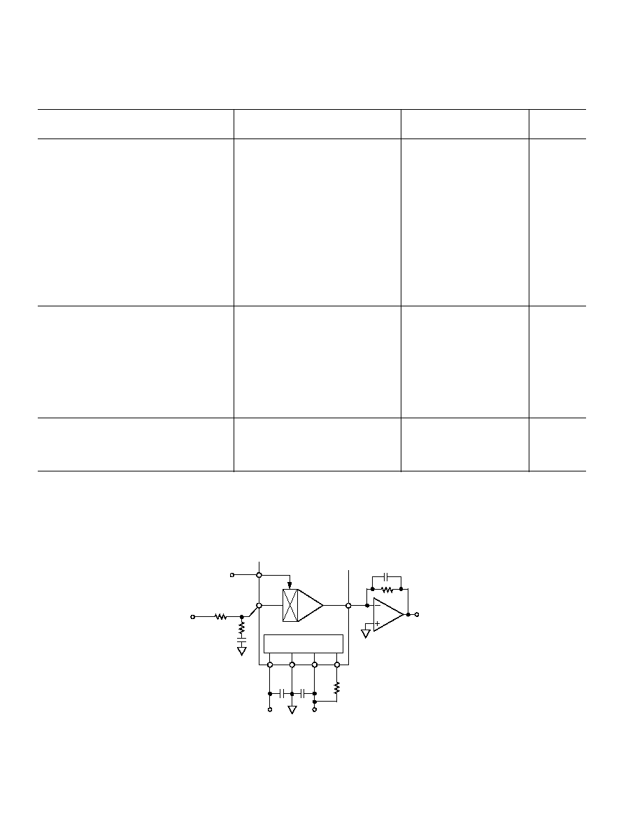
TYPICAL APPLICATION AND TEST CIRCUIT
(V
S
=
±
15 V, A
V
= 0 dB, 0 dBu = 0.775 V
rms, V
IN
= 0 dBu, R
IN
= R
OUT
= 30 k
, f = 1 kHz,
40
°
C < T
A
< +85
°
C using Typical Application Circuit (Class AB), unless otherwise noted. Typical specifications apply at T
A
= +25
°
C.)
30k
V
IN4
500
560pF
POWER SUPPLY
AND BIASING CIRCUITRY
VCA4
9
8
16
1
V
GND
V+
MODE
0.1µF
0.1µF
R
B
(7.5k
CLASS A)
(OPEN CLASS AB)
+15V
15V
1/2
OP275
30k
100pF
V
OUT4
I
IOUT
13
14
15
V
C4
I
IN
V
C
Figure 1. R
IN
= R
OUT
= 30 k
, C
F
= 100 pF. Optional R
B
= 7.5 k
, Biases Gain Core to Class A Opera-
tion. For Class AB, Omit R
B
.
SSM2164
REV. 0
3
ORDERING GUIDE
Temperature
Package
Package
Model
Range
Description
Options
SSM2164P
40
°
C to +85
°
C
Plastic DIP
N-16
SSM2164S
40
°
C to +85
°
C
Narrow SOIC
R-16A
ABSOLUTE MAXIMUM RATINGS
Supply Voltage . . . . . . . . . . . . . . . . . . . . . . . . . . . . . . . .
±
18 V
Input, Output, Control Voltages . . . . . . . . . . . . . . . . V to V+
Output Short Circuit Duration to GND . . . . . . . . . Indefinite
Storage Temperature Range . . . . . . . . . . . . 65
°
C to +150
°
C
Operating Temperature Range . . . . . . . . . . . . . 40
°
C to +85
°
C
Junction Temperature Range . . . . . . . . . . . . 65
°
C to +150
°
C
Lead Temperature Range (Soldering 60 sec) . . . . . . . . +300
°
C
Package Type
JA
*
JC
Units
16-Pin Plastic DIP (P Suffix)
76
33
°
C/W
16-Pin SOIC (S Suffix)
92
27
°
C/W
*
JA
is specified for the worst case conditions; i.e.,
JA
is specified for device in socket
for P-DIP packages,
JA
is specified for device soldered in circuit board for SOIC
package.
PIN CONFIGURATION
16-Lead Epoxy DIP and SOIC
MODE
I
IN1
V+
I
IN4
I
OUT2
V
C2
I
IN2
I
OUT3
V
C3
I
IN3
V
C1
I
OUT1
V
C4
I
OUT4
GND
V
1
2
16
15
5
6
7
12
11
10
3
4
14
13
8
9
TOP VIEW
(Not to Scale)
SSM2164
WARNING!
ESD SENSITIVE DEVICE
CAUTION
ESD (electrostatic discharge) sensitive device. Electrostatic charges as high as 4000 V readily
accumulate on the human body and test equipment and can discharge without detection.
Although the SSM2164 features proprietary ESD protection circuitry, permanent damage may
occur on devices subjected to high energy electrostatic discharges. Therefore, proper ESD
precautions are recommended to avoid performance degradation or loss of functionality.
SSM2164
REV. 0
4
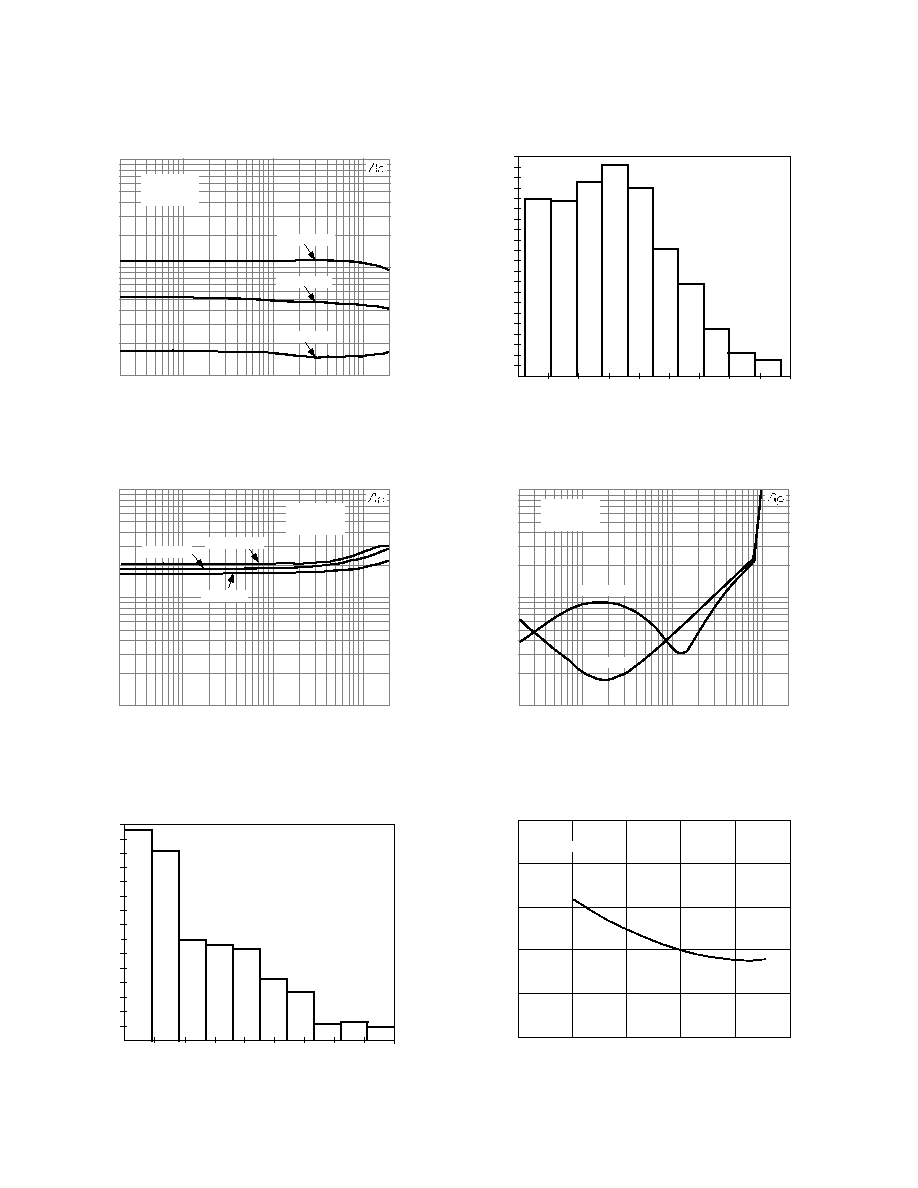
Typical Performance Characteristics
Figure 2. THD+N vs. Frequency, Class A
Figure 3. THD+N vs. Frequency Class, AB
Figure 4. THD Distribution, Class A
300
280
260
240
200
180
160
140
120
100
60
40
20
0
80
220
0.005 0.010
0.015
0.020 0.025
0.030
0.035 0.040
0.045
0.050
THD %
UNITS
V
S
=
±
15V
T
A
= +25
°
C
1200 CHANNELS
Figure 5. THD Distribution, Class AB
210
200
190
180
170
160
150
140
130
120
110
100
90
80
70
60
50
40
30
20
10
0
UNITS
0.00
0.05
0.10
0.15
0.20
0.25
0.30
0.35
0.40
0.45
THD %
V
S
=
±
15V
T
A
= +25
°
C
1200 CHANNELS
Figure 6. THD+N vs. Amplitude
Figure 7. THD+N vs. Supply Voltage, Class A
0.10
0
±
20
0.06
0.02
±
4
0.04
0
0.08
±
16
±
12
±
8
THD + N %
SUPPLY Volts
LPF = 80kHz
1.0
0.1
0.01
THD + N %
20
100
1k
10k
20k
FREQUENCY Hz
CLASS A
V
S
=
±
15V
LPF = 80kHz
A
V
= + 20dB
A
V
= 20dB
A
V
= 0dB
1.0
0.1
0.01
THD + N %
20
100
1k
10k
20k
FREQUENCY Hz
A
V
= 20dB
A
V
= +20dB
A
V
= 0dB
CLASS AB
V
S
=
±
15V
LPF = 80kHz
AMPLITUDE V
RMS
1.0
0.1
0.01
THD + N %
20
100
1k
10k
20k
V
S
±
15V
A
V
= 0dB
LPF = 22kHz
CLASS A
CLASS AB
SSM2164
REV. 0
5
Figure 11. Voltage Noise Density vs. R
BIAS
Figure 8. THD vs. Temperature, Class A
Figure 9. THD vs. Temperature, Class AB
Figure 12. THD vs. R
BIAS
Figure 13. Control Feedthrough vs. R
BIAS
Figure 10. Voltage Noise Density vs. Frequency, Class AB
1000
100
10
1k
10k
1M
100k
R
BIAS
VOLTAGE NOISE DENSITY nV/ Hz
V
S
=
±
15V
T
A
= +25
°
C
1.0
0.1
0.01
1k
10k
1M
100k
R
BIAS
V
S
=
±
15V
T
A
= +25
°
C
THD %
0.030
0.025
0.020
0.015
0.010
40
20
0
20
40
60
80
TEMPERATURE
°
C
% THD
V
S
=
±
15V
V
IN
= 0dBu
A
V
= 0dB
500
400
0
1
10
100k
10k
1k
100
300
200
100
FREQUENCY Hz
V
S
=
±
15V
R
IN
= R
F
= 30k
T
A
= +25
°
C
NOISE nV/ Hz
0.30
0.25
0.20
0.15
0.10
40
20
0
20
40
60
80
TEMPERATURE
°
C
% THD
V
S
=
±
15V
V
IN
= 0dBu
A
V
= 0dB
1k
10k
1M
100k
R
BIAS
10
5
20
10
15
0
5
CONTROL FEEDTHROUGH mV
V
S
=
±
15V
T
A
= +25
°
C
SSM2164
REV. 0
6
Typical Performance Characteristics
15
0
15
10k
10M
1M
100k
1k
V
S
=
±
15V
T
A
= +25
°
C
A
V
= 0dB
C
F
= 10pF
PHASE
GAIN
5
10
5
10
0
90
180
90
180
GAIN dB
FREQUENCY Hz
PHASE Degrees
Figure 14. Gain/Phase vs. Frequency
0.1
0.1
0.4
100
100k
10k
1k
10
0.2
0.3
0
GAIN dB
FREQUENCY Hz
C
F
= 100pF
C
F
= 10pF
V
S
=
±
15V
T
A
= +25
°
C
A
V
= 0dB
Figure 15. Gain Flatness vs. Frequency
40
20
60
100
1k
10M
1M
100k
10k
0
20
40
FREQUENCY Hz
GAIN dB
A
V
= +20dB
A
V
= 0dB
A
V
= 20dB
V
S
=
±
15V
T
A
= +25
°
C
C
F
= 10pF
Figure 16. Bandwidth vs. Gain
Figure 17. 3 dB Bandwidth vs. I-to-V Feedback Capacitor
30
15
0
1
10
100
5
10
20
25
SLEW RATE V/
µ
s
I TO V FEEDBACK CAPACITOR pF
±
SLEW RATE
V
S
=
±
15V
T
A
= +25
°
C
OP275 OUTPUT
AMPLIFIER
Figure 18. Slew Rate vs. I-to-V Feedback Capacitor
20
20
80
1k
1M
100k
10k
100
40
60
0
FREQUENCY Hz
V
S
=
±
15V
T
A
= +25
°
C
V
IN
= 0V
R
F
= R
IN
= 30k
CONTROL FEEDTHROUGH dB
Figure 19. Control Feedthrough vs. Frequency
10M
1M
10k
1
10
1000
100
100k
3dB BANDWIDTH Hz
I TO V FEEDBACK CAPACITOR pF
V
S
=
±
15V
T
A
= +25
°
C
SSM2164
REV. 0
7
0
20
100
10
100
1M
100K
10k
1k
40
60
80
FREQUENCY Hz
PSRR dB
V
S
=
±
15V
T
A
= +25
°
C
+PSRR
PSRR
Figure 20. PSRR vs. Frequency
25
20
0
1k
10k
1M
100k
15
10
5
SUPPLY CURRENT mA
R
BIAS
+ISY
ISY
V
S
=
±
15V
T
A
= +25
°
C
Figure 21. Supply Current vs. R
BIAS
45
20
100
35
25
25
30
50
40
75
50
25
0
GAIN CONSTANT mV/dB
TEMPERATURE
°
C
CLASS A AND
CLASS AB
V
S
=
±
15V
Figure 22. Gain Constant vs. Temperature
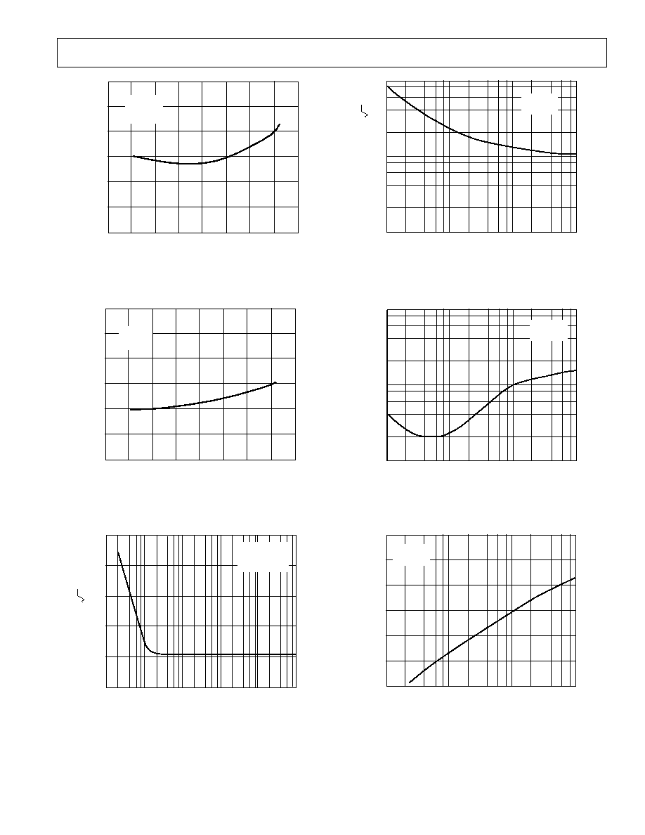
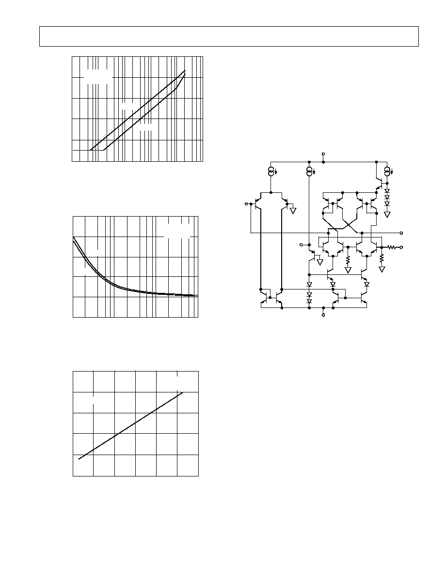
APPLICATIONS INFORMATION
Circuit Description
The SSM2164 is a quad Voltage Controlled Amplifier (VCA)
with 120 dB of gain control range. Each VCA is a current-in,
current-out device with a separate 33 mV/dB voltage input
control port. The class of operation (either Class A or Class
AB) is set by a single external resistor allowing optimization of
the distortion versus noise tradeoff for a particular application.
The four independent VCAs in a single 16-pin package make
the SSM2164 ideal for applications where multiple volume
control elements are needed.
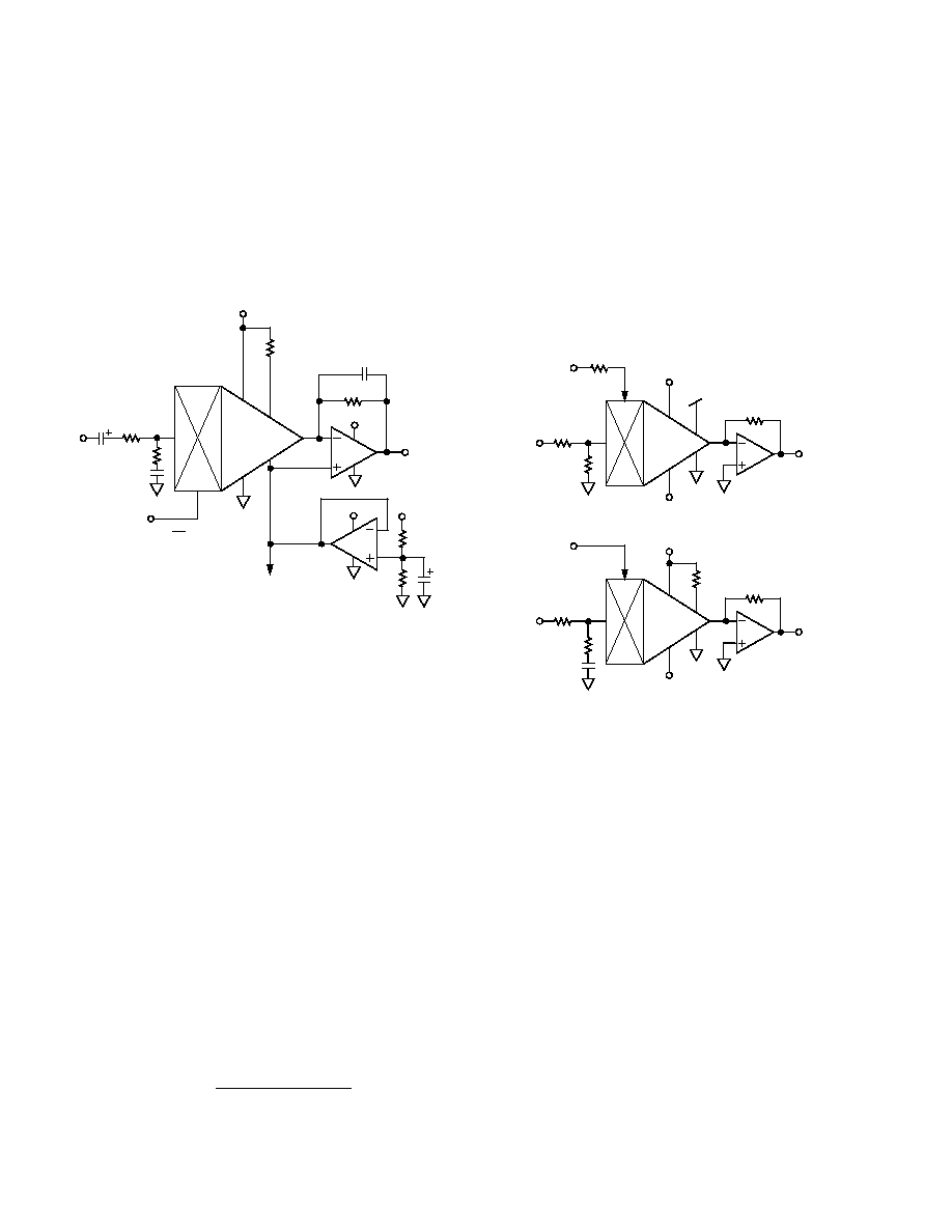
Figure 23. Simplified Schematic (One Channel)
The simplified schematic in Figure 23 shows the basic structure
of one of the four VCAs in the device. The gain core is com-
prised of the matched differential pairs Q1-Q4 and the current
mirrors of Q5, Q6 and Q7, Q8. The current input pin, I
IN
, is
connected to the collectors of Q1 and Q7, and the difference in
current between these two transistors is equivalent to I
IN
. For
example, if 100
µ
A is flowing into the input, Q1's collector
current will be 100
µ
A higher than Q7's collector current.
Varying the control voltage V
C
, steers the signal current from
one side of each differential pair to the other, resulting in either
gain or attenuation. For example, a positive voltage on V
C
steers more current through Q1 and Q4 and decreases the
current in Q2 and Q3. The current output pin, I
OUT
, is con-
nected to the collector of Q3 and the current mirror (Q6) from
Q2. With less current flowing through these two transistors, less
current is available at the output. Thus, a positive V
C
attenuates
the input and a negative V
C
amplifies the input. The VCA has
unity gain for a control voltage of 0.0 V where the signal current
is divided equally between the gain core differential pairs.
The MODE pin allows the setting of the quiescent current in
the gain core of the VCA to trade off the SSM2164's THD and
noise performance to an optimal level for a particular applica-
tion. Higher current through the core results in lower distortion
Q6
Q5
Q8
Q7
Q2
Q1
Q4
Q3
I
IN
I
OUT
V
C
4.5k
500
450
MODE
V
V+
SSM2164
REV. 0
8
but higher noise, and the opposite is true for less current. The
increased noise is due to higher current noise in the gain core
transistors as their operating current is increased. THD has the
opposite relationship to collector current. The lower distortion
is due to the decrease in the gain core transistors' emitter
impedance as their operating current increases.
This classical tradeoff between THD and noise in VCAs is
usually expressed as the choice of using a VCA in either Class A
or Class AB mode. Class AB operation refers to running a VCA
with less current in the gain core, resulting in lower noise but
higher distortion. More current in the core corresponds to
Class A performance with its lower THD but higher noise.
Figures 11 and 12 show the THD and noise performance of the
SSM2164 as the bias current is adjusted. Notice the two
characteristics have an inverse characteristic.
The quiescent current in the core is set by adding a single
resistor from the positive supply to the MODE pin. As the
simplified schematic shows, the potential at the MODE pin is
one diode drop above the ground pin. Thus, the formula for the
MODE current is:
I
MODE
=
(V
+
)
-
0.6V
R
B
With
±
15 V supplies, an R
B
of 7.5k gives Class A biasing with a
current of 1.9 mA. Leaving the MODE pin open sets the
SSM2164 in Class AB with 30
µ
A of current in the gain core.
Basic VCA Configuration
Figure 24 shows the basic application circuit for the SSM2164.
Each of the four channels is configured identically. A 30 k
resistor converts the input voltage to an input current for the
VCA. Additionally, a 500
resistor in series with a 560 pF
capacitor must be added from each input to ground to ensure
stable operation. The output current pin should be maintained
at a virtual ground using an external amplifier. In this case the
OP482 quad JFET input amplifier is used. Its high slew rate,
wide bandwidth, and low power make it an excellent choice for
the current-to-voltage converter stage. A 30 k
feedback
resistor is chosen to match the input resistor, giving unity gain
for a 0.0 V control voltage. The 100 pF capacitors ensure
stability and reduce high frequency noise. They can be
increased to reduce the low pass cutoff frequency for further
noise reduction.
For this example, the control voltage is developed using a
100 k
potentiometer connected between +5 V and ground.
This configuration results in attenuation only. To produce both
gain and attenuation, the potentiometer should be connected
between a positive and negative voltage. The control input has
an impedance of 5 k
. Because of this, any resistance in series
with V
C
will attenuate the control signal. If precise control of
the gain and attenuation is required, a buffered control voltage
should be used.
Notice that a capacitor is connected from the control input to
ground. Because the control port is connected directly to the
gain core transistors, any noise on the V
C
pin will increase the
output noise of the VCA. Filtering the control voltage ensures
that a minimal amount of noise is introduced into the VCA,
allowing its full performance to be realized. In general, the
largest possible capacitor value should be used to set the filter at
a low cutoff frequency. The main exception to this is in
dynamic processing applications, where faster attack or decay
times may be needed.
Figure 24. Basic Quad VCA Configuration
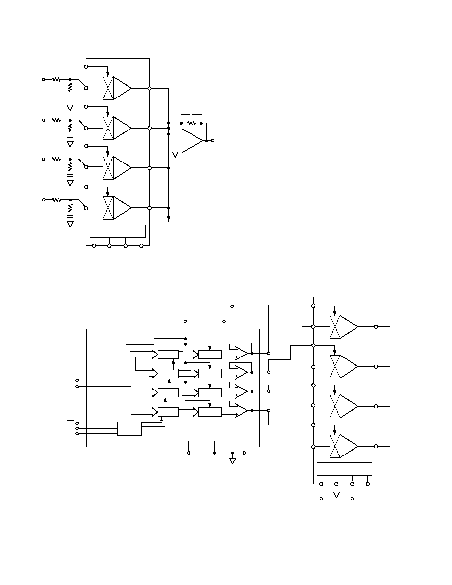
Low Cost, Four-Channel Mixer
The four VCAs in a single package can be configured to create a
simple four-channel mixer as shown in Figure 25. The inputs
and control ports are configured the same as for the basic VCA,
but the outputs are summed into a single output amplifier. The
OP176 is an excellent amplifier for audio applications because
of its low noise and distortion and high output current drive.
The amount of signal from each input to the common output
can be independently controlled using up to 20 dB of gain or as
much as 100 dB of attenuation. Additional SSM2164s could be
added to increase the number of mixer channels by simply
summing their outputs into the same output amplifier. Another
possible configuration is to use a dual amplifier such as the
OP275 to create a stereo, two channel mixer with a single
SSM2164.
1µF
1µF
1µF
1µF
+5V
100k
30k
V
IN4
500
560pF
POWER SUPPLY
AND BIASING CIRCUITRY
VCA4
+5V
100k
30k
V
IN3
500
560pF
VCA3
+5V
100k
30k
V
IN2
500
560pF
VCA2
+5V
100k
30k
V
IN1
500
560pF
VCA1
9
8
16
1
V
GND
V+
MODE
0.1µF
0.1µF
R
B
(7.5k
CLASS A)
(OPEN CLASSAB)
+15V
15V
1/4
OP482
1/4
OP482
1/4
OP482
1/4
OP482
30k
30k
30k
30k
100pF
100pF
100pF
100pF
V
OUT1
V
OUT2
V
OUT3
V
OUT4
I
IOUT
I
IOUT
I
IOUT
I
IOUT
3
2
6
7
4
5
13
12
11
10
14
15
V
C
I
IN
I
IN
V
C
I
IN
V
C
I
IN
V
C
SSM2164
REV. 0
9
30k
500
560pF
POWER SUPPLY
AND BIASING CIRCUITRY
VCA4
30k
500
560pF
VCA3
30k
500
560pF
VCA2
30k
500
560pF
VCA1
V+
GND
V
MODE
30k
100pF
V
OUT
I
IOUT
I
IOUT
I
IOUT
I
IOUT
OP176
FROM ADDITIONAL SSM2164s
FOR > 4 CHANNELS
V
C
V
C
V
C
V
C
I
IN
I
IN
I
IN
I
IN
If additional SSM2164s are added, the 100 pF capacitor may
need to be increased to ensure stability of the output amplifier.
Most op amps are sensitive to capacitance on their inverting
inputs. The capacitance forms a pole with the feedback resistor,
which reduces the high frequency phase margin. As more
SSM2164's are added to the mixer circuit, their output capaci-
tance and the parasitic trace capacitance add, increasing the
overall input capacitance. Increasing the feedback capacitor will
maintain the stability of the output amplifier.
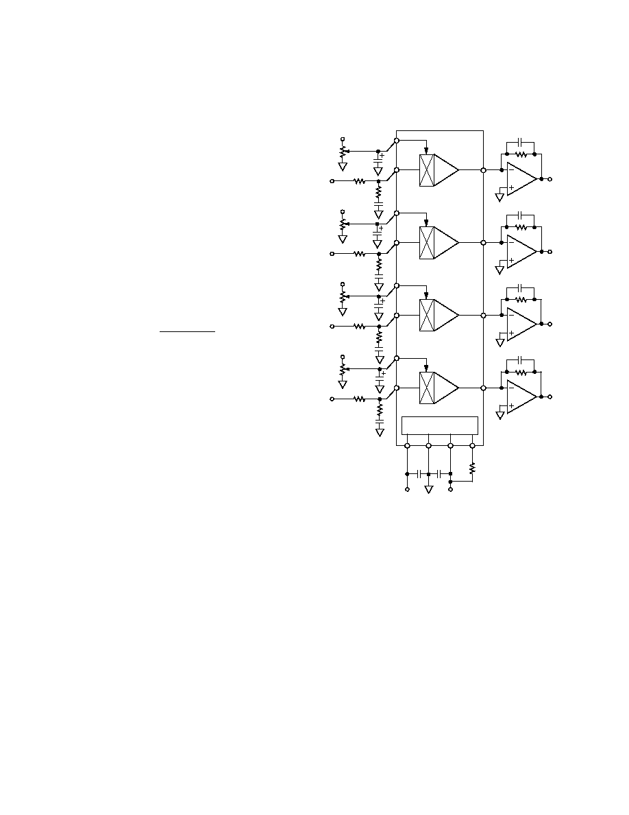
Digital Control of the SSM2164
One option for controlling the gain and attenuation of the
SSM2164 is to use a voltage output digital-to-analog converter
such as the DAC8426 (Figure 26), whose 0 V to +10 V output
controls the SSM2164's attenuation from 0 dB to 100 dB. Its
simple 8-bit parallel interface can easily be connected to a
microcontroller or microprocessor in any digitally controlled
system. The voltage output configuration of the DAC8426
provides a low impedance drive to the SSM2164 so the attenua-
tion can be controlled accurately. The 8-bit resolution of the
DAC and its full-scale voltage of +10 V gives an output of
3.9 mV/bit. Since the SSM2164 has a 33 mV/dB gain con-
stant, the overall control law is 0.12 dB/bit or approximately
8 bits/dB. The input and output configuration for the
SSM2164 is the same as for the basic VCA circuit shown
earlier. The 4-to-1 mixer configuration could also be used.
LATCH A
LATCH B
LATCH C
LATCH D
DAC A
DAC B
DAC C
DAC D
LOGIC
CONTROL
10V
REFERENCE
DATA BUS
3
5
6
V
SS
AGND
DGND
15
16
17
WR
A1
A0
14
7
LSB
MSB
4
V
REF
OUT +10V
18
V
DD
+15V
2
1
20
19
V
OUTA
V
OUTB
V
OUTC
V
OUTD
DAC8426
POWER SUPPLY
AND BIASING CIRCUITRY
VCA4
VCA3
VCA2
VCA1
V+
GND
V MODE
I
IOUT
I
IOUT
I
IOUT
I
IOUT
V
C
V
C
V
C
V
C
I
IN
I
IN
I
IN
I
IN
+15V
15V
Figure 26. Digital Control of VCA Gain
Figure 25. Four-Channel Mixer (4 to 1)
SSM2164
REV. 0
10
Single Supply Operation
The SSM2164 can easily be operated from a single power
supply as low as +8 V or as high as +36 V. The key to using a
single supply is to reference all ground connections to a voltage
midway between the supply and ground as shown in Figure 27.
The OP176 is used to create a pseudo-ground reference for the
SSM2164. Both the OP482 and OP176 are single supply
amplifiers and can easily operate over the same voltage range as
the SSM2164 with little or no change in performance.
GND
MODE
V+
V
16
1
9
8
V+ = +8V
R
B
V
C
(0dB GAIN AT V
C
= )
V+
2
500
560pF
30k
10µF
V
IN
V+
1/4
OP482
OP176
V+
30k
V
OUT
10k
10k
V+
10µF
V+/2
TO ADDITIONAL
OP482 AMPLIFIERS
(1.8k
FOR
CLASS A)
(OPEN FOR
CLASS B)
100pF
Figure 27. Single Supply Operation of the SSM2164
(One Channel Shown)
The reference voltage is set by the resistor divider from the
positive supply. Two 10 k
resistors create a voltage equal to
the positive supply divided by 2. The 10
µ
F capacitor filters the
supply voltage, providing a low noise reference to the circuit.
This reference voltage is then connected to the GND pin of the
SSM2164 and the noninverting inputs of all the output amplifi-
ers. It is important to buffer the resistor divider with the OP176
to ensure a low impedance pseudo-ground connection for the
SSM2164.
The input can either be referenced to this same mid-supply
voltage or ac coupled as is done in this case. If the entire system
is single supply, then the input voltage will most likely already
be referenced to the midpoint; if this is the case, the 10
µ
F
input capacitor can be eliminated. Unity gain is set when V
C
equals the voltage on the GND pin. Thus, the control voltage
should also be referenced to the same midsupply voltage.
The value of the MODE setting resistor may also change
depending on the total supply voltage. Because the GND pin is
at a pseudo-ground potential, the equation to set the MODE
current now becomes:
I
MODE
=
(V
+
)
-
V
GND
-
0.6V
R
B
The value of 1.8 k
results in Class A biasing for the case of
using a +8 V supply.
Upgrading SSM2024 Sockets
The SSM2164 is intended to replace the SSM2024, an earlier
generation quad VCA. The improvements in the SSM2164
have resulted in a part that is not a drop-in replacement to the
SSM2024, but upgrading applications with the SSM2024 is a
simple task. The changes are shown in Figure 28. Both parts
have identical pinouts with one small exception. The MODE
input (Pin 1) does not exist on the SSM2024. It has fixed
internal biasing, whereas flexibility was designed into the
SSM2164. A MODE set resistor should be added for Class A
operation, but if the SSM2164 is going to be operated in Class
AB, no external resistor is needed.
V+
16
1
9
8
200
10k
V
IN1
NC
SSM2024
V
10k
V
OUT1
4
V
C1
10k
3
2
V+
16
1
9
8
500
30k
V
IN1
SSM2164
V
30k
V
OUT1
4
V
C1
3
2
560pF
R
B
Figure 28. Upgrading SSM2024 Sockets with SSM2164
Since both parts are current output devices, the output configu-
ration is nearly identical, except that the 10 k
resistors should
be increased to 30 k
to operate the SSM2164 in its optimum
range. The 10 k
input resistor for the SSM2024 should also
be increased to 30 k
to match the output resistor. Addition-
ally, the 200
resistor should be replaced by a 500
resistor in
series with 560 pF for the SSM2164 circuit.
One last change is the control port configuration. The
SSM2024's control input is actually a current input. Thus, a
resistor was needed to change the control voltage to a current.
This resistor should be removed for the SSM2164 to provide a
direct voltage input. In addition, the SSM2024 has a log/log
control relationship in contrast to the SSM2164's linear/log gain
constant. The linear input is actually much easier to control,
but the difference may necessitate adjusting a SSM2024 based
circuit's control voltage gain curve. By making these relatively
simple changes, the superior performance of the SSM2164 can
easily be realized.
SSM2164
REV. 0
11
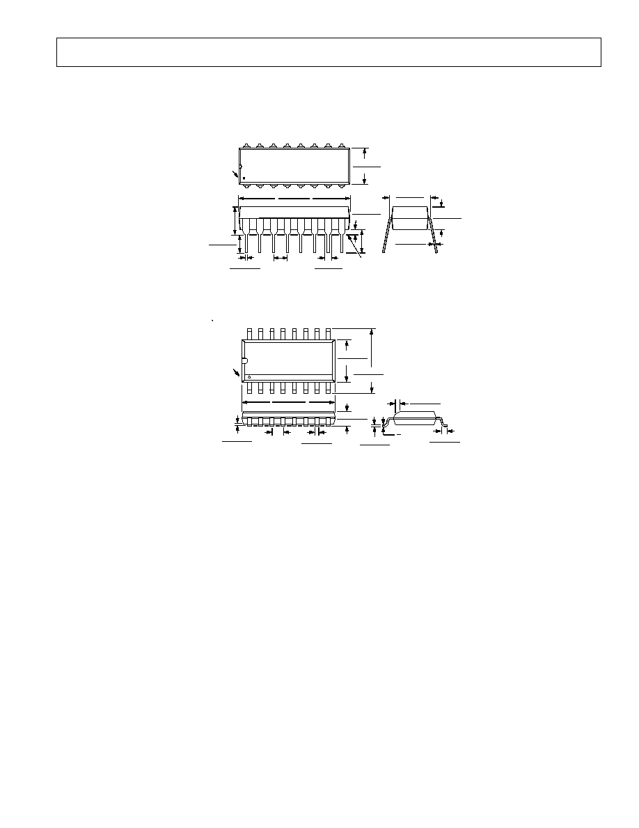
OUTLINE DIMENSIONS
Dimensions shown in inches and (mm).
16-Pin Plastic DIP (N-16)
16-Pin Narrow SOIC (R-16A)
0.210
(5.33)
MAX
0.160 (4.06)
0.115 (2.93)
0.022 (0.558)
0.014 (0.356)
0.100
(2.54)
BSC
PIN 1
0.280 (7.11)
0.240 (6.10)
0.325 (8.25)
0.300 (7.62)
0.015 (0.381)
0.008 (0.204)
0.195 (4.95)
0.115 (2.93)
SEATING
PLANE
0.060 (1.52)
0.015 (0.38)
0.130
(3.30)
MIN
0.070 (1.77)
0.045 (1.15)
0.840 (21.33)
0.745 (18.93)
9
16
1
8
PIN 1
0.1574 (4.00)
0.1497 (3.80)
0.2440 (6.20)
0.2284 (5.80)
1
16
9
8
0.0500 (1.27)
0.0160 (0.41)
8
°
0
°
0.0196 (0.50)
0.0099 (0.25)
x 45
°
0.0099 (0.25)
0.0075 (0.19)
0.0192 (0.49)
0.0138 (0.35)
0.0500
(1.27)
BSC
0.0688 (1.75)
0.0532 (1.35)
0.0098 (0.25)
0.0040 (0.10)
0.3937 (10.00)
0.3859 (9.80)

PRINTED IN U.S.A.
C19691010/94
12