 | ÐлекÑÑоннÑй компоненÑ: SSM2165 | СкаÑаÑÑ:  PDF PDF  ZIP ZIP |
Äîêóìåíòàöèÿ è îïèñàíèÿ www.docs.chipfind.ru
REV. A
Information furnished by Analog Devices is believed to be accurate and
reliable. However, no responsibility is assumed by Analog Devices for its
use, nor for any infringements of patents or other rights of third parties
which may result from its use. No license is granted by implication or
otherwise under any patent or patent rights of Analog Devices.
a
SSM2165*
One Technology Way, P.O. Box 9106, Norwood, MA 02062-9106, U.S.A.
Tel: 781/329-4700
World Wide Web Site: http://www.analog.com
Fax: 781/326-8703
© Analog Devices, Inc., 1999
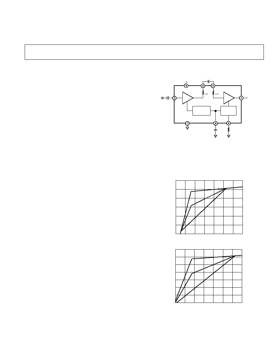
FUNCTIONAL BLOCK DIAGRAM
VCA
+1
VCA
IN
BUF
OUT
V+
V+
+
C2
10 F
BUFFER
LEVEL
DETECTOR
CONTROL
SSM2165
C1
0.1 F
AUDIO
IN+
V
OUT
R1
25k
C3
22 F
AVG CAP
COMPRESSION
RATIO SET
GND
R
A
2
R
A
2
+
FEATURES
Complete Microphone Conditioner in an 8-Lead Package
Single +5 V Operation
Preset Noise Gate Threshold
Compression Ratio Set by External Resistor
Automatic Limiting Feature Prevents ADC Overload
Adjustable Release Time
Low Noise and Distortion
20 kHz Bandwidth ( 1 dB)
Low Cost
APPLICATIONS
Microphone Preamplifier/Processor
Computer Sound Cards
Public Address/Paging Systems
Communication Headsets
Telephone Conferencing
Guitar Sustain Effects Generator
Computerized Voice Recognition
Surveillance Systems
Karaoke and DJ Mixers
GENERAL DESCRIPTION
The SSM2165 is a complete and flexible solution for condition-
ing microphone inputs in computer audio systems. It is also
excellent for improving vocal clarity in communications and
public address systems. A low noise voltage controlled amplifier
(VCA) provides a gain that is dynamically adjusted by a control
loop to maintain a set compression characteristic. The compres-
sion ratio is set by a single resistor and can be varied from 1:1 to
over 15:1 relative to the fixed rotation point. Signals above the
rotation point are limited to prevent overload and to eliminate
"popping." A downward expander (noise gate) prevents amplifi-
cation of noise or hum. This results in optimized signal levels
prior to digitization, thereby eliminating the need for additional
gain or attenuation in the digital domain that could add noise or
impair accuracy of speech recognition algorithms. The flexibility
of setting the compression ratio and the time constant of the
level detector, coupled with two values of rotation point, make
the SSM2165 easy to integrate in a wide variety of microphone
conditioning applications.
The SSM2165 is an ideal companion product for audio codecs
used in computer systems, such as the AD1845 and AD1847.
The device is available in 8-lead SOIC and P-DIP packages, and
guaranteed for operation over the extended industrial temperature
range of 40
°
C to +85
°
C. As shown in Figure 1a, the SSM2165-1
has a rotation point of 25.7 dBu (40 mV)
1
, a VCA gain of 18 dB,
and gives 7.7 dBu (320 mV) before limiting. As shown in Figure
1b, the SSM2165-2 has a rotation point of 17.8 dBu (100 mV),
a VCA gain of 8 dB and gives 9.8 dBu (250 mV) before limiting.
Both have a noise gate threshold of 64 dBu (500
µ
V), below
which downward expansion reduces the gain with a ratio of
approximately 1:3. That is, a 3 dB reduction of output signal
occurs with a 1 dB reduction of input signal. For applications
requiring adjustable noise gate threshold, VCA gain up to 18 dB,
and adjustable rotation point, please refer to the SSM2166.
INPUT dBu
OUTPUT dBu
0
10
80
70
60
50
40
30
20
10
40
50
60
20
30
Figure 1a. SSM2165-1 Compression and Gating Characteristics
INPUT dBu
OUTPUT dBu
0
10
80
70
60
50
40
30
20
10
40
50
60
70
20
30
Figure 1b. SSM2165-2 Compression and Gating Characteristics
Microphone Preamplifier with
Variable Compression and Noise Gating
*Patents pending.
1
All signals are in rms volts or dBu (0 dBu = 0.775 V rms).

REV. A
2
SSM2165SPECIFICATIONS
Parameter
Symbol
Conditions
Min
Typ
Max
Units
AUDIO SIGNAL PATH
Voltage Noise Density
e
n
15:1 Compression, V
IN
= GND
17
nV/
Hz
2
Noise
20 kHz Bandwidth, V
IN
= GND
109
dBu
1
Total Harmonic Distortion
THD+N
SSM2165-1
2nd and 3rd Harmonics, V
IN
= 30 dBu
0.2
0.5
%
SSM2165-2
2nd and 3rd Harmonics, V
IN
= 20 dBu
0.2
0.5
%
22 kHz Low-Pass Filter
Input Impedance
Z
IN
180
k
Output Impedance
Z
OUT
75
Load Drive
Resistive
5
k
Capacitive
2
nF
Input Voltage Range
1% THD
1
V rms
Output Voltage Range
1% THD
1.4
V rms
Gain Bandwidth Product
1:1 Compression
SSM2165-1
VCA G = 18 dB
300
kHz
SSM2165-2
VCA G = 8 dB
100
kHz
CONTROL SECTION
VCA Dynamic Gain Range
40
dB
VCA Fixed Gain
SSM2165-1
18
dB
SSM2165-2
8
dB
Rotation Point
SSM2165-1
40
mV rms
SSM2165-2
100
mV rms
Compression Ratio, Min
1:1
Compression Ratio, Max
15:1
Control Feedthrough
15:1 Compression
±
5
mV
POWER SUPPLY
Supply Voltage Range
V
S
4.5
5.5
V
Supply Current
I
SY
7.5
10
mA
Quiescent Output Voltage Level
2.2
V
Power Supply Rejection Ratio
2
PSRR
50
dB
NOTES
1
0 dBu = 0.775 V rms.
2
Referred to input.
Specifications subject to change without notice.
(V+ = +5 V, f = 1 kHz, R
L
= 100 k , R
COMP
= 0 , T
A
= +25 C, unless otherwise noted)
REV. A
SSM2165
3
CAUTION
ESD (electrostatic discharge) sensitive device. Electrostatic charges as high as 4000 V readily
accumulate on the human body and test equipment and can discharge without detection.
Although the SSM2165 features proprietary ESD protection circuitry, permanent damage may
occur on devices subjected to high energy electrostatic discharges. Therefore, proper ESD
precautions are recommended to avoid performance degradation or loss of functionality.
PIN FUNCTION DESCRIPTIONS
Pin #
Mnemonic
Function
1
GND
Ground
2
VCA
IN
VCA Input Pin. A typical
connection is a 1
µ
F10
µ
F
capacitor from the buffer output
pin (Pin 3) to this pin.
3
BUF
OUT
Input Buffer Amplifier Output
Pin. Must not be loaded by
capacitance to ground.
4
AUDIO +IN
Input Audio Signal. The input
signal should be ac-coupled
(0.1
µ
F typical) into this pin.
5
AVG CAP
Detector Averaging Capacitor.
A capacitor, 2.2
µ
F22
µ
F, to
ground from this pin is the
averaging capacitor for the
detector circuit.
6
COMP RATIO SET Compression Ratio Set Pin. A
resistor to ground from this pin
sets the compression ratio as
shown in Figure 1.
7
OUTPUT
Output Signal.
8
V+
Positive Supply, +5 V Nominal.
ABSOLUTE MAXIMUM RATINGS
Supply Voltage . . . . . . . . . . . . . . . . . . . . . . . . . . . . . . . . . +10 V
Audio Input Voltage . . . . . . . . . . . . . . . . . . . . . Supply Voltage
Operating Temperature Range . . . . . . . . . . . . 40
°
C to +85
°
C
Storage Temperature Range . . . . . . . . . . . . . 65
°
C to +150
°
C
Junction Temperature (T
J
) . . . . . . . . . . . . . . . . . . . . . . +150
°
C
Lead Temperature (Soldering, 60 sec) . . . . . . . . . . . . . +300
°
C
ESD RATINGS
883 (Human Body) Model . . . . . . . . . . . . . . . . . . . . . . . 2.0 kV
THERMAL CHARACTERISTICS
Thermal Resistance
8-Lead Plastic DIP
JA
. . . . . . . . . . . . . . . . . . . . . . . . . . . . . . . . . . . 103
°
C/W
JC
. . . . . . . . . . . . . . . . . . . . . . . . . . . . . . . . . . . . 43
°
C/W
8-Lead SOIC
JA
. . . . . . . . . . . . . . . . . . . . . . . . . . . . . . . . . . . 158
°
C/W
JC
. . . . . . . . . . . . . . . . . . . . . . . . . . . . . . . . . . . . 43
°
C/W
ORDERING GUIDE
Temperature
Package
Package
Model
Range
Description
Options
SSM2165-1P
40
°
C to +85
°
C
Plastic DIP
N-8
SSM2165-2P
40
°
C to +85
°
C
Plastic DIP
N-8
SSM2165-1S
40
°
C to +85
°
C
Narrow SOIC
SO-8
SSM2165-2S
40
°
C to +85
°
C
Narrow SOIC
SO-8
PIN CONFIGURATION
1
2
3
4
8
7
6
5
GND
AVG CAP
COMP RATIO SET
OUTPUT
V+
VCA
IN
BUF
OUT
AUDIO +IN
TOP VIEW
(Not to Scale)
SSM2165
WARNING!
ESD SENSITIVE DEVICE
REV. A
SSM2165
4
COMPRESSION RATIO
1:1
15:1
2:1
5:1
10:1
160
120
200
40
80
0
T
A
= +25 C
V
S
= +5V
R
L
= 100k
SSM21651
R
COMP
k
SSM21652
220
20
240
260
60
100
140
180
Figure 2. Compression Ratio vs. R
COMP
INPUT V rms
1
0.1
0.01
1
THD+N %
0.1
5
T
A
= +25 C
COMP RATIO = 1:1
R
L
= 100k /10k
V
S
= +5V
SSM21652
SSM21651
0.050
Figure 3. THD + N (%) vs. Input (V rms)
FREQUENCY Hz
1
0.1
20
30k
100
THD+N %
1k
10k
5
T
A
= +25 C
V
S
= +5V
COMP RATIO = 1:1
V
I N
= 20dBu (1)
V
I N
= 30dBu (2)
R
L
= 100k
SSM21652
SSM21651
0.050
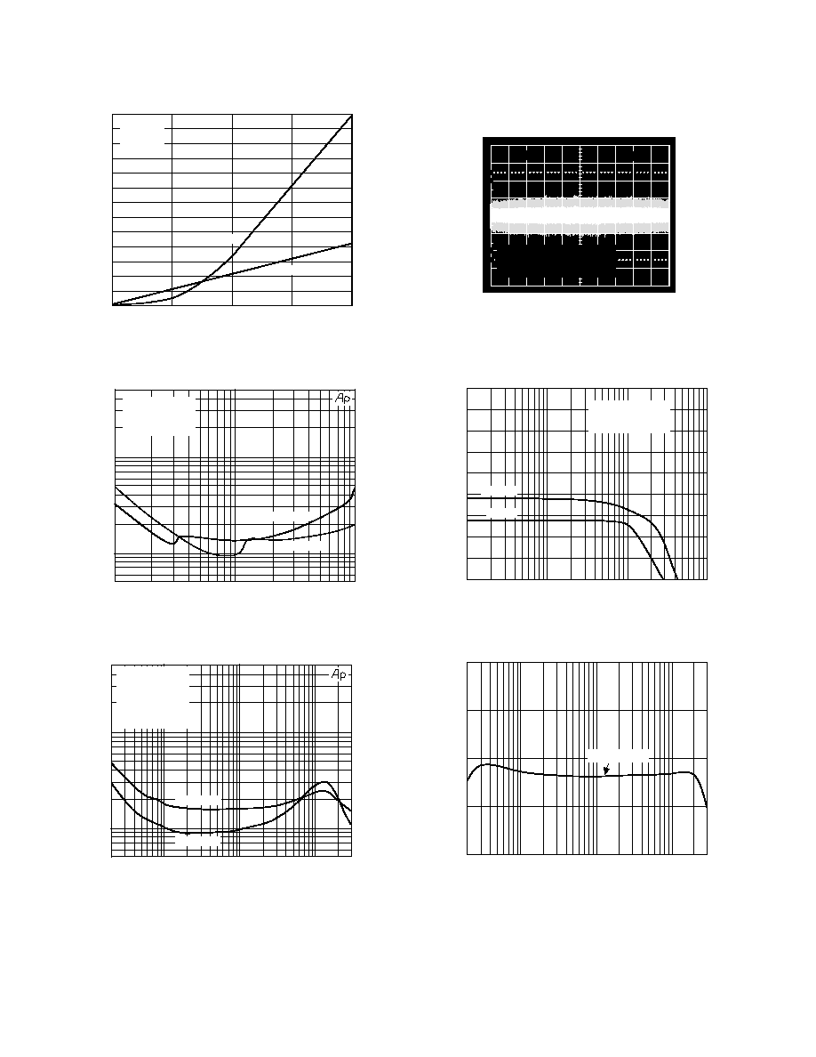
Figure 4. THD + N (%) vs. Frequency (Hz)
10
0%
100
90
1s
5 V
T
A
= +25 C
COMPRESSION RATIO = 15:1
NOISE BW = 20kHz
Figure 5. Wideband Output Noise
FREQUENCY Hz
GAIN dB
70
60
20
1k
1M
10k
100k
50
40
0
30
20
10
10
COMP RATIO = 15:1
R
COMP
= 0
V
IN
= 40 V rms
G = 18dB
G = 8dB
Figure 6. GBW Curves vs. VCA Gain
FREQUENCY Hz
20
30k
100
1k
30
40
50
60
70
10k
PSRR dB
V+ = 5 1V p-p
Figure 7. PSRR vs. Frequency, Referred to Input
Typical Performance Characteristics
REV. A
SSM2165
5
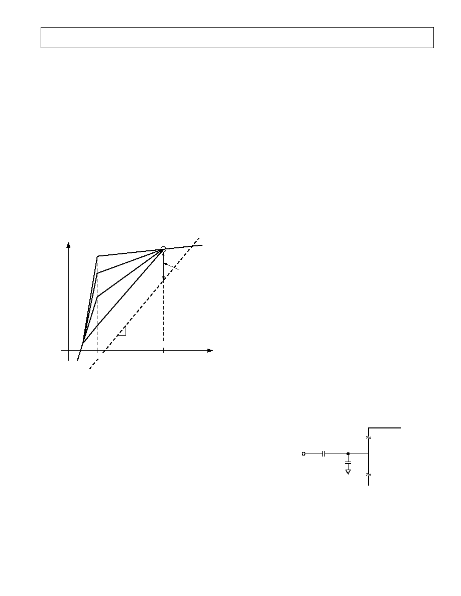
THEORY OF OPERATION
Figure 10 illustrates the general transfer characteristic for the
SSM2165 where the output level in dBu is plotted as a function
of the input level in dBu (0 dBu = 0.775 V rms). For input
signals in the range of V
DE
(Downward Expansion) to V
RP
(Rotation Point) an "r" dB change in the input level causes a
1 dB change in the output level. Here, "r" is defined as the
"compression ratio." The compression ratio may be varied
from 1:1 (no compression) to over 15:1 via a single resistor,
R
COMP
. Input signals above V
RP
are compressed with a fixed
compression ratio of approximately 10:1. This region of opera-
tion is the "limiting region." Varying the compression ratio has
no effect on the limiting region. The breakpoint between the
compression region and the limiting region is referred to as the
"limiting threshold" or "rotation point," and is different for the
SSM2165-1 and SSM2165-2, see Table I.
Table I. Characteristics vs. Dash Number
SSM2165
Rotation Point
Gain
Output*
1
40 mV (25.7 dBu)
18 dB
320 mV (6 dBu)
2
100 mV (17.7 dBu)
8 dB
250 mV (8 dBu)
*At limiting.
The term "rotation point" derives from the observation that the
straight line in the compression region "rotates" about this point
on the input/output characteristic as the compression ratio is
changed.
When the compression is set to 2:1, a 2 dB change of the
input signal level in the compression region causes 1 dB
change of the output level. Likewise, at 10:1 compression, a
10 dB change of the input signal level in the compression
region causes a 1 dB change in the output level. The gain of
the system with an input signal level of V
RP
is fixed regardless of
the compression ratio, and is different for the SSM2165-1 and
SSM2165-2 (see Figures 1a and 1b). The "nominal gain" of
the system is 18 dB for the SSM2165-1, and 8 dB for the
SSM2165-2. System gain is measured at V
RP
and is (V
OUT
V
IN
)
in dB.
Input signals below V
DE
are downward expanded at a ratio of
approximately 1:3. As a result, the gain of the system is small
for very small input signal levels below V
DE
, even though it may
be quite large for input signals above V
DE
. The downward
expansion threshold, V
DE
, is fixed at 500
µ
V (64 dBu) for both
dash versions.
APPLICATIONS INFORMATION
The SSM2165 is a complete microphone signal conditioning
system in a single integrated circuit. Designed primarily for
voiceband applications, this integrated circuit provides amplifi-
cation, rms detection, limiting, variable compression, and down-
ward expansion. The internal rms detector has a time constant
set by an external capacitor. An integral voltage-controlled
amplifier (VCA) provides up to 40 dB of gain in the signal path
with approximately 30 kHz bandwidth. The device operates on
a single +5 V supply, accepts input signals up to 1 V
1
, and pro-
duces output signal levels at limiting of 320 mV and 250 mV for
the SSM2165-1 and SSM2165-2 respectively, into loads > 5 k
.
The SSM2165 contains an input buffer and automatic gain
control (AGC) circuit for audio and voice band signals. Circuit
operation is optimized by providing user-adjustable compression
ratio and time constant. A downward expansion (noise gating)
feature reduces background and circuit noise below 500
µ
V.
The rotation point determines the output signal levels before
limiting (referred to the input), and is 40 mV for the SSM2165-1
and 100 mV for the SSM2165-2.
INPUT dB
OUTPUT dB
LIMITING
REGION
LIMITING
THRESHOLD
(ROTATION POINT)
COMPRESSION
REGION
1
r
1
1
DOWNWARD
EXPANSION
THRESHOLD
(NOISE GATE)
DOWNWARD
EXPANSION
REGION
V
rp
VCA GAIN
V
DE
Figure 10. General Input/Output Characteristics of the
SSM2165
10
0%
100
90
20mV
10 s
T
A
= +25 C
C
AVG
= 2.2 F
R
L
= 10k
COMP RATIO = 1:1
V
IN
= 12.5mV (1)
V
IN
= 40mV (2)
Figure 8. Small Signal Transient Response
10
0%
100
90
10 s
200mV
T
A
= +25 C
C
AVG
= 2.2 F
R
L
= 10k
COMP RATIO = 1:1
V
IN
= 125mV (1)
V
IN
= 400mV (2)
Figure 9. Large Signal Transient Response
1
All signals are in rms volts or dBu (0 dBu = 0.775 V rms).
REV. A
SSM2165
6
operation of the level detector down to 10 Hz, the value of the
capacitor should be around 22
µ
F. Some experimentation with
larger values for the AVG CAP may be necessary to reduce the
effects of excessive low frequency ambient background noise.
The value of the averaging capacitor affects sound quality: too
small a value for this capacitor may cause a "pumping effect"
for some signals, while too large a value can result in slow re-
sponse times to signal dynamics. Electrolytic capacitors are
recommended here for lowest cost.
The rms detector filter time constant is approximately given by
10
×
C
AVG
milliseconds where C
AVG
is in
µ
F. This time con-
stant controls both the steady-state averaging in the rms detec-
tor as well as the release time for compression, that is, the time
it takes for the system gain to react when a large input is fol-
lowed by a small signal. The attack time, the time it takes for
the gain to be reduced when a small signal is followed by a large
signal, is mainly controlled by internal circuitry that speeds up
the attack for large level changes, and controlled partly by the
AVG CAP value. This limits overload time to under 1 ms in
most cases.
The performance of the rms level detector is illustrated in Fig-
ure 12 for C
AVG
= 2.2
µ
F and Figure 13 for C
AVG
= 22
µ
F. In
each of these photographs, the input signal to the SSM2165
(not shown) is a series of tone bursts in 6 successive 10 dB
steps. The tone bursts range from 66 dBu (0.5 mV rms) to
6 dBu (0.5 V rms). As illustrated in the photographs, the
attack time of the rms level detector is dependent only on C
AVG
,
but the release times are linear ramps whose decay times are
dependent on both for C
AVG
and the input signal step size. The
rate of release is approximately 240 dB/s for a C
AVG
= 2.2
µ
F,
and 12 dB/s for a C
AVG
of 22
µ
F.
10
0%
100
90
100mV
100ms
6dBV
66dBV
85dBV
Figure 12. RMS Level Detector Performance with
C
AVG
= 2.2
µ
F
10
0%
100
90
100mV
1s
6dBV
66dBV
85dBV
Figure 13. RMS Level Detector Performance with
C
AVG
= 22
µ
F
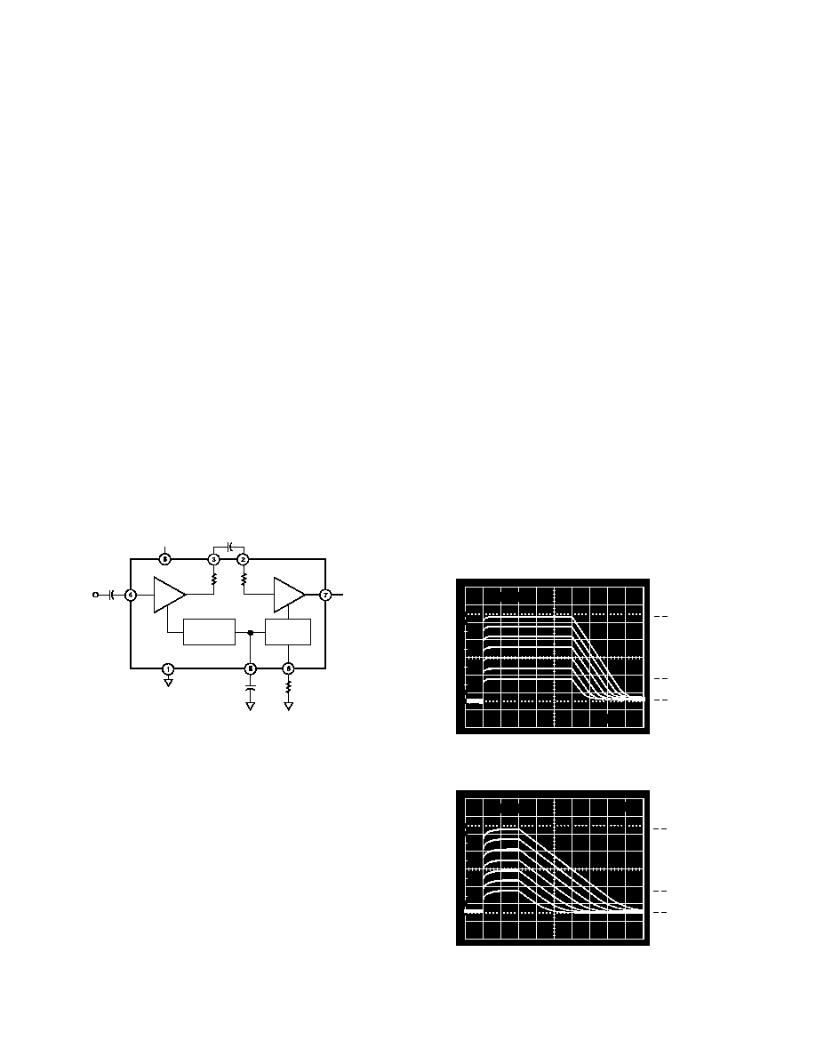
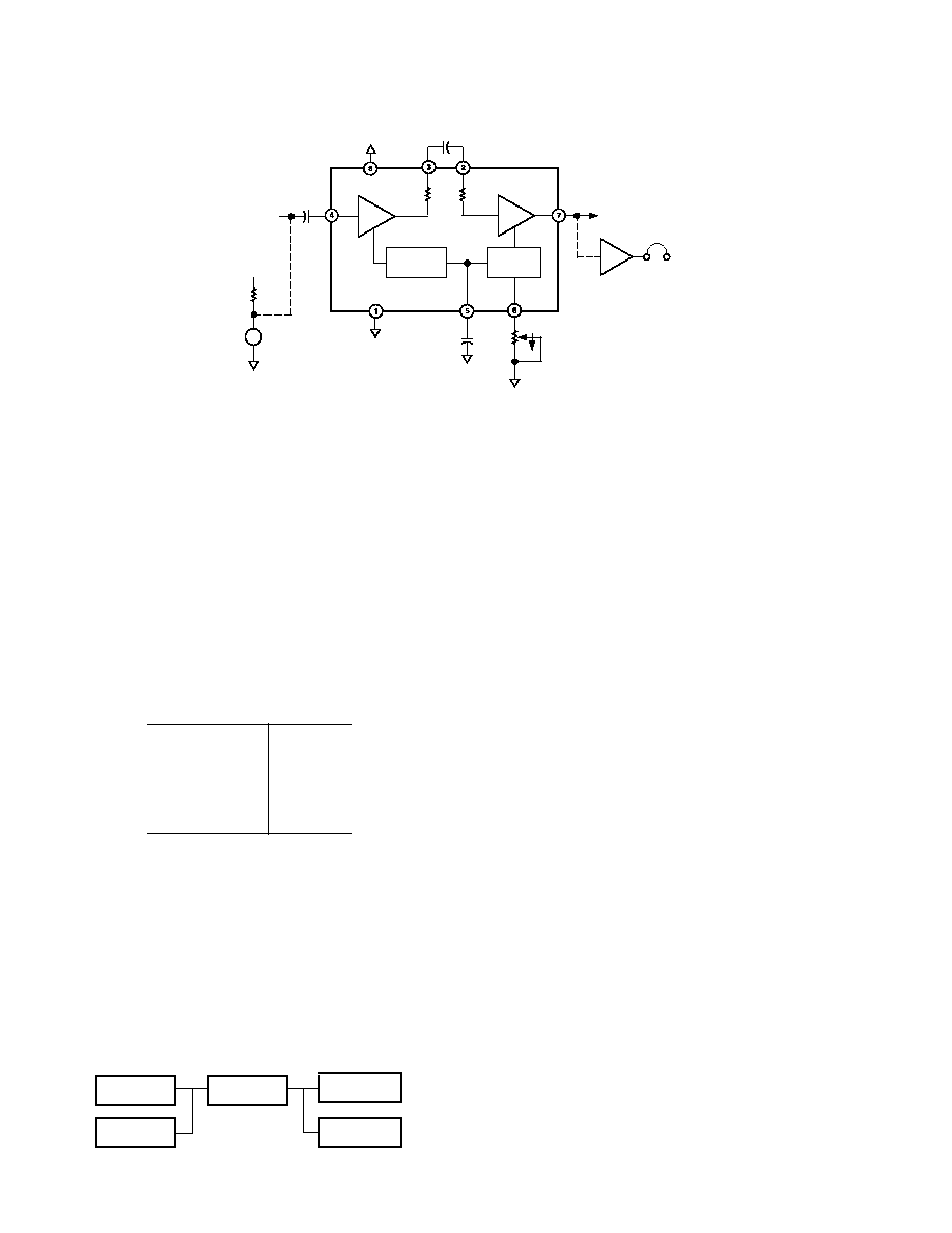
The SSM2165 Signal Path
Figure 11 illustrates the block diagram of the SSM2165. The
audio input signal is processed by the unity gain input buffer
and then by the VCA. The buffer presents an input impedance
of approximately 180 k
to the source. A dc voltage of approxi-
mately 1.5 V is present at AUDIO +IN (Pin 4), requiring the
use of a blocking capacitor (C1) for ground-referenced sources.
A 0.1
µ
F capacitor is a good choice for most audio applications.
The buffer is designed to drive only the low impedance input of
the VCA, and must not be loaded by capacitance to ground.
The VCA is a low distortion, variable-gain amplifier whose gain
is set by the internal control circuitry. The input to the VCA is
a virtual ground in series with 500
. An external blocking
capacitor (C2) must be used between the buffer's output and
the VCA input. The desired low frequency response and the
total of 1 k
impedance between amplifiers determines the
value of this capacitor. For music applications, 10
µ
F will give
high pass f
C
= 16 Hz. For voice/communications applications,
1
µ
F will give f
C
= 160 Hz. An aluminum electrolytic capacitor
is an economical choice. The VCA amplifies the input signal
current flowing through C6 and converts this current to a
voltage at the SSM2165's output (Pin 7). The net gain from
input to output can be as high as 40 dB for high compression
ratios and depending on the gain set by the control circuitry.
The output impedance of the SSM2165 is typically less than
75
, and the external load on Pin 7 should be >5 k
. The
nominal output dc voltage of the device is approximately 2.2 V.
Use a dc blocking capacitor for grounded loads.
VCA
+1
VCA
IN
BUF
OUT
V+
V+
+
C2
10 F
BUFFER
LEVEL
DETECTOR
CONTROL
SSM2165
C1
0.1 F
AUDIO
IN+
V
OUT
R1
25k
C3
22 F
AVG CAP
COMPRESSION
RATIO SET
GND
+
500
500
Figure 11. Functional Block Diagram and Typical Voice
Application
The bandwidth of the SSM2165 is quite wide at all gain set-
tings. The upper 3 dB point is approximately 300 kHz. The
GBW plots are shown in Figure 6. While the noise of the input
buffer is fixed, the input referred noise of the VCA is a function
of gain. The VCA input noise is designed to be a minimum
when the gain is at a maximum, thereby optimizing the usable
dynamic range of the part. A photograph of the SSM2165's
wideband peak-to-peak output noise is illustrated in Figure 5.
The Level Detector
The SSM2165 incorporates a full-wave rectifier and a patent-
pending, true rms level detector circuit whose averaging time
constant is set by an external capacitor connected to the AVG
CAP pin (Pin 5). Capacitor values from 18
µ
F to 22
µ
F have
been found to be more appropriate in voiceband applications,
where capacitors on the low end of the range seem more appro-
priate for music program material. For optimal low frequency
REV. A
SSM2165
7
Control Circuitry
The output of the rms level detector is a signal proportional to
the log of the true rms value of the buffer output with an added
dc offset. The control circuitry subtracts a dc voltage from this
signal, scales it, and sends the result to the VCA to control the
gain. The VCA's gain control is logarithmic: a linear change in
control signal causes a dB change in gain. It is this control law
that allows linear processing of the log rms signal to provide the
flat compression characteristic on the input/output characteris-
tic shown in Figure 10.
Compression Ratio
Changing the scaling of the control signal fed to the VCA
causes a change in the circuit's compression ratio, "r." This
effect is shown in Figure 14. The compression ratio can be set
by connecting a resistor between the COMP RATIO pin (Pin
6) and GND. Lowering RCOMP gives smaller compression
ratios as indicated in Figure 2, with values of about 5 k
or less
resulting in a compression ratio of 1:1. AGC performance is
achieved with compression ratios between 2:1 and 15:1, and is
dependent on the application. A 200 k
potentiometer may be
used to allow this parameter to be adjusted.
INPUT dB
OUTPUT dB
V
DE
V
RP
15:1
5:1
2:1
1:1
1
1
VCA GAIN
Figure 14. Effect of Varying the Compression Ratio
Rotation Point
An internal dc reference voltage in the control circuitry sets the
rotation point. The rotation point determines the output level
above which limiting occurs. That is, in the limiting region, a
10 dB change of input results in a 1 dB change of output. The
rotation point is set to 40 mV (26 dBu) for the SSM2165-1
and 100 mV (18 dBu) for the SSM2165-2. In the SSM2165,
limiting is compression at a fixed compression ratio of approxi-
mately 15:1. The fixed gain in the VCA is 18 dB for the
SSM2165-1 and 8 dB for the SSM2165-2. The output signals
at limiting are, therefore, 320 mV and 250 mV respectively.
These are summarized in Table I.
Maximum Output
Since limiting occurs for signals larger than the rotation point
(V
IN
> V
RP
), the rotation point effectively sets the maximum
output signal level. The application will determine which ver-
sion of the SSM2165 should be selected. The output level
should match the maximum input allowed by the following
stage. Occasional larger signal transients will then be attenuated
by the action of the limiter.
Downward Expansion Threshold
The downward expansion threshold, or noise gate, is deter-
mined by a reference voltage internal to the control circuitry.
The noise gate threshold is 500
µ
V for both versions of the
SSM2165. Users requiring some other noise gate should con-
sider using the SSM2166. High volume users may wish to con-
sider a custom version of the SSM2165 with other noise gate
thresholds or rotation points.
Power-On/Power-Off Settling Time
Cycling the power supply to the SSM2165 will result in quick
settling times: the off-on settling time of the SSM2165 is less
than 200 ms, while the on-off settling time is less than 1 ms.
Note that transients may appear at the output of the device
during power up and power down. A clickless mute function is
available on the SSM2166 only.
PC Board Layout Considerations
Since the SSM2165 is capable of wide bandwidth operation at
high gain, special care must be exercised in the layout of the PC
board which contains the IC and its associated components.
The following applications hints should be considered and/or
followed:
1. In some high system gain applications, the shielding of input
wires to minimize possible feedback from the output of the
SSM2165 back to the input circuit may be necessary.
2. A single-point ("star") ground implementation is recom-
mended in addition to maintaining short lead lengths and
PC board runs. In systems where an analog ground and a
digital ground are available, the SSM2165 and its surround-
ing circuitry should be connected to the analog ground.
Wire-wrap board connections and grounding implementa-
tions are to be explicitly avoided.
3. The internal buffer of the SSM2165 was designed to drive
only the input of the internal VCA and its own feedback
network. Stray capacitive loading to ground from either Pin
3 or Pin 2 in excess of 5 pF to 10 pF can cause excessive
phase shift and can lead to circuit instability.
4. When using high impedance sources, it can be advantageous
to shunt the source with a capacitor to ground at the input
pin of the IC (Pin 4) to lower the source impedance at high
frequencies, as shown in Figure 15. A capacitor with a value
of 1000 pF is a good starting value and sets a low pass corner
at 31 kHz for 5 k
sources.
C
X
1000pF
C1
0.1 F
AUDIO IN
(R
S
> 5k )
4
+IN
SSM2165
NOTE: ADDITIONAL CIRCUIT DETAILS
OMITTED FOR CLARITY.
Figure 15. Circuit Configuration for Use with High
Impedance Signal Sources
REV. A
SSM2165
8
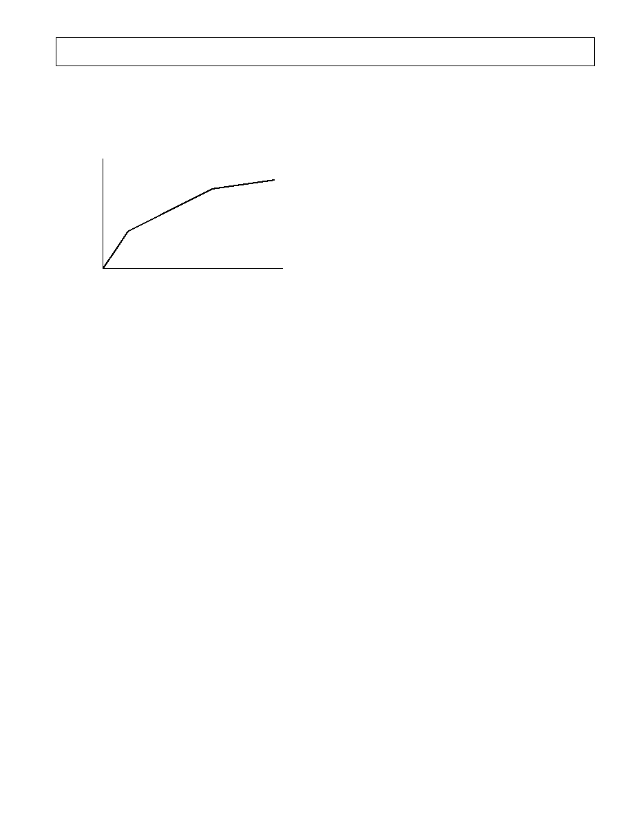
Compression Adjustment--A Practical Example
To illustrate how to set the compression ratio of the SSM2165,
we will take a practical example. The SSM2165 will be used
interface an electret-type microphone to a post-amplifier, as
shown in Figure 16. The signal from the microphone was mea-
sured under actual conditions to vary from 2 mV to 30 mV.
The post-amplifier requires no more than 350 mV at its input.
We will therefore choose the SSM2165-1, whose "rotation"
point is 40 mV and whose VCA fixed gain is 18 dB (
×
8), thus
giving 320 mV at limiting. From prior listening experience, we
will use a 2:1 compression ratio. The noise gate threshold of the
SSM2165-1 will operate when the input signal falls below 500
µ
V.
These objectives are summarized in Table II. The transfer charac-
teristic we will implement is illustrated in Figure 18.
Table II. Objective Specification of Example
Input Range
2 mV30 mV
Output Range
To 350 mV
Limiting Level
320 mV
Compression
2:1
Gain
18 dB
Noise Gate
500
µ
V
Test Equipment Setup
The recommended equipment and configuration is shown in
Figure 17. A low noise audio generator with a smooth output
adjustment range of 100
µ
V to 25 mV is a suitable signal
source. The output voltmeter should go up to 2 volts. The
oscilloscope is used to verify that the output is sinusoidal, that
no clipping is occurring in the buffer, and to observe the limit-
ing and noise gating "knees."
Breadboard Considerations
When building your breadboard, keep the leads to Pins 2 and 3
as short as possible. Use a central analog ground and decouple
power supply connections adequately.
SIGNAL
GENERATOR
SSM2165-1
AC
VOLTMETER
OSCILLOSCOPE
AC
VOLTMETER
Figure 17. Test Equipment Setup
+1
VCA
IN
BUF
OUT
+5V
V+
+
C2
10 F
BUFFER
LEVEL
DETECTOR
CONTROL
SSM2165-1
C1
0.1 F
GENERATOR
AND AC
VOLTMETER
200k
C3
22 F
AVG CAP
1:1
R1 COMPRESSION
15:1 RATIO SET
GND
+2V
2k
MICROPHONE
(ELECTRET)
+
CW
HEADPHONES
AC VOLTMETER
AND OSCILLOSCOPE
+
VCA
Figure 16. Electret Microphone Preamp Example
STEP 1. Initialize Potentiometer
With power off, preset R1--Compression Ratio potentiometer
to zero ohms.
STEP 2. Check Setup
With power on, adjust the generator for an input level of
50 mV (24 dBu), 1 kHz. The output meter should indicate
approximately 350 mV (6.9 dBu). If not, check your setup.
STEP 3. Find the Rotation Point
Set the input level to 50 mV (24 dBu), and observe the output
on the oscilloscope. The output will be in the limiting range of
operation. Slowly reduce the input signal level until the output
level just begins to stop limiting and follows the input down.
Increase the input so that the output is 320 mV (7.7 dBu). You
have located the knee of the rotation point.
STEP 4. Adjust the Compression Ratio
With the input set as in Step 3, note the exact value of the input
signal level just below the knee (around 40 mV (26 dBu)).
Next, reduce the input to 1/4 the value noted, (around 10 mV
(38 dBu)), for a change of 12 dB. Next, increase the R
COMP
potentiometer resistance so the output is 160 mV (13.7 dBu)
for an output change of 6 dB. You have now set the compres-
sion, which is the ratio of input change to output change, in dB,
to 2:1.
STEP 5. Confirm the Noise Gate Threshold
Set the input to 1 mV, and observe the output on the oscillo-
scope. A 20 dB pad between generator and input may facilitate
this measurement. Reduce the input gradually until the output
falls off more rapidly. This point is the noise gate threshold, and
should be approximately 500
µ
V (64 dBu). The noise gate
threshold on the SSM2165 is fixed at 500
µ
V, a practical value
for many microphones. Should you require a different noise gate
threshold, consider using the SSM2166.
STEP 6. Listen
At this time, you may replace the signal generator with a
properly powered electret microphone and listen to the results
through a set of headphones. The microphone's internal FET
usually requires around +2 V through a 2 k
resistor; this varies
with the manufacturer. Experiment with the compression ratio
value and averaging capacitor size. More compression will keep
the output steady over a wider range of microphone-to-source
distance. Varying the averaging capacitor, C
AVG
, changes the
REV. A
SSM2165
9
rms detector averaging time, and the decay time of the gate.
Both compression ratio and decay time are usually determined
by critical listening to the intended audio input.
STEP 7. Record Values
With the power removed from the test fixture, measure and
record the values of the
R
COMP
and C
AVG.
OUTPUT mV
300
45
COMPRESSION
REGION
LIMITING REGION
NOISE GATING REGION
0.5
2
30
40
INPUT mV
Figure 18. Transfer Characteristic
SUMMARY
We have implemented the transfer characteristic of Figure 18.
For inputs below the 500
µ
V noise gate threshold, circuit and
background noise will be downward expanded (gain-reduced) at
a ratio of approximately 1:3. That is, a 1 dB change in the
noise will result in 3 dB decrease at the output. Above thresh-
old, the signal will increase at a rate of 1 dB for each 2 dB input
increase, until the rotation point is reached at an input of
approximately 40 mV. In the limiting region, the compression
ratio increases to approximately 15:1. That is, a 15 dB increase
in input will produce a 1 dB increase at the output, so there will
be little further increase for higher level inputs.
Other Versions
The SSM2165 is an 8-lead version of the 14-lead SSM2166
which is recommended for applications requiring more versatil-
ity. The SSM2166 allows selection of noise gate threshold and
rotation point, and allows the buffer to provide up to 20 dB of
gain. Power-down and mute functions are also built in. Custom-
ized versions of the SSM2165 are available for large volume
users. The wide dynamic range of the SSM2165 makes it useful
in many applications other than microphone signal conditioning
such as a sustain generator for guitars. For further information,
contact your Analog Devices representative.
REV. A
SSM2165
10
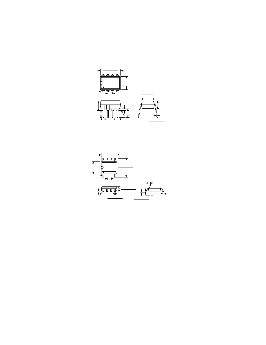
OUTLINE DIMENSIONS
Dimensions shown in inches and (mm).
8-Lead Plastic DIP
(N-8)
SEATING
PLANE
0.060 (1.52)
0.015 (0.38)
0.210
(5.33)
MAX
0.022 (0.558)
0.014 (0.356)
0.160 (4.06)
0.115 (2.93)
0.070 (1.77)
0.045 (1.15)
0.130
(3.30)
MIN
8
1
4
5
PIN 1
0.280 (7.11)
0.240 (6.10)
0.100 (2.54)
BSC
0.430 (10.92)
0.348 (8.84)
0.195 (4.95)
0.115 (2.93)
0.015 (0.381)
0.008 (0.204)
0.325 (8.25)
0.300 (7.62)
8-Lead Narrow-Body SOIC
(SO-8)
8
5
4
1
0.1968 (5.00)
0.1890 (4.80)
0.2440 (6.20)
0.2284 (5.80)
PIN 1
0.1574 (4.00)
0.1497 (3.80)
0.0500 (1.27)
BSC
0.0688 (1.75)
0.0532 (1.35)
SEATING
PLANE
0.0098 (0.25)
0.0040 (0.10)
0.0192 (0.49)
0.0138 (0.35)
0.0098 (0.25)
0.0075 (0.19)
0.0500 (1.27)
0.0160 (0.41)
8
0
0.0196 (0.50)
0.0099 (0.25)
45
C2178a06/99
PRINTED IN U.S.A.