Äîêóìåíòàöèÿ è îïèñàíèÿ www.docs.chipfind.ru
REV. A
Information furnished by Analog Devices is believed to be accurate and
reliable. However, no responsibility is assumed by Analog Devices for its
use, nor for any infringements of patents or other rights of third parties that
may result from its use. No license is granted by implication or otherwise
under any patent or patent rights of Analog Devices.
a
SSM2167
One Technology Way, P.O. Box 9106, Norwood, MA 02062-9106, U.S.A.
Tel: 781/329-4700
www.analog.com
Fax: 781/326-8703
© Analog Devices, Inc., 2002
Low Voltage Microphone
Preamplifier with Variable
Compression and Noise Gating
FEATURES
Complete Microphone Conditioner in a 10-Lead Package
Single 3 V Operation
Low Shutdown Current < 2 A
Adjustable Noise Gate Threshold
Adjustable Compression Ratio
Automatic Limiting Feature Prevents ADC Overload
Low Noise and Distortion: 0.2% THD + N
20 kHz Bandwidth
APPLICATIONS
Desktop, Portable, or Palmtop Computers
Telephone Conferencing
Communication Headsets
Two-Way Communications
Surveillance Systems
Karaoke and DJ Mixers
GENERAL DESCRIPTION
The SSM2167 is a complete and flexible solution for conditioning
microphone inputs in personal electronics and computer audio
systems. It is also excellent for improving vocal clarity in communi-
cations and public address systems. A low noise voltage controlled
amplifier (VCA) provides a gain that is dynamically adjusted by a
control loop to maintain a set compression characteristic. The
compression ratio is set by a single resistor and can be varied from
1:1 to over 10:1 relative to the fixed rotation point. Signals above
the rotation point are limited to prevent overload and to eliminate
"popping." A downward expander (noise gate) prevents amplifica-
tion of background noise or hum. This results in optimized signal
levels prior to digitization, thereby eliminating the need for addi-
tional gain or attenuation in the digital domain. The flexibility of
setting the compression ratio and the time constant of the level
detector, coupled with two values of rotation point, make the
SSM2167 easy to integrate in a wide variety of microphone
conditioning applications.
The SSM2167 is available in two versions, with different amounts
of fixed gain. The SSM2167-1 has 18 dB of fixed gain, while
the SSM2167-2 features only 8 dB of fixed gain.
The device is available in 10-lead MSOP package, and guaranteed
for operation over the extended industrial temperature range of
40
°C to +85°C.
PIN CONFIGURATION
10-Lead MSOP
(RM Suffix)
INPUT dB
OUTPUT dB
LIMITING
REGION
LIMITING
THRESHOLD
(ROTATION POINT)
COMPRESSION
REGION
1
r
1
1
DOWNWARD
EXPANSION
THRESHOLD
(NOISE GATE)
DOWNWARD
EXPANSION
REGION
V
DE
V
RP
VCA GAIN
Figure 1. General Input/Output Characteristics
SSM2167
GND
VCA
IN
SHUTDOWN
BUF OUT
INPUT
V
DD
OUTPUT
COMPRESSION RATIO
GATE THRS
AVG CAP
1
2
3
4
5
10
9
8
7
6

REV. A
2
SSM2167SPECIFICATIONS
(@ V
S
= 3.0 V, f = 1 kHz, R
L
= 100 k
, R
COMP
= 0
, T
A
= 25 C, V
IN
= 100 mV rms,
R
GATE
= 2 k
, unless otherwise noted.)
Parameter
Symbol
Conditions
Min
Typ
Max
Unit
AUDIO SIGNAL PATH
Voltage Noise Density
e
n
10:1 Compression
20
nV
/Hz
Noise
20 kHz Bandwidth, V
IN
= GND
70
dBV
Total Harmonic Distortion + Noise
THD + N
V
IN
= 100 mV rms
0.2
%
Input Impedance
Z
IN
100
k
Output Impedance
Z
OUT
145
Load Drive
Minimum Resistive Load
5
k
Maximum Capacitive Load
2
nF
Input Voltage Range
0.4% THD
600
mV rms
Output Voltage Range
0.4% THD
SSM2167-1
700
mV rms
SSM2167-2
*
700
mV rms
Gain Bandwidth Product
1:1 Compression
SSM2167-1
VCA G = 18 dB
1
MHz
SSM2167-2
*
VCA G = 8 dB
1
MHz
CONTROL SECTION
VCA Dynamic Gain Range
40
dB
VCA Fixed Gain
SSM2167-1
18
dB
SSM2167-2
*
8
dB
Compression Ratio, Min
1:1
Compression Ratio, Max
See Table I for R
COMP
10:1
Rotation Point
SSM2167-1
63
mV rms
SSM2167-2
*
100
mV rms
Noise Gate Range
Maximum Threshold
40
dBV
POWER SUPPLY
Supply Voltage
V
SY
2.5
5.5
V
Supply Current
I
SY
2.3
5
mA
DC Output Voltage
1.4
V
Power Supply Rejection Ratio
PSRR
V
SY
= 2.5 V to 6 V
4.5
mV
SHUTDOWN
Supply Current
I
SY
Pin 3 = GND
2
8
A
*Preliminary
Specifications subject to change without notice.
REV. A
3
SSM2167
ABSOLUTE MAXIMUM RATINGS
*
Supply Voltage . . . . . . . . . . . . . . . . . . . . . . . . . . . . . . . . . . 6 V
Input Voltage . . . . . . . . . . . . . . . . . . . . . . . . . . . . . . . . . . . 6 V
Operating Temperature Range . . . . . . . . . . . 40
°C to +85°C
Junction Temperature Range . . . . . . . . . . . . . . . . . . . . 150
°C
Lead Temperature Range (Soldering, 10 sec) . . . . . . . 300
°C
ESD RATINGS
883 (Human Body) Model . . . . . . . . . . . . . . . . . . . . . . 500 V
*Stresses above those listed under Absolute Maximum Ratings may cause perma-
nent damage to the device. This is a stress rating only; functional operation of the
device at these or any other conditions above those listed in the operational sections
of this specification is not implied. Exposure to absolute maximum rating condi-
tions for extended periods may affect device reliability.
Package Type
JA
*
JC
Unit
10-Lead MSOP (RM)
180
35
°C/W
*
JA
is specified for worst-case conditions, i.e.,
JA
is specified for device soldered
in 4-layer circuit board for surface-mount packages.
CAUTION
ESD (electrostatic discharge) sensitive device. Electrostatic charges as high as 4000 V readily
accumulate on the human body and test equipment and can discharge without detection. Although
the SSM2167 features proprietary ESD protection circuitry, permanent damage may occur on
devices subjected to high-energy electrostatic discharges. Therefore, proper ESD precautions are
recommended to avoid performance degradation or loss of functionality.
WARNING!
ESD SENSITIVE DEVICE
ORDERING GUIDE
Temperature
Package
Package
Model
Range
Description
Option
SSM2167-1RM-Reel
40
°C to +85°C
10-Lead Mini/micro SOIC (MSOP)
RM-10
SSM2167-2RM-Reel
* 40
°C to +85°C
10-Lead Mini/micro SOIC (MSOP)
RM-10
*Preliminary
REV. A
SSM2167
4
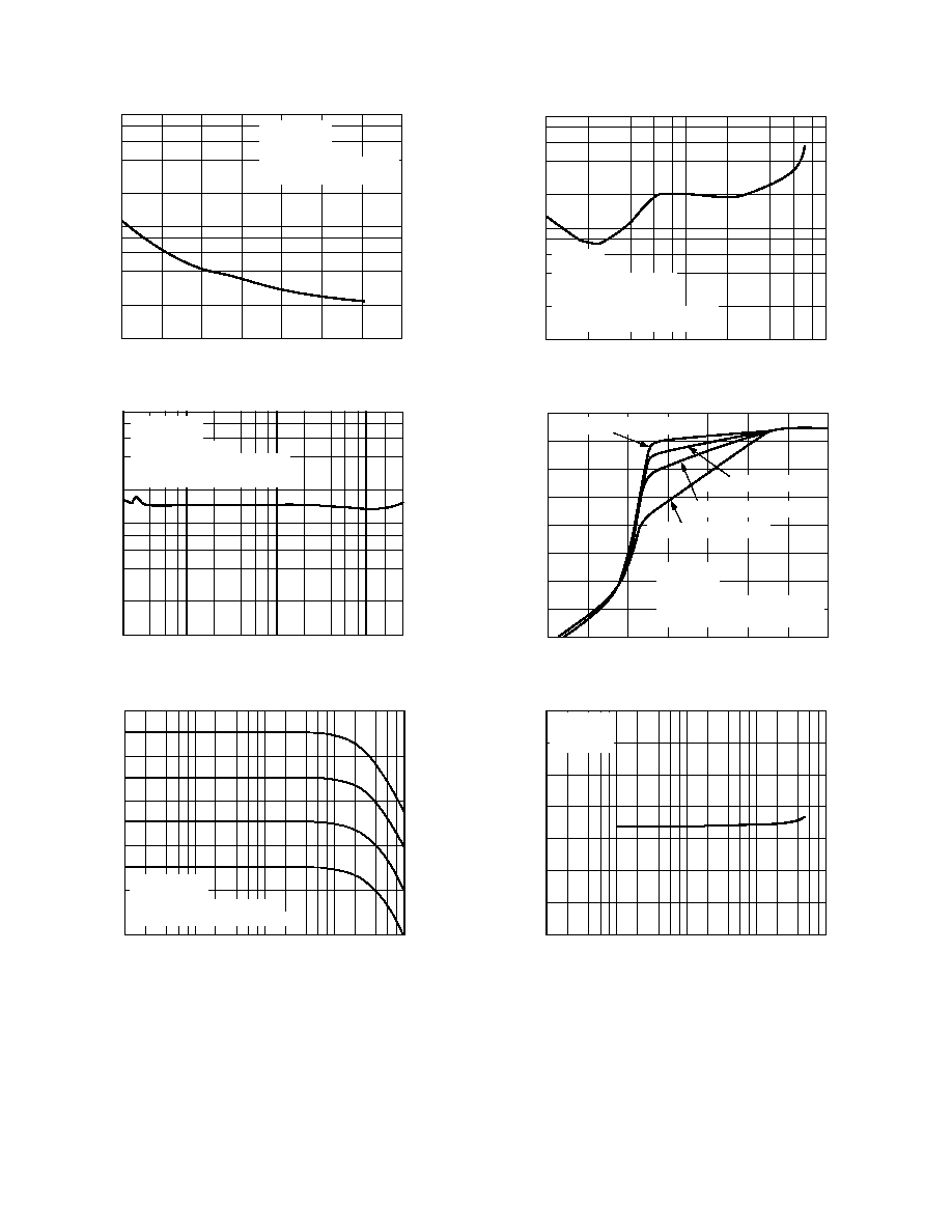
Typical Performance Characteristics
R
GATE
100
10
1
0
3,500
500
NOISE GA
TE
mV rms
1,000
1,500
2,500
2,000
3,000
T
A
= 25 C
V+ = 3V
R
LOAD
= 100k
COMPRESSION RATIO 2:1
ROTATION POINT = 63mV rms
TPC 1. Noise Gate vs. R
GATE
FREQUENCY Hz
20
30k
THD + N
%
100
1k
10k
1
0.01
0.1
20k
T
A
= 25 C
V+ = 3V
V
IN
= 24.5mV rms
COMPRESSION RATIO 1:1
ROTATION POINT = 63mV rms
NOISE GATE SETTING = 1.4mV rms
TPC 2. THD + N vs. Frequency
FREQUENCY Hz
1k
10M
10k
GAIN
dB
100k
1M
35
15
5
15
5
25
V
IN
= 2mV rms
R
COMP
= 175k
ROTATION POINT = 63mV rms
NOISE GATE SETTING = 1.4mV rms
TPC 3. GBW Curves vs. VCA Gain
INPUT VOLTAGE V rms
1
0.1
0.01
10m
1
0.1
THD + N
%
T
A
= 25 C
V+ = 3V
V
IN
FREQUENCY = 1kHz
R
LOAD
= 100k
COMPRESSION RATIO 1:1
ROTATION POINT = 63mV rms
NOISE GATE SETTING = 1.4mV rms
TPC 4. THD + N vs. Input
INPUT dBV
0
80
80
70
OUTPUT
dBV
60
50
40
30
20
10
10
40
50
60
70
20
30
T
A
= 25 C
V+ = 3V
R
L
= 100k
ROTATION POINT = 63mV rms
NOISE GATE SETTING = 1.4mV rms
COMPRESSION RATIO 1:1
COMPRESSION RATIO 5:1
COMPRESSION RATIO 10:1
COMPRESSION RATIO 2:1
TPC 5. Output vs. Input Characteristics
FREQUENCY Hz
10
20
80
10
100k
100
PSRR
dB
1k
10k
30
40
50
60
70
V+ = 3V + 0.1
R
GATE
= 5k
R
COMP
= 0V
TPC 6. PSRR vs. Frequency
REV. A
5
SSM2167
TIME 10 s/DIV
0
0
0
0
0
V
O
LTA
G
E
50mV/DIV
0
0
0
0
0
0
0
0
0
0
0
0
0
T
A
= 25 C
C
SYS
= 10 F
SYSTEM GAIN = 19dB
R
LOAD
= 100k
COMPRESSION RATIO 1:1
TPC 7. Small Signal Transient Response
TIME 10 s/DIV
0
0
0
0
0
V
O
LTA
G
E
500mV/DIV
0
0
0
0
0
0
0
0
0
0
0
0
0
T
A
= 25 C
C
SYS
= 10 F
SYSTEM GAIN = 8.6dB
R
LOAD
= 100k
COMPRESSION RATIO 1:1
TPC 8. Large Signal Transient Response
TIME 10 s/DIV
0
0
0
0
0
V
O
LTA
G
E
50mV/DIV
0
0
0
0
0
0
0
0
0
0
0
0
0
T
A
= 25 C
C
SYS
= 10 F
SYSTEM GAIN = 8dB
R
LOAD
= 100k
COMPRESSION RATIO 1:1
TPC 9. Small Signal Transient Response
TIME 10 s/DIV
0
0
0
0
0
V
O
LTA
G
E
200mV/DIV
0
0
0
0
0
0
0
0
0
0
0
0
0
T
A
= 25 C
C
SYS
= 10 F
SYSTEM GAIN = 2.6dB
R
LOAD
= 100k
COMPRESSION RATIO 1:1
TPC 10. Large Signal Transient Response
TIME 1s/DIV
0
0
0
0
0
V
O
LTA
G
E
100mV/DIV
0
0
0
0
0
0
0
0
0
0
0
0
0
85dBV
66dBV
6dBV
TPC 11. RMS Level Detector Performance with
C
AVG
= 22
µF
TIME 500ms/DIV
0
0
0
0
0
V
O
LTA
G
E
100mV/DIV
0
0
0
0
0
0
0
0
0
0
0
0
0
85dBV
66dBV
6dBV
TPC 12. RMS Level Detector Performance with
C
AVG
= 2.2
µF
REV. A
SSM2167
6
APPLICATIONS INFORMATION
The SSM2167 is a complete microphone signal conditioning
system on a single integrated circuit. Designed primarily for
voice band applications, this integrated circuit provides amplifi-
cation, limiting, variable compression, and noise gate. User
adjustable compression ratio, noise gate threshold, and two
different fixed gains optimize circuit operation for a variety of
applications. The SSM2167 also features a low power shutdown
mode for battery-powered applications.
10 F
V
DD
GND
SHUTDOWN
V
DD
R
GATE
R
COMP
OUTPUT
0.1 F
INPUT
10 F
+
10 F
+
100k
GND
V
DD
10 F
+
500k
SSM2167
Figure 2. Typical Application Circuit
LEVEL
DETECTOR
CONTROL
R
G
R
C
C3
10 F
+
C
AVG
NOISE GATE AND
COMPRESSION
SETTINGS
GND
SHUTDOWN
VCA
+1
INPUT
C1
0.1 F
BUFFER
C2
10 F
BUF
OUT
OUTPUT
V
DD
VCA
IN
+
1k
1k
V
DD
Figure 3. Functional Block Diagram
Theory of Operation
The typical transfer characteristic for the SSM2167 is shown in
Figure 1 where the output level in dB is plotted as a function of
the input level in dB. The dotted line indicates the transfer
characteristic for a unity-gain amplifier. For input signals in the
range of V
DE
(Downward Expansion) to V
RP
(Rotation Point)
an "r" dB change in the input level causes a 1 dB change in the
output level. Here, "r" is defined as the "compression ratio."
The compression ratio may be varied from 1:1 (no compression)
to 10:1 via a single resistor, R
COMP
. Input signals above V
RP
are
compressed with a fixed compression ratio of approximately
10:1. This region of operation is the "limiting region." Varying
the compression ratio has no effect on the limiting region. The
breakpoint between the compression region and the limiting
region is referred to as the "limiting threshold" or the "rotation
point." The term "rotation point" derives from the observation
that the straight line in the compression region "rotates" about
this point on the input/output characteristic as the compression
ratio is changed.
The gain of the system with an input signal level of V
RP
is the
"fixed gain," 18 dBV for the SSM2167-1 and 8 dBV for the
SSM2167-2, regardless of the compression ratio.
Input signals below V
DE
are downward-expanded; that is, a 1 dB
change in the input signal level causes approximately a 3 dB
change in the output level. As a result, the gain of the system is
small for very small input signal levels, even though it may be
quite large for small input signals just above of V
DE
. The external
resistor at Pin 7, R
GATE
,
is used to set the downward expansion
threshold V
DE
.
Finally, the SSM2167 provides an active low, CMOS-compatible
digital power-down feature that will reduce device supply current
to typically less than 2 A.
SSM2167 Signal Path
Figure 3 illustrates the block diagram of the SSM2167. The audio
input signal is processed by the input buffer and then by the VCA.
The input buffer presents an input impedance of approximately
100 k
to the source. A dc voltage of approximately 1.5 V is
present at INPUT (Pin 5 of the SSM2167), requiring the use of a
blocking capacitor (C1) for ground-referenced sources. A 0.1
µF
capacitor is a good choice for most audio applications. The input
buffer is a unity-gain stable amplifier that can drive the low imped-
ance input of the VCA and an internal rms detector.
The VCA is a low distortion, variable-gain amplifier whose gain
is set by the side-chain control circuitry. An external blocking
capacitor (C2) must be used between the buffer's output and
the VCA input. The 1 k
impedance between amplifiers determines
the value of this capacitor, which is typically between 4.7
µF and
10
µF. An aluminum electrolytic capacitor is an economical choice.
The VCA amplifies the input signal current flowing through C2
and converts this current to a voltage at the SSM2167's output pin
(Pin 9). The net gain from input to output can be as high as 40 dB
for the SSM2167-1 and 30 dB for the SSM2167-2, depending on
the gain set by the control circuitry.
The output impedance of the SSM2167 is typically less than 145
,
and the external load on Pin 9 should be > 5 k
. The nominal
output dc voltage of the device is approximately 1.4 V, so a blocking
capacitor for grounded loads must be used.
TIME 500ms/DIV
0
0
0
0
0
V
O
LTA
G
E
100mV/DIV
0
0
0
0
0
0
0
0
0
0
0
0
0
85dBV
66dBV
6dBV
TPC 13. SSM2167-1 RMS Level Detector Performance
with C
AVG
= 2.2
µF
REV. A
7
SSM2167
The bandwidth of the SSM2167 is quite wide at all gain settings.
The upper 3 dB point is over 1 MHz at gains as high as 30 dB.
The GBW plots are shown in TPC 3. The lower 3 dB cutoff
frequency of the SSM2167 is set by the input impedance of
the VCA (1 k
) and C2. While the noise of the input buffer is
fixed, the input-referred noise of the VCA is a function of gain.
The VCA input noise is designed to be a minimum when the
gain is at a maximum, thereby maximizing the usable dynamic
range of the part.
Level Detector
The SSM2167 incorporates a full-wave rectifier and a patent-
pending, true rms level detector circuit whose averaging time
constant is set by an external capacitor (C
AVG
) connected to
the AVG CAP pin (Pin 8). For optimal low-frequency operation
of the level detector down to 10 Hz, the value of the capacitor
should be 2.2
µF. Some experimentation with larger values
for C
AVG
may be necessary to reduce the effects of excessive
low-frequency ambient background noise. The value of the aver-
aging capacitor affects sound quality: too small a value for this
capacitor may cause a "pumping effect" for some signals, while
too large a value can result in slow response times to signal
dynamics. Electrolytic capacitors are recommended here for
lowest cost and should be in the range of 2
µF to 22 µF.
The rms detector filter time constant is approximately given by
10 C
AVG
milliseconds where C
AVG
is in
µF. This time constant
controls both the steady state averaging in the rms detector as
well as the release time for compression; that is, the time it takes
for the system gain to increase due to a decrease in input signal.
The attack time, the time it takes for the gain to be reduced
because of a sudden increase in input level, is controlled mainly by
internal circuitry that speeds up the attack for large level changes.
This limits overload time to less than 1 ms in most cases.
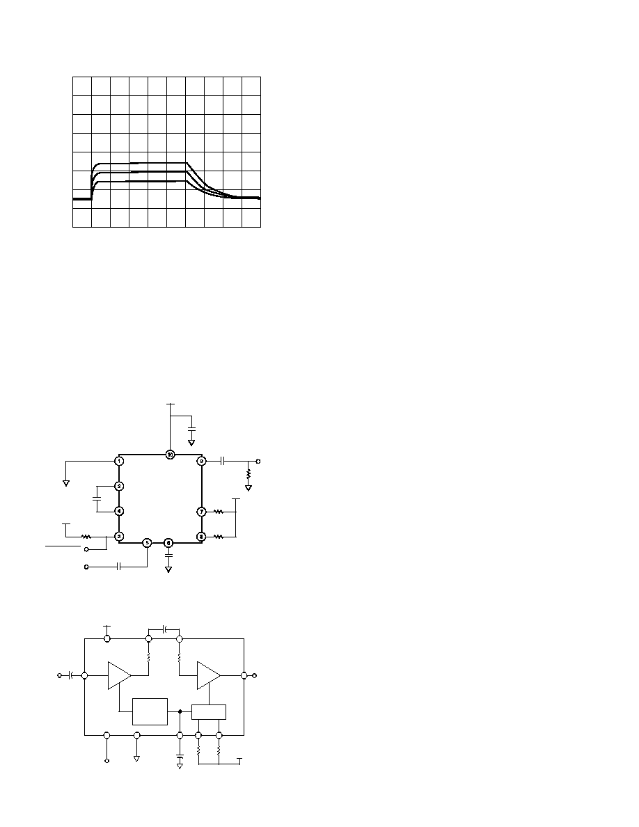
The performance of the rms level detector is illustrated in TPC 12
for a C
AVG
of 2.2
µF and TPC 11 for a C
AVG
of 22
µF. In each of
these photographs, the input signal to the SSM2167 (not shown) is
a series of tone bursts in six successive 10 dB steps. The tone bursts
range from 66 dBV (0.5 mV rms) to 6 dBV (0.5 V rms). As
illustrated in the photographs, the attack time of the rms level
detector is dependent only on C
AVG
, but the release times are linear
ramps whose decay times are dependent on both C
AVG
and the
input signal step size. The rate of release is approximately 240 dB/s
for a C
AVG
of 2.2
µF, and 12 dB/s for a C
AVG
of 22
µF.
Control Circuitry
The output of the rms level detector is a signal proportional to
the log of the true rms value of the buffer output with an added
dc offset. The control circuitry subtracts a dc voltage from this
signal, scales it, and sends the result to the VCA to control the
gain. The VCA's gain control is logarithmic--a linear change in
control signal causes a dB change in gain. It is this control law
that allows linear processing of the log rms signal to provide the
flat compression characteristic on the input/output characteristic
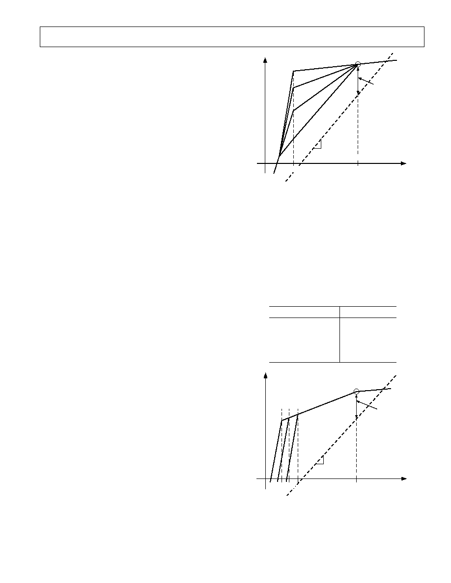
shown in Figure 1.
INPUT dB
OUTPUT
dB
V
DE
V
RP
15:1
5:1
2:1
1:1
1
1
VCA GAIN
Figure 4. Effect of Varying the Compression Ratio
Setting the Compression Ratio
Changing the scaling of the control signal fed to the VCA causes a
change in the circuit's compression ratio, "r." This effect is shown
in Figure 4. Connecting a resistor (R
COMP
) between Pin 8 and V
DD
sets the compression ratio. Lowering R
COMP
gives smaller compres-
sion ratios as indicated in Table I. AGC performance is achieved
with compression ratios between 2:1 and 10:1, and is dependent
on the application. Shorting R
COMP
will disable the AGC function,
setting the compression equal to 1:1. If using a compression resis-
tor, using a value greater than 5 k
is recommend. If lower than
5 k
is used, the device may interpret this as a short, 0 .
Table I. Setting Compression Ratio
Compression Ratio
Value of R
COMP
1:1
0
(short to V+)
2:1
15 k
3:1
35 k
5:1
75 k
10:1
175 k
VCA GAIN
INPUT dB
OUTPUT
dB
V
DE1
V
RP
V
DE3
V
DE2
1
1
r:1
Figure 5. Effects of Varying the Downward Expansion
(Noise Gate) Threshold
REV. A
8
C0262803/02(A)
PRINTED IN U.S.A.
SSM2167
Setting the Noise Gate Threshold (Downward Expansion)
Noise gate threshold is another programmable point using an
external resistor (R
GATE
) that is connected between Pin 7
(NOISE GATE THRS) and V
DD
. The downward expansion
threshold may be set between 40 dBV and 55 dBV, as shown
in Table II. The downward expansion threshold is inversely
proportional to the value of this resistance: setting this resistance
to 0
sets the threshold at approximately 10 mV rms (40 dBV),
whereas a 5 k
resistance sets the threshold at approximately
1 mV rms (55 dBV). This relationship is illustrated in Figure 5.
We do not recommend more than 5 k
for the R
GATE
resistor as
the noise floor of the SSM2167 prevents the noise gate from
being lowered further without causing problems.
Table II. Setting Noise Gate Threshold
Noise Gate (dBV)
Value of R
GATE
40
0
(short to V+)
48
1 k
54
2 k
55
5 k
Rotation Point (Limiting)
Input signals above a particular level, "the rotation point," are
attenuated (limited) by internal circuitry. This feature allows the
SSM2167 to limit the maximum output, preventing clipping of
the following stage, such as a CODEC or ADC. The rotation
point for SSM2167 is set internally to 24 dBV (63 mV rms) for
SSM2167-1 and 20 dBV (100 mV rms) for SSM2167-2.
Shutdown Feature
The supply current of the SSM2167 can be reduced to under 10
µA
by applying an active LOW, 0 V CMOS compatible input to the
SSM2167's /SHUTDOWN Pin (Pin 3). In this state, the input
and output circuitry of the SSM2167 will assume a high imped-
ance state; as such, the potentials at the input pin and the output
pin will be determined by the external circuitry connected to the
SSM2167. The SSM2167 takes approximately 200 ms to settle
from a SHUTDOWN to POWER-ON command. For POWER-ON
to SHUTDOWN, the SSM2167 requires more time, typically less
than 1 s. Cycling the power supply to the SSM2167 can result in
quicker settling times: the off-to-on settling time of the SSM2167 is
less than 200 ms, while the on-to-off settling time is less than 1 ms.
The SSM2167 shutdown current is related to both temperature
and voltage.
PC Board Layout Considerations
Since the SSM2167 is capable of wide bandwidth operation and
can be configured for as much as 60 dB of gain, special care must
be exercised in the layout of the PC board that contains the IC
and its associated components. The following applications hints
should be considered for the PC board.
The layout should minimize possible capacitive feedback from
the output of the SSM2167 back to its input. Do not run input
and output traces adjacent to each other.
A single-point ("star") ground implementation is recommended
in addition to maintaining short lead lengths and PC board runs.
In applications where an analog ground and a digital ground are
available, the SSM2167 and its surrounding circuitry should be
connected to the system's analog ground. As a result of these
recommendations, wire-wrap board connections and grounding
implementations are to be explicitly avoided.
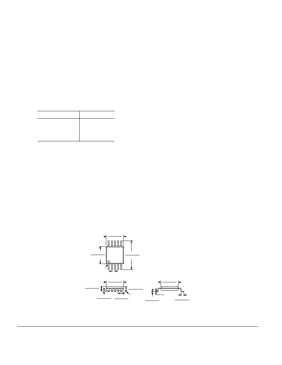
OUTLINE DIMENSIONS
Dimensions shown in inches and (mm).
Revision History
Location
Page
Data Sheet changed from REV. 0 to REV. A.
Edits to Specifications . . . . . . . . . . . . . . . . . . . . . . . . . . . . . . . . . . . . . . . . . . . . . . . . . . . . . . . . . . . . . . . . . . . . . . . . . . . . . . . . . . . . 2
Edits to Figures 2 and 3 . . . . . . . . . . . . . . . . . . . . . . . . . . . . . . . . . . . . . . . . . . . . . . . . . . . . . . . . . . . . . . . . . . . . . . . . . . . . . . . . . . . 6
10-Lead MSOP
(RM-10)
1
10
6
5
0.199 (5.05)
0.187 (4.75)
PIN 1
0.0197 (0.50) BSC
0.124 (3.15)
0.112 (2.84)
0.124 (3.15)
0.112 (2.84)
0.122 (3.10)
0.110 (2.79)
SEATING
PLANE
0.006 (0.15)
0.002 (0.05)
0.016 (0.41)
0.006 (0.15)
0.038 (0.97)
0.030 (0.76)
0.043 (1.09)
0.037 (0.94)
0.011 (0.28)
0.003 (0.08)
0.022 (0.56)
0.021 (0.53)
0.120 (3.05)
0.112 (2.84)
6
0
Document Outline
- Specifications
- Pinout
- Package drawings
- Ordering Guide
- Features
- Applications
- Product Description
- Absolute Maximum Ratings
- Functional Block Diagram
- Circuit Description
- Typical Characteristics
- ESD RATINGS
- CAUTION
- APPLICATIONS INFORMATION
- Revision History
- DIAGRAM
- Typical Application Circuit