Äîêóìåíòàöèÿ è îïèñàíèÿ www.docs.chipfind.ru

2 W Filterless Class-D
Stereo Audio Amplifier
Preliminary Technical Data
SSM2304
Information furnished by Analog Devices is believed to be accurate and reliable. However, no
responsibility is assumed by Analog Devices for its use, nor for any infringements of patents or other
rights of third parties that may result from its use. Specifications subject to change without notice. No
license is granted by implication or otherwise under any patent or patent rights of Analog Devices.
Trademarks and registered trademarks are the property of their respective owners.
One Technology Way, P.O. Box 9106, Norwood, MA 02062-9106, U.S.A.
Tel: 781.329.4700
www.analog.com
Fax: 781.461.3113
©2006 Analog Devices, Inc. All rights reserved.
FEATURES
Filterless Class-D amplifier with built-in output stage
2 W into 4 and 1.2 W into 8 at 5.0 V supply with less than
10% THD
85% efficiency at 5.0 V, 2W into 4 speaker
Better than 95dB SNR (signal-to-noise ratio)
Available in 16-lead 3 mm × 3 mm LFCSP
Single-supply operation from 2.2 V to 5.0 V
20 nA ultralow shutdown current
Short-circuit and thermal protection
Pop-and-click suppression
Built-in resistors reduce board component count
Default fixed 18dB gain and user-adjustable
APPLICATIONS
Notebooks and PCs
Mobile phones
MP3 players
Portable gaming
Portable electronics
Educational toys
GENERAL DESCRIPTION
The SSM2304 is a fully integrated, high efficiency, Class-D stereo
audio amplifier. It is designed to maximize performance for
portable applications. The application circuit requires a
minimum of external components and operates from a single
2.2 V to 5.0 V supply. It is capable of delivering 2 W of con-
tinuous output power with less than 10% THD + N driving a
4 load from a 5.0 V supply.
The SSM2304 features a high efficiency, low noise modulation
scheme. It operates with 85% efficiency at 2 W into 4 from a
5.0 V supply and has a signal-to-noise ratio (SNR) that is better
than 95 dB. PDM modulation is used to provide lower EMI-
radiated emissions compared with other Class-D architectures.
The SSM2304 has a micropower shutdown mode with a typical
shutdown current of 20 nA. Shutdown is enabled by applying a
logic low to the SD pin.
The architecture of the device allows it to achieve a very low level
of pop and click. This minimizes voltage glitches at the output
during turn-on and turn-off, thus reducing audible noise on
activation and deactivation.
The fully differential input of the SSM2304 provides excellent
rejection of common-mode noise on the input. Input coupling
capacitors can be omitted if the dc input common-mode voltage
is approximately V
DD
/2.
The SSM2304 also has excellent rejection of power supply noise,
including noise caused by GSM transmission bursts and RF
rectification. PSRR is typically 70 dB at 217 Hz.
The gain can be set to 6 dB or 18 dB utilizing the gain control
select pin connected respectively to ground or V
DD
. Gain can
also be adjusted externally by using an external resistor.
The SSM2304 is specified over the commercial temperature range
(-40°C to +85°C). It has built-in thermal shutdown and output
short-circuit protection. It is available in a 16-lead, 3 mm × 3 mm
lead-frame chip scale package (LFCSP).
Rev. PrD
SSM2304
Preliminary Technical Data
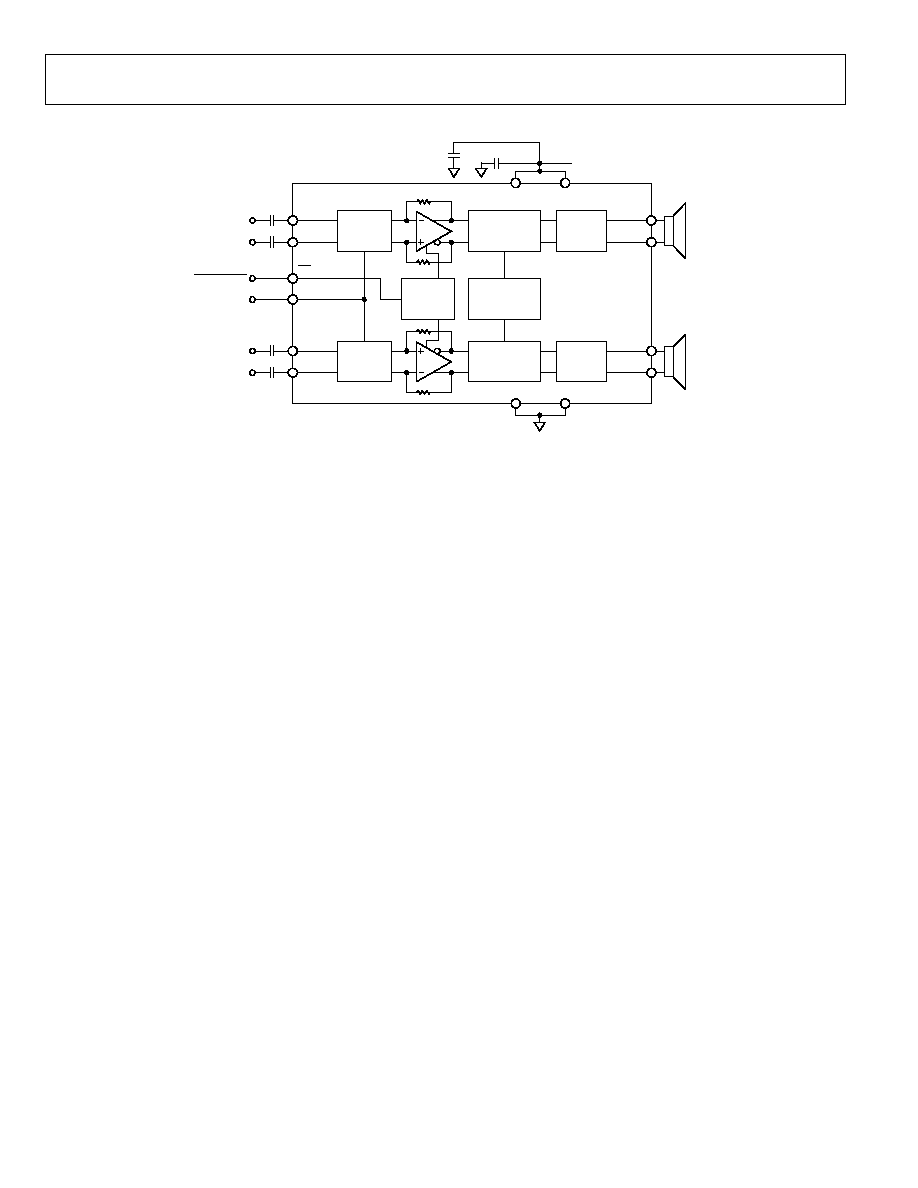
FUNCTIONAL BLOCK DIAGRAM
GAIN
CONTROL
FET
DRIVER
MODULATOR
0.1µF
VDD
VDD
GND
GND
INTERNAL
OSCILLATOR
OUTR+
OUTR
OUTL+
OUTL
GAIN
CONTROL
BIAS
FET
DRIVER
MODULATOR
INR+
VBATT
2.5V TO 5.0V
INR
GAIN
SD
GAIN
SHUTDOWN
INL+
INL
10µF
0.01µF
1
1
INPUT CAPS ARE OPTIONAL IF INPUT DC COMMON-MODE
VOLTAGE IS APPROXIMATELY V
DD
/2.
0.01µF
1
0.01µF
1
0.01µF
1
LEFT IN+
LEFT IN
RIGHT IN
RIGHT IN+
SSM2304
06
16
2-
0
01
Figure 1.
Rev. PrD | Page 2 of 19

Preliminary Technical Data
SSM2304
TABLE OF CONTENTS
Features...............................................................................................1
Applications .......................................................................................1
General Description..........................................................................1
Functional Block Diagram ...............................................................2
Revision History ................................................................................3
Specifications .....................................................................................4
Absolute Maximum Ratings ............................................................5
Thermal Resistance.......................................................................5
ESD Caution ..................................................................................5
Pin Configuration and Function Descriptions .............................6
Typical Performance Characteristics ..............................................7
Typical Application Circuits ..........................................................11
Application Notes............................................................................12
Overview ......................................................................................12
Gain Selection..............................................................................12
Pop-and-Click Suppression .......................................................12
EMI Noise ....................................................................................12
Layout ...........................................................................................13
Input Capacitor Selection ..........................................................13
Proper Power Supply Decoupling.............................................13
Evaluation Board Information ......................................................14
Introduction.................................................................................14
Operation .....................................................................................14
SSM2304 Application Board Schematic ..................................15
SSM2304 Stereo Class-D Amplifier Evaluation Module
Component List...........................................................................16
SSM2304 Application Board Layout ........................................17
Outline Dimensions........................................................................18
Ordering Guide ...........................................................................18
REVISION HISTORY
7/06--Revision 0: Initial Version
Rev. PrD | Page 3 of 19
SSM2304
Preliminary Technical Data
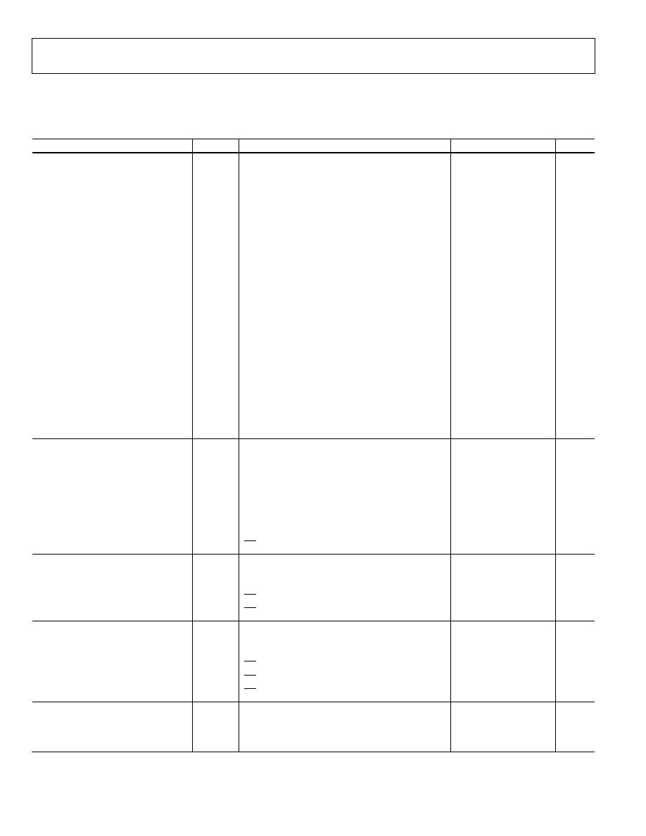
SPECIFICATIONS
V
DD
= 5.0 V, T
A
= 25
o
C, R
L
= 8 , Gain=6dB, unless otherwise noted
Table 1.
Parameter Symbol
Conditions
Min
Typ
Max
Unit
DEVICE CHARACTERISTICS
Output Power
P
O
R
L
= 4 , THD = 1%, f = 1 kHz, 20 kHz BW, V
DD
= 5.0 V
W
R
L
= 8 , THD = 1%, f = 1 kHz, 20 kHz BW, V
DD
= 5.0 V
1.4
W
R
L
= 4 , THD = 1%, f = 1 kHz, 20 kHz BW, V
DD
= 3.6 V
TBD
W
R
L
= 8 , THD = 1%, f = 1 kHz, 20 kHz BW, V
DD
= 3.6 V
0.615
W
R
L
= 4 , THD = 1%, f = 1 kHz, 20 kHz BW, V
DD
= 2.5 V
TBD
W
R
L
= 8 , THD = 1%, f = 1 kHz, 20 kHz BW, V
DD
= 2.5 V
0.275
W
R
L
= 4 , THD = 10%, f = 1 kHz, 20 kHz BW, V
DD
= 5.0 V
3.3
W
R
L
= 8 , THD = 10%, f = 1 kHz, 20 kHz BW, V
DD
= 5.0 V
1.53
W
R
L
= 4 , THD = 10%, f = 1 kHz, 20 kHz BW, V
DD
= 3.6 V
TBD
W
R
L
= 8 , THD = 10%, f = 1 kHz, 20 kHz BW, V
DD
= 3.6 V
0.77
W
R
L
= 4 , THD = 10%, f = 1 kHz, 20 kHz BW, V
DD
= 2.5 V
TBD
W
R
L
= 8 , THD = 10%, f = 1 kHz, 20 kHz BW, V
DD
= 2.5 V
0.35
W
Efficiency
P
OUT
= 2.5 W, 4 , V
DD
= 5.0 V
87
%
P
OUT
= 1.4 W, 8 , V
DD
= 5.0 V
85
%
Total Harmonic Distortion + Noise
THD + N
P
O
= 2 W into 4 each channel, f = 1 kHz, V
DD
= 5.0 V
0.2
%
P
O
= 1 W into 8 each channel, f = 1 kHz, V
DD
= 3.6 V
0.25
%
Input Common-Mode Voltage Range
V
CM
1.0
V
DD
- 1
V
Common-Mode Rejection Ratio
CMRR
GSM
V
CM
= 2.5 V ± 100 mV at 217 Hz
60
dB
Channel Separation
X
TALK
P
O
= 100 mW
, f = 1 kHz
78
dB
Average Switching Frequency
f
SW
1.8
MHz
Differential Output Offset Voltage
V
OOS
G = 6 dB
2.0
mV
POWER SUPPLY
Supply Voltage Range
V
DD
Guaranteed from PSRR test
2.5
5.0
V
Power Supply Rejection Ratio
PSRR
V
DD
= 2.5 V to 5.0 V , 50 Hz, input floating/ground
70
85
dB
PSRR
GSM
V
RIPPLE
= 100 mV rms at 217 Hz, inputs ac GND,
C
IN
= 0.01 F, input referred
70
dB
Supply Current
I
SY
V
IN
= 0 V, no load, V
DD
= 5.0 V
7.0
mA
V
IN
= 0 V, no load, V
DD
= 3.6 V
6.5
mA
V
IN
= 0 V, no load, V
DD
= 2.5 V
5.2
mA
Shutdown Current
I
SD
SD = GND
20
nA
GAIN CONTROL
Closed-Loop Gain
Av0
GAIN1 = 0 V
6
dB
Av1
GAIN2
=
V
DD
12
dB
Differential Input Impedance
Z
IN
SD = VDD, Av0 and Av1 modes
37.5
K
SD = GND
210
K
SHUTDOWN CONTROL
Input Voltage High
V
IH
I
SY
1 mA
1.2
V
Input Voltage Low
V
IL
I
SY
300 nA
0.5
V
Turn-On Time
t
WU
SD rising edge from GND to V
DD
30
ms
Turn-Off Time
t
SD
SD falling edge from V
DD
to GND
5
s
Output Impedance
Z
OUT
SD = GND
>100
K
NOISE PERFORMANCE
Output Voltage Noise
e
n
V
DD
= 3.6 V, f = 20 Hz to 20 kHz, inputs are ac
grounded, A
V
= 6 dB, A weighting
35
V
Signal-to-Noise Ratio
SNR
P
OUT
= 2.5 W, R
L
= 4
98
dB
Rev. PrD | Page 4 of 19
Preliminary Technical Data
SSM2304
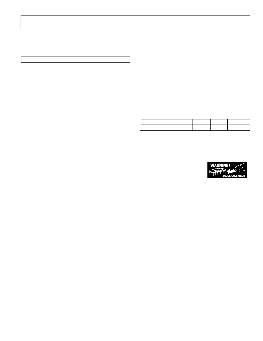
ABSOLUTE MAXIMUM RATINGS
Absolute maximum ratings apply at 25°C, unless otherwise noted.
Table 2.
Parameter Rating
Supply Voltage
6 V
Input Voltage
V
DD
Common-Mode Input Voltage
V
DD
ESD Susceptibility
4 kV
Storage Temperature Range
-65°C to +150°C
Operating Temperature Range
-40°C to +85°C
Junction Temperature Range
-65°C to +165°C
Lead Temperature Range
(Soldering, 60 sec)
300°C
Stresses above those listed under Absolute Maximum Ratings
may cause permanent damage to the device. This is a stress
rating only; functional operation of the device at these or any
other conditions above those indicated in the operational
section of this specification is not implied. Exposure to absolute
maximum rating conditions for extended periods may affect
device reliability.
THERMAL RESISTANCE
JA
is specified for the worst-case conditions, that is, a device
soldered in a circuit board for surface-mount packages.
Table 3. Thermal Resistance
Package Type
JA
JC
Unit
16-lead, 3 mm × 3 mm LFCSP
44
31.5
°C/W
ESD CAUTION
ESD (electrostatic discharge) sensitive device. Electrostatic charges as high as 4000 V readily accumulate on
the human body and test equipment and can discharge without detection. Although this product features
proprietary ESD protection circuitry, permanent damage may occur on devices subjected to high energy
electrostatic discharges. Therefore, proper ESD precautions are recommended to avoid performance
degradation or loss of functionality.
Rev. PrD | Page 5 of 19
SSM2304
Preliminary Technical Data
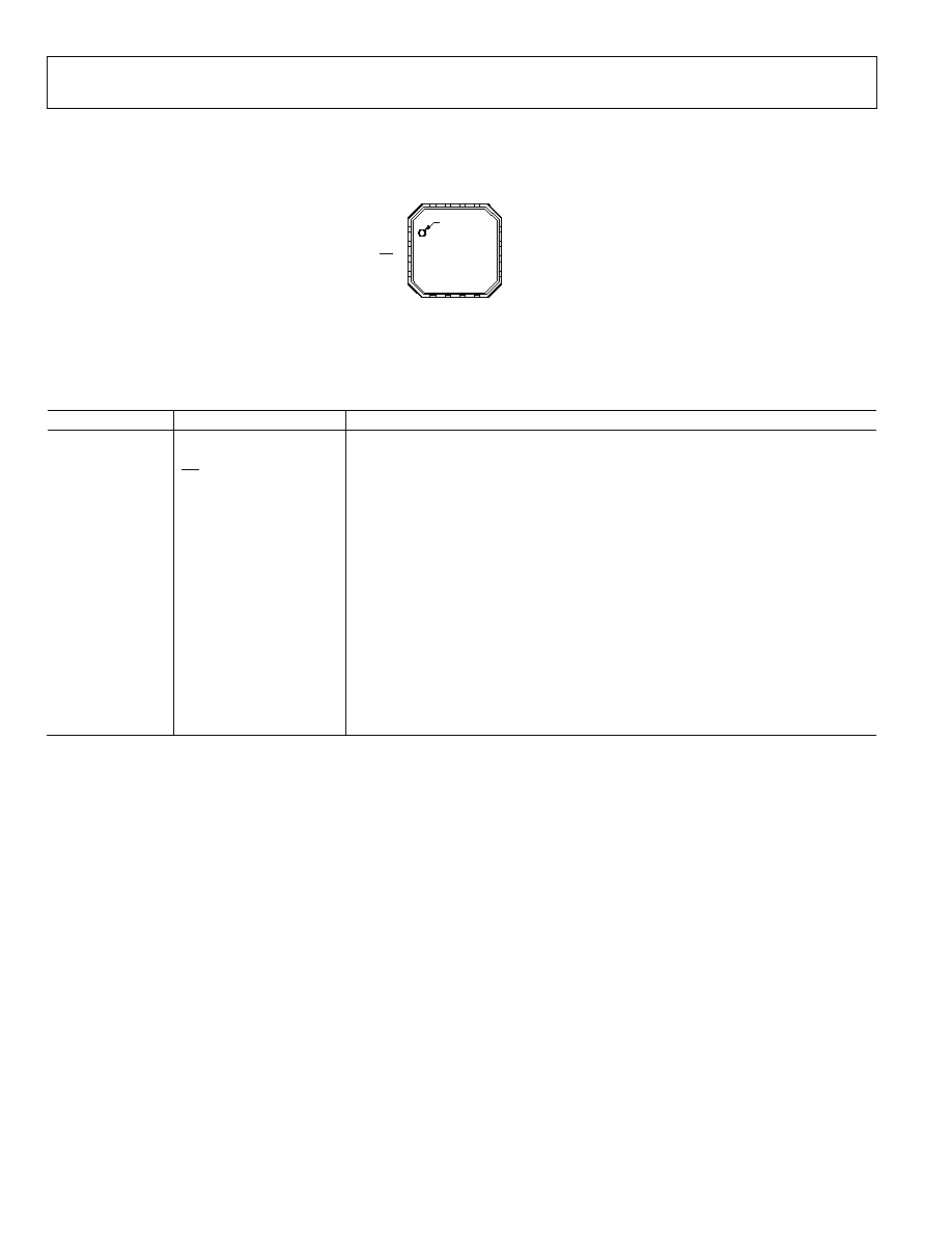
PIN CONFIGURATION AND FUNCTION DESCRIPTIONS
PIN 1
INDICATOR
NC = NO CONNECT
1
OUTL+
2
OUTL
3
SD
4
INL+
11 OUTR
12 OUTR+
10 GAIN
9 INR+
5
I
N
L
6
N
C
7
N
C
8
I
N
R
1
5
V
D
D
1
6
G
N
D
1
4
V
D
D
1
3
G
N
D
TOP VIEW
(Not to Scale)
SSM2304
0
61
62
-
00
2
Figure 2. SSM2304 LFCSP Pin Configuration
Table 4. Pin Function Descriptions
Pin No.
Mnemonic
Description
1
OUTL+
Inverting Output for Left Channel.
2
OUTL-
Noninverting Output for Left Channel.
3
SD
Shutdown Input. Active low digital input.
4
INL+
Noninverting Input for Left Channel.
5
INL-
Inverting Input for Left Channel.
6 NC
No
Connect.
7 NC
No
Connect.
8
INR-
Inverting Input for Right Channel.
9
INR+
Noninverting Input for Right Channel.
10
GAIN
Gain Selection. Digital input.
11
OUTR-
Noninverting Output for Right Channel.
12 OUTR+
Inverting Output for Right Channel.
13
GND
Ground for Output Amplifiers.
14
VDD
Power Supply for Output Amplifiers.
15
VDD
Power Supply for Output Amplifiers.
16
GND
Ground for Output Amplifiers.
Rev. PrD | Page 6 of 19
Preliminary Technical Data
SSM2304
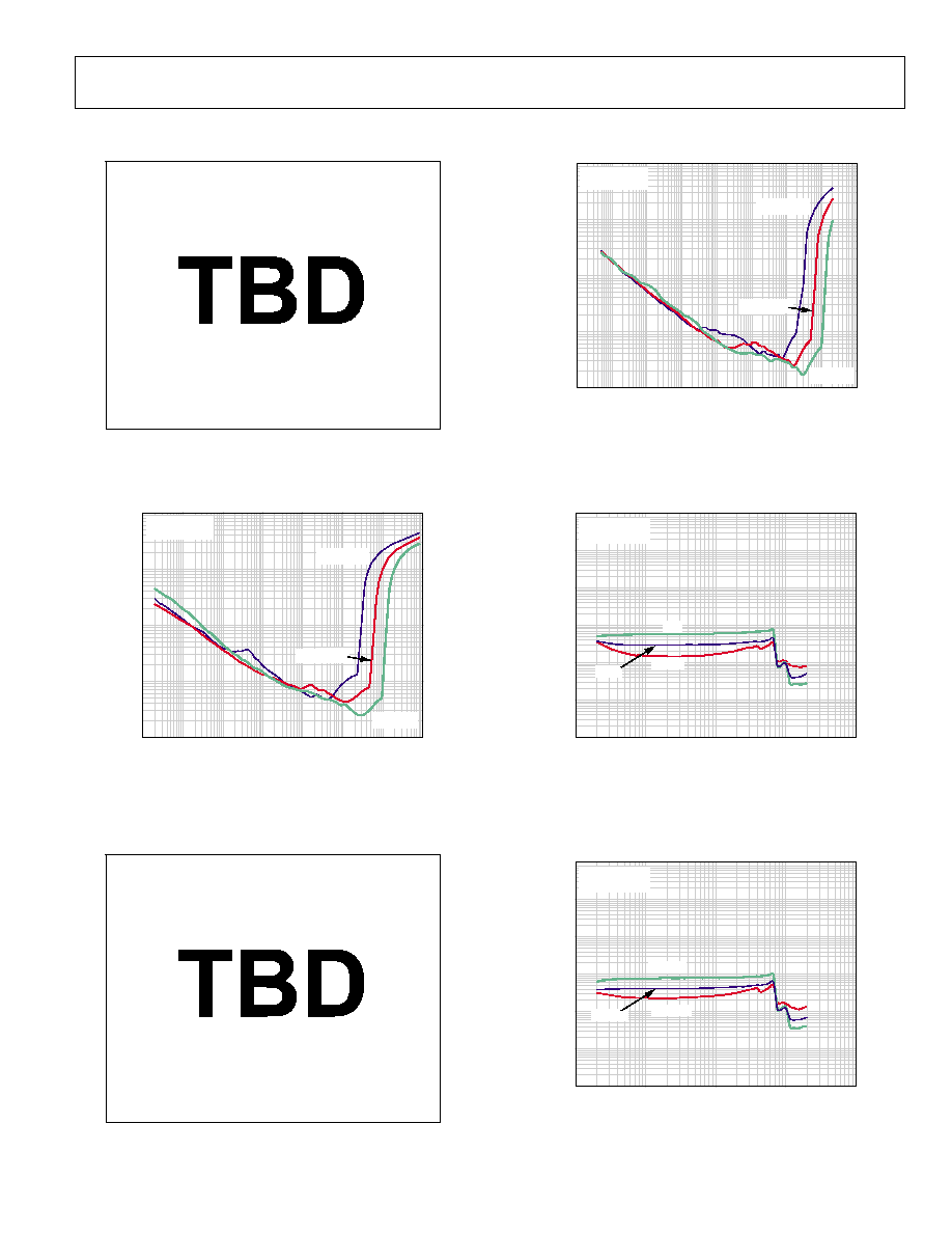
TYPICAL PERFORMANCE CHARACTERISTICS
Figure 3. THD + N vs. Output Power into 4 , A
V
= 12 dB
100
0.01
0.000001
0.0001
0.00001
10
OUTPUT POWER (W)
T
HD +
N (
%
)
10
1
0.1
0.001
0.01
0.1
1
R
L
= 8, 33µH
GAIN = 12dB
V
DD
= 2.5V
V
DD
= 3.6V
V
DD
= 5V
06
16
2-
00
3
Figure 4. THD + N vs. Output Power into 8 , A
V
= 12 dB
Figure 5. THD + N vs. Output Power into 4 , A
V
= 6 dB
100
0.01
0.0000001
0.000001
0.0001
0.00001
10
OUTPUT POWER (W)
T
HD +
N
(
%
)
10
1
0.1
0.001
0.01
0.1
1
R
L
= 8, 33µH
GAIN = 6dB
V
DD
= 2.5V
V
DD
= 3.6V
V
DD
= 5V
06
16
2-
00
4
Figure 6. THD + N vs. Output Power into 8 , A
V
= 6 dB
100
0.0001
10
100k
FREQUENCY (Hz)
T
HD +
N (
%
)
V
DD
= 5V
R
L
= 8, 33µH
0.5W
0.25W
1W
10
1
0.1
0.01
0.001
100
1k
10k
06
16
2-
00
5
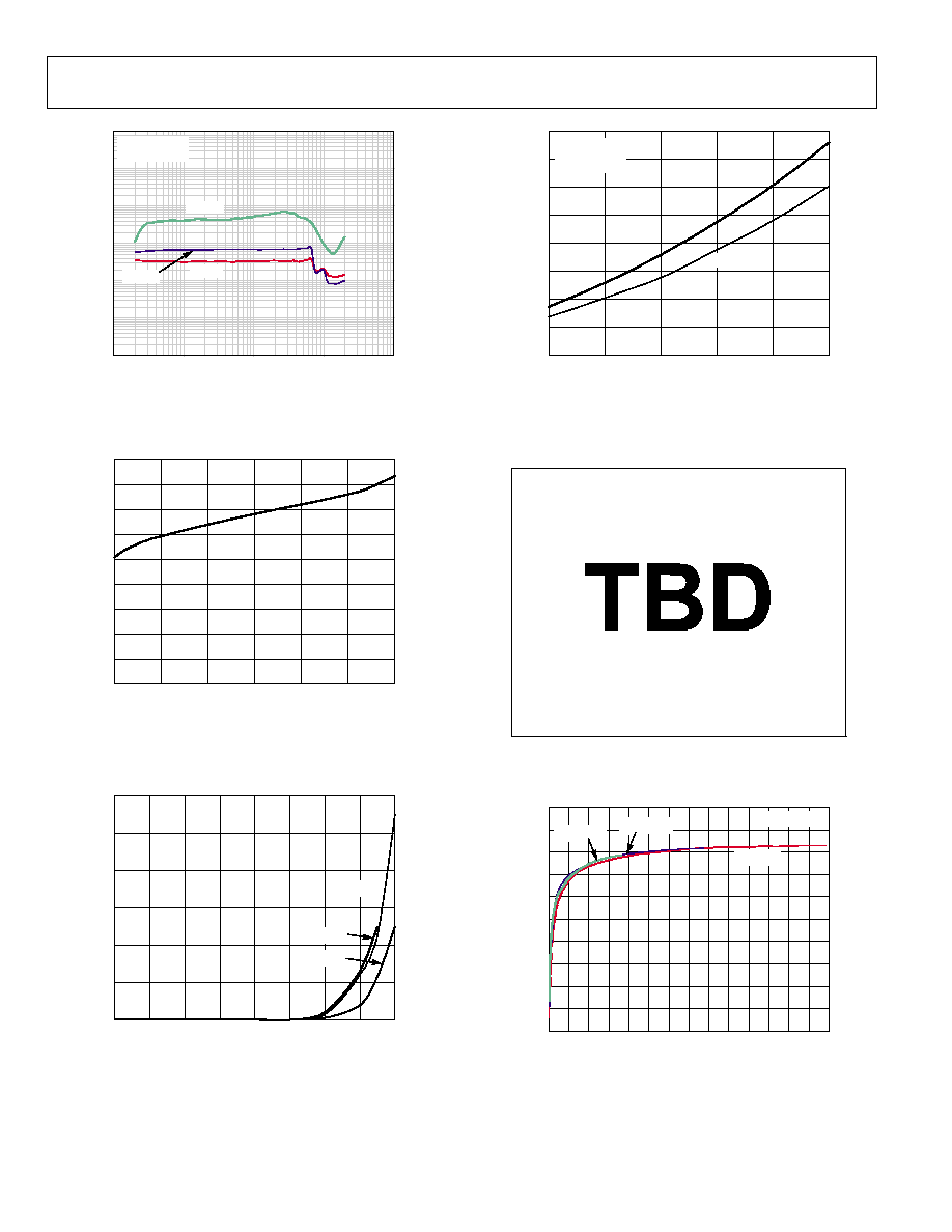
Figure 7. THD + N vs. Frequency, V
DD
= 5.0 V
100
0.0001
10
100k
FREQUENCY (Hz)
T
HD +
N (
%
)
V
DD
= 3.6V
R
L
= 8, 33µH
250mW
125mW
500mW
10
1
0.1
0.01
0.001
100
1k
10k
06
16
2-
00
6
Figure 8. THD + N vs. Frequency, V
DD
= 3.6 V
Rev. PrD | Page 7 of 19
SSM2304
Preliminary Technical Data
100
0.0001
10
100k
FREQUENCY (Hz)
T
HD +
N (
%
)
V
DD
= 2.5V
R
L
= 8, 33µH
125mW
75mW
250mW
10
1
0.1
0.01
0.001
100
1k
10k
06
16
2-
00
7
Figure 9. THD + N vs. Frequency, V
DD
= 2.5 V
9
0
2.5
5.5
SUPPLY VOLTAGE (V)
S
UP
P
L
Y
CURR
E
NT
(
m
A)
8
7
6
5
4
3
2
1
3.0
3.5
4.0
4.5
5.0
06
16
2-
00
8
Figure 10. Supply Current vs. Supply Voltage, No Load
12
0
0
0.8
SHUTDOWN VOLTAGE (V)
S
HUT
DO
W
N CUR
RE
NT
(
µ
A)
10
8
6
4
2
0.1
0.2
0.3
0.4
0.5
0.6
0.7
V
DD
= 2.5V
V
DD
= 3.6V
V
DD
= 5V
06
16
2-
00
9
Figure 11. Supply Current vs. Shutdown Voltage
1.6
0
2.5
5.0
SUPPLY VOLTAGE (V)
O
UT
P
UT
P
O
W
E
R (
W
)
10%
1%
1.4
1.2
1.0
0.8
0.6
0.4
0.2
3.0
3.5
4.0
4.5
f
= 1kHz
GAIN = 2
R
L
= 8, 33µH
06
16
2-
01
0
Figure 12. Maximum Output Power vs. Supply Voltage
Figure 13. Efficiency vs. Output Power into 4
100
0
0
1.4
OUTPUT POWER (W)
EF
F
I
C
I
EN
C
Y
(%
)
R
L
= 8, 33µH
90
80
70
60
50
40
30
20
10
0.1 0.2 0.3 0.4 0.5 0.6 0.7 0.8 0.9 1.0 1.1 1.2 1.3
V
DD
= 2.5V
V
DD
= 3.6V
V
DD
= 5V
06
16
2-
01
1
Figure 14. Efficiency vs. Output Power into 8
Rev. PrD | Page 8 of 19
Preliminary Technical Data
SSM2304
1.0
0
0
0.8
OUTPUT POWER (W)
P
O
W
E
R DI
S
S
I
P
AT
I
O
N
(
W
)
V
DD
= 3.6V
R
L
= 8, 33µH
0.9
0.8
0.7
0.6
0.5
0.4
0.3
0.2
0.1
0.1
0.2
0.3
0.4
0.5
0.6
0.7
06
16
2-
01
2
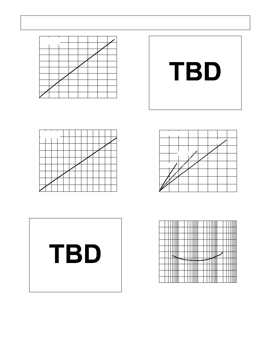
Figure 15. Power Dissipation vs. Output Power at V
DD
= 3.6 V
1.8
0
0
1.3
OUTPUT POWER (W)
P
O
W
E
R DI
S
S
I
P
AT
I
O
N
(
W
)
V
DD
= 5V
R
L
= 8, 33µH
1.6
1.4
1.2
1.0
0.8
0.6
0.4
0.2
0.1 0.2 0.3 0.4 0.5 0.6 0.7 0.8 0.9 1.0 1.1 1.2
06
16
2-
01
3
Figure 16. Power Dissipation vs. Output Power at V
DD
= 5.0 V
Figure 17. Output Power vs. Load Resistance, THD = 10%
Figure 18. Output Power vs. Load Resistance, THD = 1%
400
0
0
1.6
OUTPUT POWER (W)
S
UP
P
L
Y
CURR
E
NT
(
m
A)
V
DD
= 2.5V
V
DD
= 3.6V
V
DD
= 5V
350
300
250
200
150
100
50
0.2
0.4
0.6
0.8
1.0
1.2
1.4
R
L
= 8, 33µH
06
16
2-
01
4
Figure 19. Output Power vs. Supply Current, One Channel
0
100
10
100k
FREQUENCY (Hz)
P
S
RR (
d
B)
10
20
30
40
50
60
70
80
90
100
1k
10k
06
16
2-
0
15
Figure 20. Power Supply Rejection Ratio vs. Frequency
Rev. PrD | Page 9 of 19
SSM2304
Preliminary Technical Data
0
80
10
100k
FREQUENCY (Hz)
CM
R
R (
d
B)
100
1k
10k
10
20
30
40
50
60
70
R
L
= 8, 33µH
GAIN = 6dB
06
16
2-
01
6
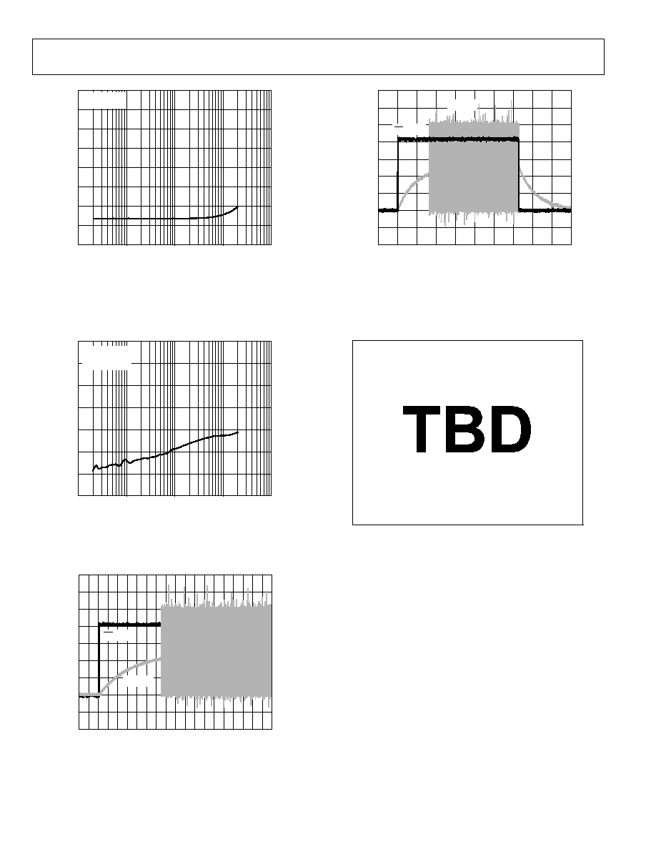
Figure 21. Common-Mode Rejection Ratio vs. Frequency
0
140
10
100k
FREQUENCY (Hz)
CRO
S
S
T
AL
K (
d
B)
100
1k
10k
20
40
60
80
100
120
V
DD
= 3.6V
V
RIPPLE
= 1V rms
R
L
= 8, 33µH
06
16
2-
01
7
Figure 22. Crosstalk vs. Frequency
7
2
10
90
TIME (ms)
VO
L
T
A
G
E
6
5
4
3
2
1
0
1
5 0 5 10 15 20 25 30 35 40 45 50 55 60 65 70 75 80 85
SD INPUT
OUTPUT
06
16
2-
01
8
Figure 23. Turn-On Response
7
2
20
180
TIME (ms)
VO
L
T
A
G
E
6
5
4
3
2
1
0
1
0
20
40
60
80
100
120
140
160
SD INPUT
OUTPUT
06
16
2-
01
9
Figure 24. Turn-Off Response
Figure 25. Output Frequency Spectrum
Rev. PrD | Page 10 of 19
Preliminary Technical Data
SSM2304
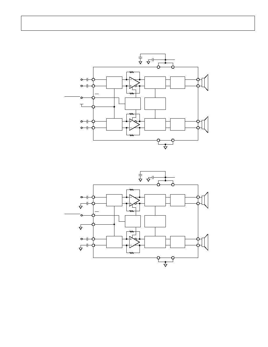
TYPICAL APPLICATION CIRCUITS
GAIN
CONTROL
FET
DRIVER
MODULATOR
VDD
VDD
GND
GND
V
DD
INTERNAL
OSCILLATOR
OUTR+
OUTR
OUTL+
OUTL
GAIN
CONTROL
BIAS
FET
DRIVER
MODULATOR
INR+
INR
GAIN
SD
GAIN
SHUTDOWN
INL+
INL
0.01µF
1
1
INPUT CAPS ARE OPTIONAL IF INPUT DC COMMON-MODE
VOLTAGE IS APPROXIMATELY V
DD
/2.
0.01µF
1
0.01µF
1
0.01µF
1
LEFT IN+
LEFT IN
RIGHT IN
RIGHT IN+
SSM2304
0.1µF
VBATT
2.5V TO 5.0V
10µF
06
16
2-
03
0
Figure 26. Stereo Differential Input Configuration
GAIN
CONTROL
FET
DRIVER
MODULATOR
VDD
VDD
GND
GND
INTERNAL
OSCILLATOR
OUTR+
OUTR
OUTL+
OUTL
GAIN
CONTROL
BIAS
FET
DRIVER
MODULATOR
INR+
INR
SD
SHUTDOWN
INL+
INL
0.01µF
0.01µF
0.01µF
0.01µF
LEFT IN
RIGHT IN
SSM2304
GAIN
GAIN
0.1µF
VBATT
2.5V TO 5.0V
10µF
06
16
2-
03
1
Figure 27. Stereo Single-Ended Input Configuration
Rev. PrD | Page 11 of 19
SSM2304
Preliminary Technical Data
APPLICATION NOTES
OVERVIEW
The SSM2304 stereo Class-D audio amplifier features a filterless
modulation scheme that greatly reduces the external components
count, conserving board space and thus reducing systems cost.
The SSM2304 does not require an output filter, but instead relies
on the inherent inductance of the speaker coil and the natural
filtering of the speaker and human ear to fully recover the audio
component of the square-wave output. While most Class-D ampli-
fiers use some variation of pulse-width modulation (PWM), the
SSM2304 uses a - modulation to determine the switching
pattern of the output devices. This provides a number of important
benefits. - modulators do not produces a sharp peak with
many harmonics in the AM frequency band, as pulse-width
modulators often do. - modulation provides the benefits of
reducing the amplitude of spectral components at high frequencies;
that is, reducing EMI emission that might otherwise be radiated
by speakers and long cable traces. The SSM2304 also offers
protection circuits for overcurrent and temperature protection.
GAIN SELECTION
The SSM2304 has a pair of internal resistors which set a 18dB of
default gain of the amplifier.
It is possible to adjust the SSM2304 gain by using external resistors
at the input. To set a gain lower than 18 dB refer to Error!
Reference source not found.
for differential input
configuration and Error! Reference source not found. for
single-ended configuration. The external gain configuration is
calculated as
External Gain Settings = 300k/(37.5k+Rext)
The gain pin is not connected internally, therefore its external
connection is not required.
POP-AND-CLICK SUPPRESSION
Voltage transients at the output of audio amplifiers can occur when
shutdown is activated or deactivated. Voltage transients as low
as 10 mV can be heard as an audio pop in the speaker. Clicks
and pops can also be classified as undesirable audible transients
generated by the amplifier system, therefore as not coming from
the system input signal. Such transients can be generated when
the amplifier system changes its operating mode. For example, the
following can be sources of audible transients: system power-up/
power-down, mute/unmute, input source change, and sample rate
change. The SSM2304 has a pop-and-click suppression architecture
that reduces this output transients, resulting in noiseless activation
and deactivation.
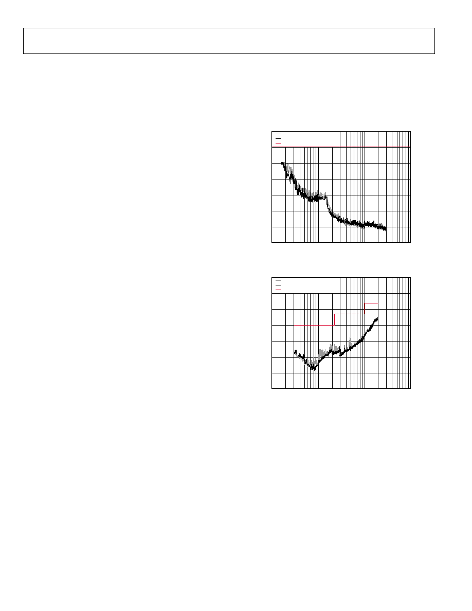
EMI NOISE
The SSM2304 uses a proprietary modulation and spread-
spectrum technology to minimize EMI emissions from the
device. Figure 28 shows SSM2304 EMI emission starting from
100 kHz to 30 MHz. Figure 29 shows SSM2304 EMI emission
from 30 kHz to 2 GHz. These figures clearly describe the SSM2304
EMI behavior as being well below the FCC regulation values,
starting from 100 kHz and passing beyond 1 GHz of frequency.
Although the overall EMI noise floor is slightly higher, frequency
spurs from the SSM2304 are greatly reduced.
70
0
0.1
100
FREQUENCY (MHz)
L
E
V
E
L
(d
B
(µ
V
/
m
))
60
50
40
30
20
10
1
10
= HORIZONTAL
= VERTICAL
= REGULATION VALUE
06
16
2-
03
2
Figure 28. EMI Emissions from SSM2304
70
0
10
10k
FREQUENCY (MHz)
L
E
V
E
L
(d
B
(µ
V
/
m
))
60
50
40
30
20
10
100
1k
= HORIZONTAL
= VERTICAL
= REGULATION VALUE
06
16
2-
03
3
Figure 29. EMI Emissions from SSM2304
The measurements for Figure 28 and Figure 29 were taken with
a 1 kHz input signal, producing 0.5 W output power into an 8
load from a 3.6 V supply. Cable length was approximately 5 cm.
The EMI was detected using a magnetic probe touching the 2"
output trace to the load.
Rev. PrD | Page 12 of 19

Preliminary Technical Data
SSM2304
LAYOUT
As output power continues to increase, care needs to be taken to
lay out PCB traces and wires properly between the amplifier,
load, and power supply. A good practice is to use short, wide
PCB tracks to decrease voltage drops and minimize inductance.
Make track widths at least 200 mil for every inch of track length
for lowest DCR, and use 1 oz or 2 oz of copper PCB traces to
further reduce IR drops and inductance. A poor layout
increases voltage drops, consequently affecting efficiency. Use
large traces for the power supply inputs and amplifier outputs to
minimize losses due to parasitic trace resistance. Proper
grounding guidelines helps to improve audio performance,
minimize crosstalk between channels, and prevent switching
noise from coupling into the audio signal. To maintain high
output swing and high peak output power, the PCB traces that
connect the output pins to the load and supply pins should be as
wide as possible to maintain the minimum trace resistances. It
is also recommended to use a large-area ground plane for
minimum impedances. Good PCB layouts also isolate critical
analog paths from sources of high interference. High frequency
circuits (analog and digital) should be separated from low
frequency ones. Properly designed multilayer printed circuit
boards can reduce EMI emission and increase immunity to RF
field by a factor of 10 or more compared with double-sided
boards. A multilayer board allows a complete layer to be used
for ground plane, whereas the ground plane side of a double-
side board is often disrupted with signal crossover. If the system
has separate analog and digital ground and power planes, the
analog ground plane should be underneath the analog power
plane, and, similarly, the digital ground plane should be
underneath the digital power plane. There should be no overlap
between analog and digital ground planes nor analog and
digital power planes.
INPUT CAPACITOR SELECTION
The SSM2304 will not require input coupling capacitors if the
input signal is biased from 1.0 V to V
DD
- 1.0 V. Input
capacitors are required if the input signal is not biased within
this recommended input dc common-mode voltage range, if
high-pass filtering is needed (Figure 26), or if using a single-
ended source (Figure 27). If high-pass filtering is needed at the
input, the input capacitor along with the input resistor of the
SSM2304 will form a high-pass filter whose corner frequency is
determined by the following equation:
f
C
= 1/(2 × R
IN
× C
IN
)
Input capacitor can have very important effects on the circuit
performance. Not using input capacitors degrades the output
offset of the amplifier as well as the PSRR performance.
PROPER POWER SUPPLY DECOUPLING
To ensure high efficiency, low total harmonic distortion (THD),
and high PSRR, proper power supply decoupling is necessary.
Noise transients on the power supply lines are short-duration
voltage spikes. Although the actual switching frequency can
range from 10 kHz to 100 kHz, these spikes can contain
frequency components that extend into the hundreds of
megahertz. The power supply input needs to be decoupled with
a good quality low ESL and low ESR capacitor--usually around
4.7 F. This capacitor bypasses low frequency noises to the
ground plane. For high frequency transients noises, use a 0.1 F
capacitor as close as possible to the VDD pin of the device.
Placing the decoupling capacitor as close as possible to the
SSM2304 helps maintain efficiency performance.
Rev. PrD | Page 13 of 19
SSM2304
Preliminary Technical Data
EVALUATION BOARD INFORMATION
INTRODUCTION
The SSM2304 audio power amplifier is a complete low power,
Class-D, stereo audio amplifier capable of delivering 2.8 W/channel
into 4 load. In addition to the minimal parts required for the
application circuit, measurement filters are provided on the
evaluation board so that conventional audio measurements can
be made without additional components.
This section provides an overview of Analog Devices SSM2304
evaluation board. It includes a brief description of the board as
well as a list of the board specifications.
Table 5. SSM2304 Evaluation Board Specifications
Parameter Specification
Supply Voltage Range, V
DD
2.5 V to 5.0 V
Power Supply Current Rating
1.5 A
Continuous Output Power, P
O
(R
L
= 4 , f = 1 kHz, 22 kHz BW)
2 W
Minimum Load Impedance
4
OPERATION
Use the following steps when operating the SSM2304
evaluation board.
Power and Ground
1.
Set the power supply voltage between 2.5 V and 5.0 V. When
connecting the power supply to the SSM2304 evaluation
board, make sure to attach the ground connection to the
GND header pin first and then connect the positive supply
to the VDD header pin.
Inputs and Outputs
1.
Ensure that the audio source is set to the minimum level.
2.
Connect the audio source to Inputs INL± and INR±.
3.
Connect the speakers to Outputs OUTL± and OUTR±.
External Gain Settings
It is possible to adjust the SSM2304 gain lower than 18 dB using
external resistors at the input, refer to Error! Reference source
not found.
6 and Error! Reference source not found.7 on the
product data sheet for proper circuit configuration. For external
gain configuration, use the following formula:
External Gain Settings = 300k/(37.5k+Rext)
Shutdown Control
The shutdown select header controls the shutdown function of
the SSM2304. The shutdown pin on the SSM2304 is active low,
meaning that a low voltage (GND) on this pin places the SSM2304
into shutdown mode.
1.
Select jumper to 1-2 position. Shutdown pulled to V
DD
.
2.
Select jumper to 2-3 position. Shutdown pulled to GND.
Input Configurations
1.
For differential input configuration with input capacitors
do not place a jumper on JP8, JP9, JP10, and JP11.
2.
For differential input configuration without input capacitors
place a jumper on JP8, JP9, JP10, and JP11.
Rev. PrD | Page 14 of 19
Preliminary Technical Data
SSM2304
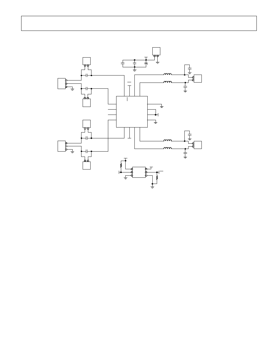
SSM2304 APPLICATION BOARD SCHEMATIC
NC
NC
U1
SSM2302
INR
I
NR+
GA
IN
OU
TR
+
OU
TR
4
3
2
1
IN
L
+
SD
OU
T
L
+
OU
TL
INL
15
14
13
16
GAIN
C4
1nF
C3
1nF
1
2
2
C10
0.01µF
C7
0.1µF
C6
0.1µF
C5
10µF
C11
0.01µF
R3
100k
RIGHT IN
RIN+
RIN
JP11
HEADER 2
JP10
HEADER 2
1
1
2
3
1 2
9
10
11
12
VDD
VDD
V
DD
GND
GND
6
7
8
5
GAIN
SD
L1
FERRITE BEAD
L2
FERRITE BEAD
L1
FERRITE BEAD
OUT RIGHT
OUT LEFT
L2
FERRITE BEAD
SD
C2
1nF
C1
1nF
1
2
V
DD
V
DD
V
DD
HEADER 13C
JP12
6
4
2
5
3
1
2
C8
0.01µF
C9
0.01µF
LEFT IN
JP1
JP3
LIN+
INL+
LIN
JP9
HEADER 2
JP8
HEADER 2
1
1
2
3
1 2
JP2
POWER
1 2
R4
100k
06
16
2-
0
34
Figure 30. SSM2304 Application Board Schematic
Rev. PrD | Page 15 of 19
SSM2304
Preliminary Technical Data
SSM2304 STEREO CLASS-D AMPLIFIER EVALUATION MODULE COMPONENT LIST
Table 6.
Reference
Description
Footprint
Quantity
Manufacturer/Part Number
C8, C9, C10, C11
Capacitors, 0.01 F
0402
4
Murata Manufacturing Co., Ltd./GRM15
C6, C7
Capacitor, 0.1 F
0603
2
Murata Manufacturing Co., Ltd./GRM18
C5
Capacitor, 10 F
0805
1
Murata Manufacturing Co., Ltd./GRM21
C1, C2, C3, C4
Capacitor, 1 nF
0402
4
Murata Manufacturing Co., Ltd./GRM15
R3, R4
Resistor, 100 k
0603
2
Vishay/CRCW06031003F
L1, L2, L3, L4
Ferrite bead
0402
4
Murata Manufacturing Co., Ltd./BLM15EG121
U1
IC, SSM2304
3.0 mm × 3.0 mm
1
SSM2304CSPZ
EVAL BOARD
PCB evaluation board
1
Rev. PrD | Page 16 of 19
Preliminary Technical Data
SSM2304
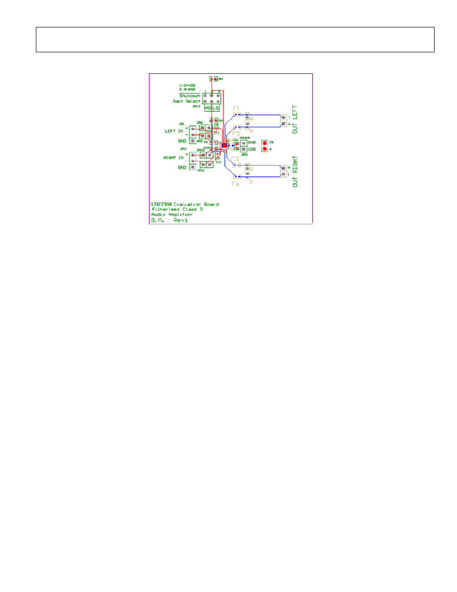
SSM2304 APPLICATION BOARD LAYOUT
06
16
2-
0
35
Figure 31. SSM2304 Application Board Layout
Rev. PrD | Page 17 of 19
SSM2304
Preliminary Technical Data
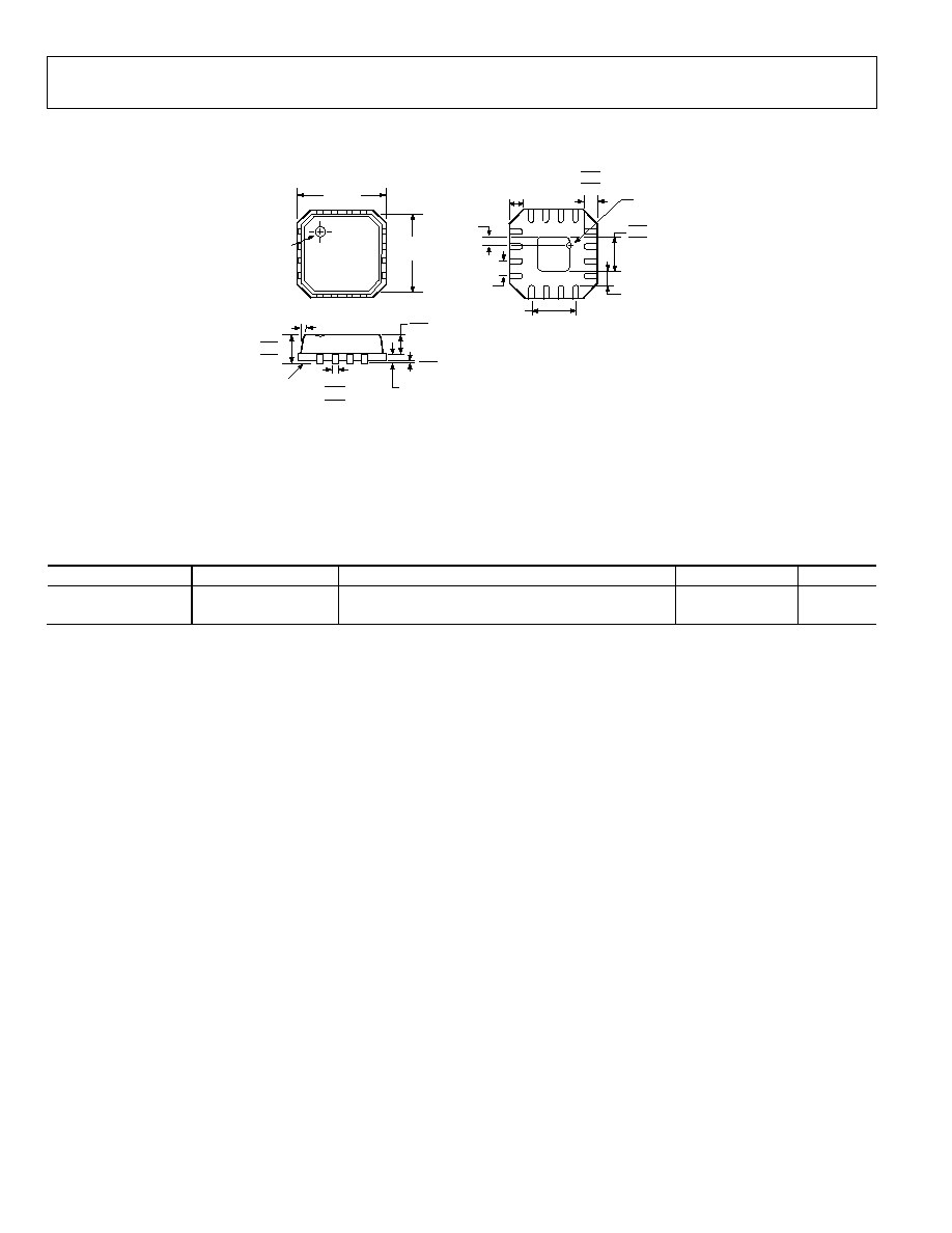
OUTLINE DIMENSIONS
1
0.50
BSC
0.60 MAX
PIN 1
INDICATOR
1.50 REF
0.50
0.40
0.30
0.25 MIN
0.45
2.75
BSC SQ
TOP
VIEW
12° MAX
0.80 MAX
0.65 TYP
SEATING
PLANE
PIN 1
INDICATOR
0.90
0.85
0.80
0.30
0.23
0.18
0.05 MAX
0.02 NOM
0.20 REF
3.00
BSC SQ
*1.65
1.50 SQ
1.35
16
5
13
8
9
12
4
EXPOSED
PAD
(BOTTOM VIEW)
*COMPLIANT TO JEDEC STANDARDS MO-220-VEED-2
EXCEPT FOR EXPOSED PAD DIMENSION.
Figure 32. 16-Lead Lead Frame Chip Scale Package [LFCSP_VQ]
3 mm × 3 mm Body, Very Thin Quad
(CP-16-3)
Dimensions shown in millimeters
ORDERING GUIDE
Model
Temperature Range
Package Description
Package Option
Branding
SSM2304CPZ-REEL
1
-40°C to +85°C
16-Lead Lead Frame Chip Scale Package [LFCSP_VQ]
CP-16-3
A1F
SSM2304CPZ-REEL7
1
-40°C to +85°C
16-Lead Lead Frame Chip Scale Package [LFCSP_VQ]
CP-16-3
A1F
1
Z = Pb-free part.
Rev. PrD | Page 18 of 19

Preliminary Technical Data
SSM2304
NOTES
©2006 Analog Devices, Inc. All rights reserved. Trademarks and
registered trademarks are the property of their respective owners.
PR06162-0-7/06(PrD)
Rev. PrD | Page 19 of 19