 | –≠–ª–µ–∫—Ç—Ä–æ–Ω–Ω—ã–π –∫–æ–º–ø–æ–Ω–µ–Ω—Ç: SSM2412 | –°–∫–∞—á–∞—Ç—å:  PDF PDF  ZIP ZIP |
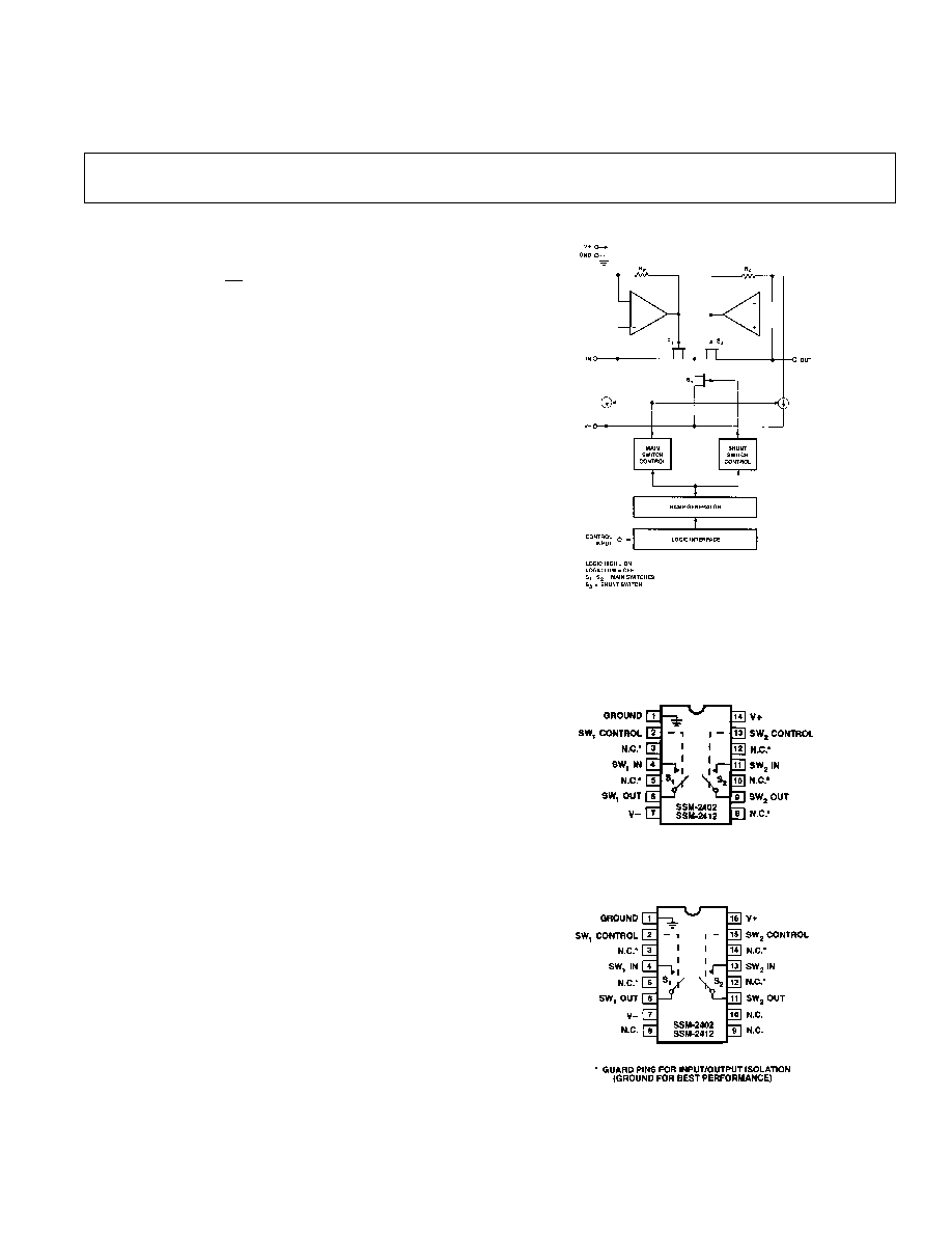
FUNCTIONAL BLOCK DIAGRAM
PIN CONNECTIONS
14-Pin Epoxy DIP
(P-Suffix)
16-Pin SOL
(S-Suffix)
REV. A
Information furnished by Analog Devices is believed to be accurate and
reliable. However, no responsibility is assumed by Analog Devices for its
use, nor for any infringements of patents or other rights of third parties
which may result from its use. No license is granted by implication or
otherwise under any patent or patent rights of Analog Devices.
a
Dual Audio
Analog Switches
SSM2402/SSM2412
One Technology Way, P.O. Box 9106, Norwood, MA 02062-9106, U.S.A.
Tel: 617/329-4700
Fax: 617/326-8703
FEATURES
"Clickless" Bilateral Audio Switching
Guaranteed "Break-Before-Make" Switching
Low Distortion: 0.003% typ
Low Noise: 1 nV/
Hz
Superb OFF-Isolation: 120 dB typ
Low ON-Resistance: 60 typ
Wide Signal Range: V
S
= 18 V; 10 V rms
Wide Power Supply Range: 20 V max
Available in Dice Form
GENERAL DESCRIPTION
The SSM2402/SSM2412 are dual analog switches designed spe-
cifically for high performance audio applications. Distortion and
noise are negligible over the full audio operating range of 20 Hz to
20 kHz at signal levels of up to 10 V rms. The SSM2402/
SSM2412 offer a monolithic integrated alternative to expensive
and noisy relays or complex discrete JFET circuits. Unlike conven-
tional general-purpose CMOS switches, the SSM2402/SSM2412
provide superb fidelity without audio "clicks" during switching.
Conventional TTL or CMOS logic can be used to control the
switch state. No external pull-up resistors are needed. A "T"
configuration provides superb OFF-isolation and true bilateral
operation. The analog inputs and outputs are protected against
overload and overvoltage.
An important feature is the guaranteed "break-before-make"
for all units, even IC-to-IC. In large systems with multiple
switching channels, all separate switching units must open be-
fore any switch goes into the ON-state. With the SSM2402/
SSM2412, you can be certain that multiple circuits will all
break-before-make.
The SSM2402/SSM2412 represent a significant step forward in
audio switching technology. Distortion and switching noise are
significantly reduced in the new SSM2402/SSM2412 bipolar-
JFET switches relative to CMOS switching technology. Based
on a new circuit topology that optimizes audio performance,
the SSM2402/SSM2412 make use of a proprietary bipolar-
JFET process with thin-film resistor network capability. Nitride
capacitors, which are very area efficient, are used for the propri-
etary ramp generator that controls the switch resistance transi-
tion. Very wide bandwidth amplifiers control the gate-to-source
voltage over the full audio operating range for each switch. The
ON-resistance remains constant with changes in signal amplitude
and frequency, thus distortion is very low, less than 0.01% max.
The SSM2402 is the first analog switch truly optimized for
high-performance audio applications. For broadcasting and
other switching applications which require a faster switching
time, we recommend the SSM2412--a dual analog switch with
one-third of the switching time of the SSM2402.
REV. A
≠2≠
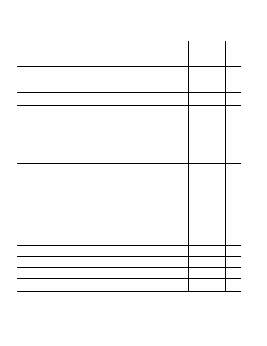
SSM2402/SSM2412≠SPECIFICATIONS
ELECTRICAL CHARACTERISTICS
SSM2402/SSM2412
Parameter
Symbol
Conditions
Min
Typ
Max
Units
POSITIVE SUPPLY CURRENT
+I
SY
V
IL
= 0.8 V, 2.0 V
1
6.0
7.5
mA
NEGATIVE SUPPLY CURRENT
≠I
SY
V
IL
= 0.8 V, 2.0 V
1
4.8
6.0
mA
GROUND CURRENT
I
GND
V
IL
= 0.8 V, 2.0 V
1
0.6
1.5
mA
DIGITAL INPUT HIGH
V
INH
T
A
= Full Temperature Range
20
V
DIGITAL INPUT LOW
V
INL
T
A
= Full Temperature Range
0.8
V
LOGIC INPUT CURRENT
I
LOGIC
V
IN
= 0 V to 15 V
2
1.0
5.0
µ
A
ANALOG VOLTAGE RANGE
3
V
ANALOG
≠14.2
+14.2 V
ANALOG CURRENT RANGE
3
I
ANALOG
≠10
+10
mA
OVERVOLTAGE INPUT CURRENT
V
IN
=
±
V
SUPPLY
±
40
mA
SWITCH ON RESISTANCE
R
ON
≠14.2 V
V
A
+14.2 V
I
A
=
±
10 mA, V
IL
= 2.0 V
T
A
= +25
∞
C
60
85
T
A
= Full Temperature Range
115
Tempco (
R
ON
/
T)
0.2
/
∞
C
R
ON
MATCH
R
ON
MATCH
≠14.2 V
V
A
+14.2 V
1
5
%
I
A
=
±
10 mA, V
IL
= 2.0 V
SWITCH ON LEAKAGE CURRENT
I
S(ON)
V
IL
= 2.0 V
≠14.2 V
V
A
+14.2 V
0.05
1.0
µ
A
V
A
= 0 V
0.05
10.0
nA
SWITCH OFF LEAKAGE CURRENT
I
S(OFF)
V
IL
= 0.8 V
≠14.2 V
V
A
+14.2 V
0.05
1.0
µ
A
V
A
= 0 V
0.05
10.0
nA
TURN-ON TIME
4
t
ON
V
A
= +10 V, R
L
= 2 k
SSM2402
10.0
ms
T
A
= +25
∞
C, See Test Circuit
SSM2412
3.5
TURN-OFF TIME
5
t
OFF
V
A
= +10 V, R
L
= 2 k
SSM2402
4.0
ms
T
A
= +25
∞
C, See Test Circuit
SSM2412
1.5
BREAK-BEFORE-MAKE
t
OFF
≠t
ON
T
A
= +25
∞
C
SSM2402
6.0
ms
TIME DELAY
6
SSM2412
2.0
CHARGE INJECTION
Q
T
A
= +25
∞
C
SSM2402
50
pC
SSM2412
150
ON-STATE INPUT
CS
(ON)
V
A
= 1 V rms
12
pF
CAPACITANCE
f = 5 kHz, T
A
= +25
∞
C
OFF-STATE INPUT
CS
(OFF)
V
A
= 1 V rms
4
pF
CAPACITANCE
f = 5 kHz, T
A
= +25
∞
C
OFF ISOLATION
I
SO(OFF)
V
A
= 10 V rms, 20 Hz to 20 kHz
120
dB
T
A
= +25
∞
C, See Test Circuit
CHANNEL-TO-CHANNEL
C
T
V
A
= 10 V rms, 20 Hz to 20 kHz
96
dB
CROSSTALK
T
A
= +25
∞
C
TOTAL HARMONIC
THD
0 V to 10 V rms, 20 Hz to 20 kHz
0.003 0.01
%
DISTORTION
7
T
A
= +25
∞
C, R
L
= 5 k
SPECTRAL NOISE DENSITY
e
n
20 Hz to 20 kHz, T
A
= +25
∞
C
1
nV/
Hz
WIDEBAND NOISE DENSITY
e
n
p-p
20 Hz to 20 kHz, T
A
= +25
∞
C
0.2
µ
V p-p
NOTES
1
"V
IL
" is the Logic Control Input.
2
Current tested at V
IN
= 0 V. This is the worst case condition.
3
Guaranteed by R
ON
test condition.
4
Turn-ON time is measured from the time the logic input reaches the 50% point to the time the output reaches 50% of the final value.
5
Turn-OFF time is measured from the time the logic input reaches the 50% point to the time the output reaches 50% of the initial value.
6
Switch is guaranteed by design to provide break-before-make operation.
7
THD guaranteed by design and dynamic R
ON
testing.
Specifications subject to change without notice.
(@ V
S
= 18 V, R
L
= OPEN, and ≠40 C
T
A
+85 C unless otherwise noted.
All specifications, tables, graphs, and application data apply to both the SSM2402 and SSM2412, unless otherwise noted.)

SSM2402/SSM2412
REV. A
≠3≠
ABSOLUTE MAXIMUM RATINGS
Operating Temperature Range . . . . . . . . . . . ≠40
∞
C to +85
∞
C
Operating Supply Voltage Range . . . . . . . . . . . . . . . . .
±
20 V
Analog Input Voltage Range
Continuous . . . . . . . . . . . . . . V≠ +3.5 V
V
A
V+ ≠3.5 V
Maximum Current Through Switch . . . . . . . . . . . . . . 20 mA
Logic Input Voltage Range . . . . . . . . . . . . V+ Supply to ≠2 V
V+ Supply to Ground . . . . . . . . . . . . . . . . . . . . . . . . . . +36 V
V≠ Supply to Ground . . . . . . . . . . . . . . . . . . . . . . . . . . . ≠20 V
V
A
to V≠ Supply . . . . . . . . . . . . . . . . . . . . . . . . . . . . . . +36 V
Package Type
JA
*
JC
Units
14-Pin Plastic DIP (P)
76
33
∞
C/W
16-Pin SOL (S)
92
27
∞
C/W
*
JA
is specified for worst case mounting conditions, i.e.,
JA
is specified for device
in socket for P-DIP package;
JA
is specified for device soldered to printed circuit
board for SOL package.
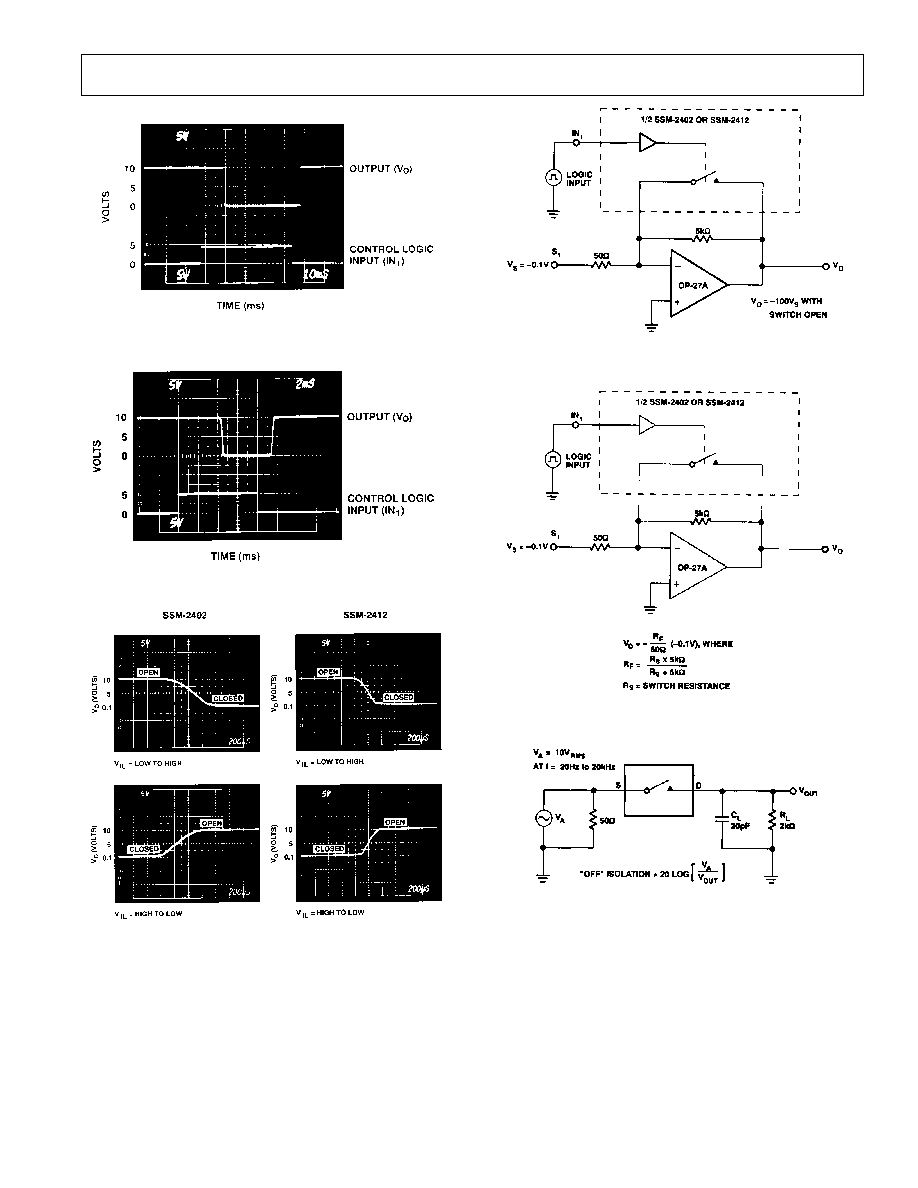
Timing Diagram
ORDERING GUIDE
Temperature
Package
Model
Range
Description
SSM2402P
≠40
∞
C to +85
∞
C
14-Pin Plastic DIP
SSM2402S
≠40
∞
C to +85
∞
C
16-Pin SOL
SSM2412P
≠40
∞
C to +85
∞
C
14-Pin Plastic DIP
SSM2412S
≠40
∞
C to +85
∞
C
16-Pin SOL
DICE CHARACTERISTICS
Die Size 0.105
◊
0.097 Inch, 10,185 sq. mils
(2.667
◊
2.464 mm, 6.57 sq. mm)
WAFER TEST LIMITS
Parameter
Symbol
Conditions
1
Limit
Units
POSITIVE SUPPLY CURRENT
+I
SY
V
IL
= 0.8 V
7.5
mA max
NEGATIVE SUPPLY CURRENT
≠I
SY
V
IL
= 0.8 V
6.0
mA max
GROUND CURRENT
I
GND
V
IL
= 0.8 V
1.5
mA max
LOGIC INPUT CURRENT
I
LOGIC
V
IN
= 0 V
2
5.0
µ
A max
SWITCH ON RESISTANCE
R
ON
≠14.2 V
V
A
+14.2 V
85
max
I
A
=
±
10 mA, V
IL
= 2.0 V
R
ON
MATCH BETWEEN SWITCHES
R
ON
MATCH
≠14.2 V
V
A
+14.2 V
5
% max
I
A
=
±
10 mA, V
IL
= 2.0 V
SWITCH ON LEAKAGE CURRENT
I
S(ON)
≠14.2 V
V
A
+14.2 V, V
IL
= 2.0 V
1.0
µ
A max
SWITCH OFF LEAKAGE CURRENT
I
S(OFF)
≠14.2 V
V
A
+14.2 V, V
IL
= 0.8 V
1.0
µ
A max
NOTES
1
V
IL
= Logic Control Input; V
A
= Applied Analog Input Voltage; I
A
= Applied Analog Input Current.
2
Worst Case Condition.
Electrical tests are performed at wafer probe to the limits shown. Due to variations in assembly methods and normal yield loss, yield after packaging is not
guaranteed for standard product dice. Consult factory to negotiate specifications based on dice lot qualifications through sample lot assembly and testing.

"ON" Resistance vs. Analog Voltage
Channel Separation vs. Frequency
Leakage Current vs. Analog Voltage
Total Harmonic Distortion vs.
Frequency
SSM2402 Switching Time
vs. Temperature
Supply Current vs. Temperature
"OFF" Isolation vs. Frequency
SSM2412 Switching Time
vs. Temperature
Overvoltage Characteristics
SSM2402/SSM2412≠Typical Performance Characteristics
REV. A
≠4≠
SSM2402/SSM2412
REV. A
≠5≠
SSM2402 T
ON
/T
OFF
Switching Response
SSM 2412 T
ON
/T
OFF
Switching Response
Switching ON/OFF Transition
T
ON
/T
OFF
Switching Response Test Circuit
Switch ON/OFF Transition Test Circuit
"OFF" Isolation Test Circuit