 | –≠–ª–µ–∫—Ç—Ä–æ–Ω–Ω—ã–π –∫–æ–º–ø–æ–Ω–µ–Ω—Ç: SSM2475S | –°–∫–∞—á–∞—Ç—å:  PDF PDF  ZIP ZIP |

8-Lead Narrow Body SOIC 14-Lead Narrow Body SOIC
(SO-8)
(R-14)
8-Lead microSOIC 14-Lead TSSOP
(RM-8) (RU-14)
8-Lead Plastic DIP
(N-8)
REV. A
Information furnished by Analog Devices is believed to be accurate and
reliable. However, no responsibility is assumed by Analog Devices for its
use, nor for any infringements of patents or other rights of third parties
which may result from its use. No license is granted by implication or
otherwise under any patent or patent rights of Analog Devices.
a
Rail-to-Rail Output
Audio Amplifiers
SSM2275/SSM2475*
One Technology Way, P.O. Box 9106, Norwood. MA 02062-9106, U.S.A.
Tel: 781/329-4700 World Wide Web Site: http://www.analog.com
Fax: 781/326-8703 © Analog Devices, Inc., 1999
GENERAL DESCRIPTION
The SSM2275 and SSM2475 use the Butler Amplifier front
end, which combines both bipolar and FET transistors to offer
the accuracy and low noise performance of bipolar transistors
and the slew rates and sound quality of FETs. This product
family includes dual and quad rail-to-rail output audio amplifi-
ers that achieve lower production costs than the industry stan-
dard OP275 (the first Butler Amplifier offered by Analog
Devices). This lower cost amplifier also offers operation from a
single 5 V supply, in addition to conventional
±
15 V supplies.
The ac performance meets the needs of the most demanding au-
dio applications, with 8 MHz bandwidth, 12 V/
µ
s slew rate and
extremely low distortion.
The SSM2275 and SSM2475 are ideal for application in high
performance audio amplifiers, recording equipment, synthesiz-
ers, MIDI instruments and computer sound cards. Where cas-
caded stages demand low noise and predictable performance,
SSM2275 and SSM2475 are a cost effective solution. Both are
stable even when driving capacitive loads.
The ability to swing rail-to-rail at the outputs (see Applications sec-
tion) and operate from low supply voltages enables designers to at-
tain high quality audio performance, even in single supply systems.
The SSM2275 and SSM2475 are specified over the extended
industrial (≠40
∞
C to +85
∞
C) temperature range. The SSM2275 is
available in 8-lead plastic DIPs, SOICs, and microSOIC surface-
mount packages. The SSM2475 is available in narrow body
SOICs and thin shrink small outline (TSSOP) surface-mount
packages.
*Protected by U.S. Patent No. 5,101,126.
FEATURES
Single or Dual-Supply Operation
Excellent Sonic Characteristics
Low Noise: 7 nV/
Hz
Low THD: 0.0006%
Rail-to-Rail Output
High Output Current: 50 mA
Low Supply Current: 1.7 mA/Amplifier
Wide Bandwidth: 8 MHz
High Slew Rate: 12 V/ s
No Phase Reversal
Unity Gain Stable
Stable Parameters Over Temperature
APPLICATIONS
Multimedia Audio
Professional Audio Systems
High Performance Consumer Audio
Microphone Preamplifier
MIDI Instruments
PIN CONFIGURATIONS
1
2
3
4
8
7
6
5
(Not to Scale)
OUT A
≠IN A
+IN A
V≠
OUT B
≠IN B
+IN B
V+
SSM2275
OUT A
≠IN A
+IN A
V+
≠IN D
+IN D
V≠
OUT D
1
2
3
4
5
6
7
14
13
12
11
10
9
8
+IN B
≠IN B
OUT B
≠IN C
OUT C
+IN C
SSM2475
(Not to Scale)
≠IN A
+IN A
V≠
OUT B
≠IN B
+IN B
V+
1
4
5
8
SSM2275
OUT A
OUT A
≠IN A
+IN A
V+
≠IN D
+IN D
V≠
OUT D
1
14
+IN B
≠IN B
OUT B
≠IN C
OUT C
+IN C
7
8
SSM2475
1
2
3
4
8
7
6
5
(Not to
Scale)
SSM2275
OUT A
≠IN A
+IN A
V≠
+IN B
≠IN B
OUT B
V+
REV. A
≠2≠
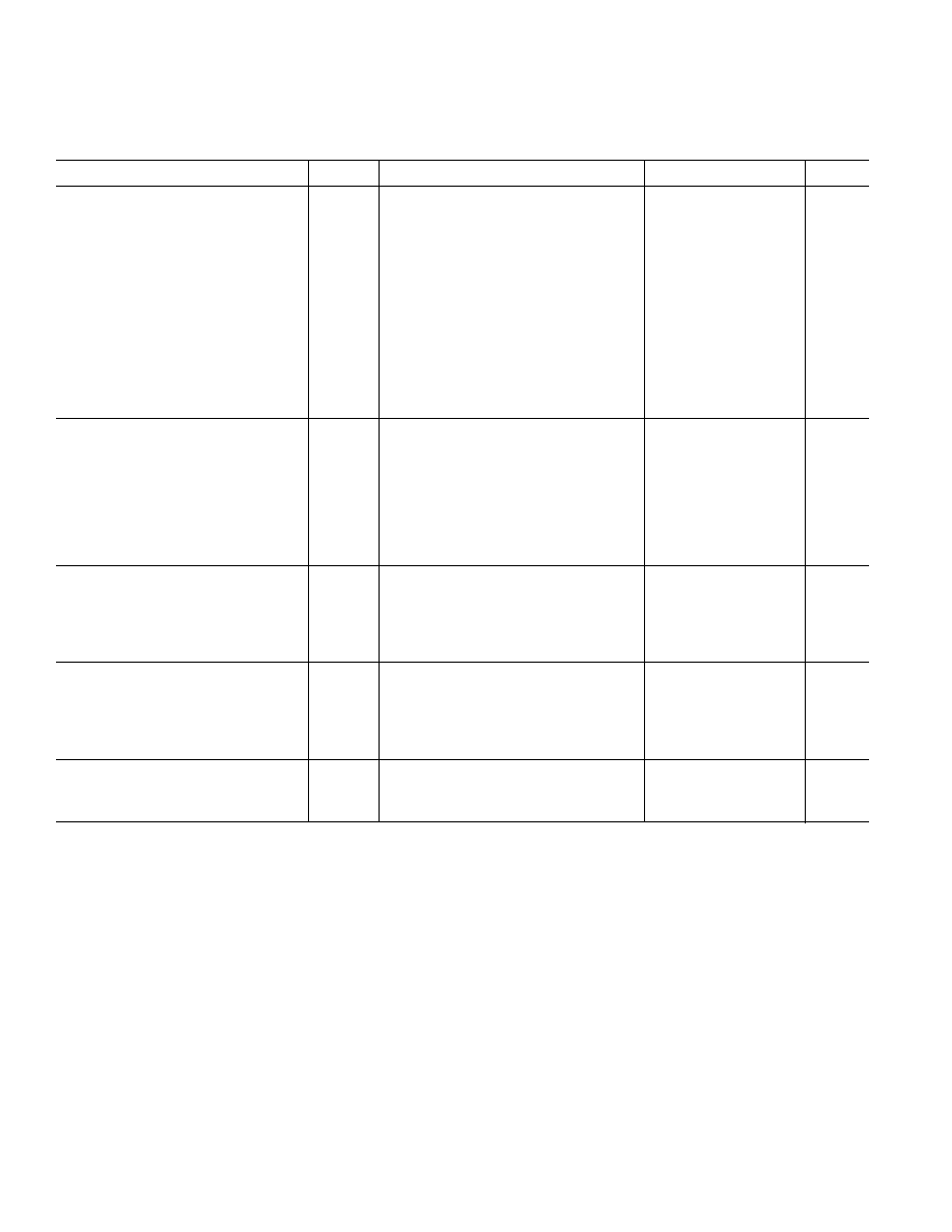
SSM2275/SSM2475≠SPECIFICATIONS
ELECTRICAL CHARACTERISTICS
Parameter
Symbol
Conditions
Min
Typ
Max
Units
INPUT CHARACTERISTICS
Offset Voltage
V
OS
1
4
mV
≠40
∞
C
T
A
+85
∞
C
1
6
mV
Input Bias Current
I
B
250
400
nA
≠40
∞
C
T
A
+85
∞
C
300
500
nA
Input Offset Current
I
OS
5
75
nA
≠40
∞
C
T
A
+85
∞
C
15
125
nA
Input Voltage Range
V
IN
V
S
=
±
15 V
≠14
+14
V
Common-Mode Rejection Ratio
CMRR
≠12.5 V
V
CM
+12.5 V
80
100
dB
≠40
∞
C
T
A
+85
∞
C,
≠12.5 V
V
CM
+12.5 V
80
100
V/mV
A
VO
R
L
= 2 k
, ≠12 V
V
O
+12 V
100
240
V/mV
≠40
∞
C
T
A
+85
∞
C
80
120
V/mV
OUTPUT CHARACTERISTICS
Output Voltage, High
V
OH
I
L
20 mA
14
14.5
V
≠40
∞
C
T
A
+85
∞
C
14.5
14.7
V
Output Voltage, Low
V
OL
I
L
= 20 mA
≠14
≠13.5
V
I
L
= 10 mA
≠14.6 ≠14.4
V
I
L
= 10 mA, ≠40
∞
C
T
A
+85
∞
C
≠14.3 ≠13.9
V
Output Short Circuit Current Limit
I
SC
±
25
±
50
±
75
mA
≠40
∞
C
T
A
+85
∞
C
±
17
±
40
±
80
mA
POWER SUPPLY
Power Supply Rejection Ratio
PSRR
±
2.5 V
V
S
±
18 V
85
110
dB
≠40
∞
C
T
A
+85
∞
C
80
105
dB
Supply Current/Amplifier
I
SY
V
O
= 0 V
1.7
2.9
mA
≠40
∞
C
T
A
+85
∞
C
1.75
3.0
mA
DYNAMIC PERFORMANCE
Total Harmonic Distortion
THD
R
L
= 10 k
, f = 1 kHz, V
O
= 1 V rms
0.0006
%
Slew Rate
SR
R
L
= 2 k
50 pF
9
12
V/
µ
s
Gain Bandwidth Product
GBW
8
MHz
Channel Separation
CS
R
L
= 2 k
, f =1 kHz
128
dB
NOISE PERFORMANCE
Voltage Noise Spectral Density
e
n
f > 1 kHz
8
nV/
Hz
Current Noise Spectral Density
i
n
f > 1 kHz
< 1
pA/
Hz
Specifications subject to change without notice.
(V
S
= 15 V, T
A
= 25 C, V
CM
= 0 V unless otherwise noted)
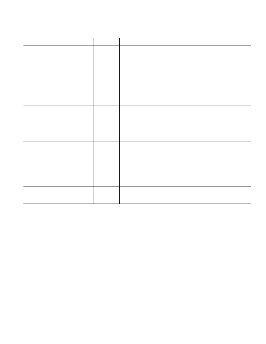
ELECTRICAL CHARACTERISTICS
Parameter
Symbol
Conditions
Min
Typ
Max
Units
INPUT CHARACTERISTICS
Offset Voltage
V
OS
1
4
mV
≠40
∞
C
T
A
+85
∞
C
1
6
mV
Input Bias Current
I
B
250
400
nA
≠40
∞
C
T
A
+85
∞
C
300
500
nA
Input Offset Current
I
OS
5
75
nA
≠40
∞
C
T
A
+85
∞
C
15
125
nA
Input Voltage Range
V
IN
0.3
4.7
V
Common-Mode Rejection Ratio
CMRR
+0.8 V
V
CM
+2 V
85
dB
≠40
∞
C
T
A
+85
∞
C
80
dB
A
VO
R
L
= 2 k
, ≠0.5 V
V
O
+4.5 V
25
60
V/mV
≠40
∞
C
T
A
+85
∞
C
20
50
V/mV
OUTPUT CHARACTERISTICS
Output Voltage, High
V
OH
I
L
≠15 mA
4.2
4.5
V
I
L
≠10 mA, ≠40
∞
C
T
A
+85
∞
C
4.5
4.8
V
Output Voltage, Low
V
OL
I
L
≠15 mA
0.6
1.0
V
I
L
≠10 mA
0.3
0.5
V
I
L
≠10 mA, ≠40
∞
C
T
A
+85
∞
C
0.7
1.1
V
Output Short Circuit Current Limit
I
SC
≠40
∞
C
T
A
+85
∞
C
40
mA
POWER SUPPLY
Supply Current/Amplifier
I
SY
V
O
= 0 V
1.7
2.9
mA
≠40
∞
C
T
A
+85
∞
C
1.75
3.0
mA
DYNAMIC PERFORMANCE
Total Harmonic Distortion
THD
R
L
= 10 k
, f = 1 kHz, V
O
= 1 V rms
0.0006
%
Slew Rate
SR
R
L
= 2 k
50 pF
12
V/
µ
s
Gain Bandwidth Product
GBW
R
L
= 2 k
10 pF
6
MHz
Channel Separation
CS
R
L
= 2 k
, f =1 kHz
128
dB
NOISE PERFORMANCE
Voltage Noise Spectral Density
e
n
f > 1 kHz
8
nV/
Hz
Current Noise Spectral Density
i
n
f > 1 kHz
< 1
pA/
Hz
Specifications subject to change without notice.
REV. A
≠3≠
SSM2275/SSM2475
(V
S
= 5 V, T
A
= 25 C, V
CM
= 2.5 V unless otherwise noted)

SSM2275/SSM2475
REV. A
≠4≠
ABSOLUTE MAXIMUM RATINGS
1
Supply Voltage (V
S
) . . . . . . . . . . . . . . . . . . . . . . . . . . . .
±
18 V
Input Voltage (V
IN
) . . . . . . . . . . . . . . . . . . . . . . . . . . . .
±
15 V
Differential Input Voltage
2
. . . . . . . . . . . . . . . . . . . . . . .
±
15 V
Storage Temperature Range . . . . . . . . . . . .
65
∞
C to 150
∞
C
Operating Temperature Range . . . . . . . . . . .
40
∞
C to 85
∞
C
Junction Temperature Range . . . . . . . . . . . .
65
∞
C to 150
∞
C
Lead Temperature Range (Soldering, 60 sec) . . . . . . .
300
∞
C
ESD Susceptibility . . . . . . . . . . . . . . . . . . . . . . . . . . . . 2,000 V
NOTES
1
Stresses above those listed under Absolute Maximum Ratings may cause perma -
nent damage to the device. This is a stress rating only; the functional operation of
the device at these or any other conditions above those indicated in the opera tional
sections of this specification is not implied. Exposure to absolute maximum rating
conditions for extended periods may affect device reliability.
2
For supplies less than
±
15 V, the input voltage and differential input voltage
must be less than
±
15 V.
Package Type
JA
*
JC
Units
8-Lead Plastic DIP
103
43
∞
C/W
8-Lead SOIC
158
43
∞
C/W
8-Lead microSOIC
206
43
∞
C/W
14-Lead SOIC
120
36
∞
C/W
14-Lead TSSOP
180
35
∞
C/W
*
JA
is specified for the worst case conditions, i.e., for device in socket for DIP
packages and soldered onto a circuit board for surface mount packages.
ORDERING GUIDE
Temperature
Package
Package
Model
Range
Description
Options
SSM2275P
≠40
∞
C to +85
∞
C
8-Lead PDIP
N-8
SSM2275S
≠40
∞
C to +85
∞
C
8-Lead SOIC
SO-8
SSM2275RM
≠40
∞
C to +85
∞
C
8-Lead microSOIC
RM-8
SSM2475S
≠40
∞
C to +85
∞
C
14-Lead SOIC
R-14
SSM2475RU
≠40
∞
C to +85
∞
C
14-Lead TSSOP
RU-14
CAUTION
ESD (electrostatic discharge) sensitive device. Electrostatic charges as high as 4000 V readily
accumulate on the human body and test equipment and can discharge without detection.
Although the SSM2275/SSM2475 features proprietary ESD protection circuitry, permanent
damage may occur on devices subjected to high energy electrostatic discharges. Therefore, proper
ESD precautions are recommended to avoid performance degradation or loss of functionality.
WARNING!
ESD SENSITIVE DEVICE
FREQUENCY ≠ Hz
100
80
≠40
10
1M
100
GAIN ≠ dB
1k
10k
100k
60
40
20
0
≠20
10M 40M
PHASE ≠ Degrees
225
180
≠90
135
90
45
0
≠45
V
S
= 2.5V
R
L
= 2k
C
L
= 10pF
Figure 1. Phase/Gain vs. Frequency
FREQUENCY ≠ Hz
100
80
≠40
10
1M
100
GAIN ≠ dB
1k
10k
100k
60
40
20
0
≠20
10M 40M
PHASE ≠ Degrees
225
180
≠90
135
90
45
0
≠45
V
S
= 2.5V
R
L
= 600
C
L
= 10pF
Figure 2. Phase/Gain vs. Frequency

FREQUENCY ≠ Hz
100
80
≠40
10
1M
100
GAIN ≠ dB
1k
10k
100k
60
40
20
0
≠20
10M 40M
PHASE ≠ De
g
rees
225
180
≠90
135
90
45
0
≠45
V
S
= 15V
R
L
= 2k
C
L
= 10pF
Figure 3. Phase/Gain vs. Frequency
FREQUENCY ≠ Hz
100
80
≠40
10
1M
100
GAIN ≠ dB
1k
10k
100k
60
40
20
0
≠20
10M 40M
PHASE ≠ De
g
rees
225
180
≠90
135
90
45
0
≠45
V
S
= 15V
R
L
= 600
C
L
= 10pF
Figure 4. Phase/Gain vs. Frequency
FREQUENCY ≠ Hz
2.0
1.8
0.2
10
10k
100
CURRENT NOISE DENSITY ≠ pA/
Hz
1k
1.6
1.4
0.6
1.2
1.0
0.8
0.4
V
S
= 15V
T
A
= 25 C
Figure 5. SSM2275 Current Noise Density vs. Frequency
FREQUENCY ≠ Hz
60
50
0
10
100k
100
VOLTAGE NOISE DENSITY ≠ nV/
Hz
1k
10k
40
30
10
20
V
S
= 15V
T
A
= 25 C
Figure 6. SSM2275 Voltage Noise Density (Typical)
FREQUENCY ≠ Hz
140
120
0
100
30M
1k
COMMON MODE REJECTION ≠ dB
10k
1M
10M
100
80
60
40
20
V
S
= 15V
T
A
= 25 C
Figure 7. Common-Mode Rejection vs. Frequency
FREQUENCY ≠ Hz
140
120
0
100
10M
1k
POWER SUPPLY REJECTION ≠ dB
10k
1M
100
80
60
40
20
V
S
= 15V
T
A
= 25 C
Figure 8. Power Supply Rejection vs. Frequency
Typical Characteristics≠SSM2275/SSM2475
REV. A
≠5≠