Advanced Monolithic Systems, Inc. 6680B Sierra Lane, Dublin, CA 94568 Phone (925) 556-9090 Fax (925) 556-9140
Advanced
AMS1508
Monolithic
8A LOW DROPOUT VOLTAGE REGULATOR
Systems
FEATURES
APPLICATIONS
∑
∑
Adjustable or Fixed Output
∑
∑
High Current Regulators
1.5V, 2.5V, 2.85V, 3.0V, 3.3V, 3.5V and 5.0V
∑
∑
Post Regulators for Switching Supplies
∑
∑
Output Current of 8A
∑
∑
Microprocessor Supply
∑
∑
Low Dropout, 500mV at 8A Output Current
∑
∑
Adjustable Power Supply
∑
∑
Fast Transient Response
∑
∑
Notebook/Personal Computer Supplies
∑
∑
Remote Sense
GENERAL DESCRIPTION
The
The AMS1508 series of adjustable and fixed low dropout voltage regulators are designed to provide 8A output current to
power the new generation of microprocessors. The dropout voltage of the device is 100mV at light loads and rising to 500mV
at maximum output current. A second low current input voltage 1V or greater then the output voltage is required to achieve
this dropout. The AMS1508 can also be used as a single supply device.
New features have been added to the AMS1508: a remote Sense pin is brought out virtually eliminating output voltage
variations due to load changes. The typical load regulation, measured at the Sense pin, for a load current step of 100mA to 8A
is less than 1mV.
The AMS1508 series has fast transient response. The Adjust pin is brought out on fixed devices. To further improve the
transient response the addition of a small capacitor on the Adjust pin is recommended.
The AMS1508 series are ideal for generating processor supplies of 2V to 3V on motherboards where both 5V and 3.3V
supplies are available.
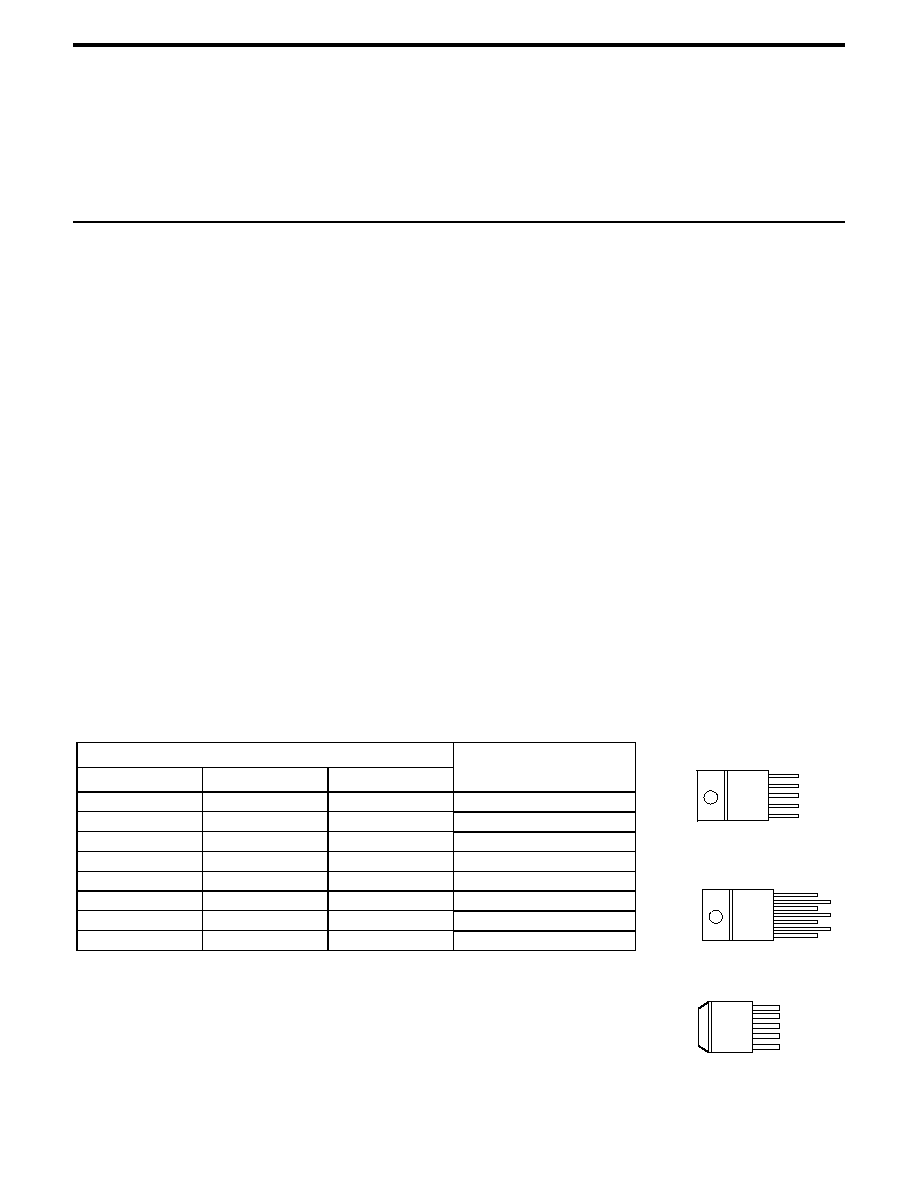
The AMS1508 devices are offered in 5 lead TO-220 and TO-263 (plastic DD) packages and in the 7 lead TO-220 package.
ORDERING INFORMATION:
PIN CONNECTIONS
PACKAGE TYPE
OPERATING JUNCTION
5 LEAD TO-263
5 LEAD TO-220
7 LEAD TO-220 TEMPERATURE RANGE
AMS1508CM
AMS1508CT
AMS1508CT-1.5
0 to 125
∞
C
AMS1508CM-1.5 AMS1508CT-1.5
AMS1508CT-2.5
0 to 125
∞
C
AMS1508CM-2.5 AMS1508CT-2.5
AMS1508CT-2.85
0 to 125
∞
C
AMS1508CM-2.85 AMS1508CT-2.85 AMS1508CT-3.0
0 to 125
∞
C
AMS1508CM-3.0 AMS1508CT-3.0
AMS1508CT-3.3
0 to 125
∞
C
AMS1508CM-3.3 AMS1508CT-3.3
AMS1508CT-3.5
0 to 125
∞
C
AMS1508CM-3.5 AMS1508CT-3.5
AMS1508CT-5.0
0 to 125
∞
C
AMS1508CM-5.0 AMS1508CT-5.0
0 to 125
∞
C
5
4
3
2
1
V
POWER
V
CONTROL
OUTPUT
ADJUST/GND
SENSE
FRONT VIEW
5 LEAD TO-220
7
6
5
4
3
2
1
NC
Vpower
ADJUST
OUTPUT
Vcontrol
GND
SENSE
7 LEAD TO-220
FRONT VIEW
5
4
3
2
1
Vpower
Vcontrol
OUTPUT
ADJUST/GND
SENSE
FRONT VIEW
5 LEAD TO-263

Advanced Monolithic Systems, Inc. 6680B Sierra Lane, Dublin, CA 94568 Phone (925) 556-9090 Fax (925) 556-9140
AMS1508
ABSOLUTE MAXIMUM RATINGS
(Note 1)
V
POWER
Input Voltage
7V
Soldering information
V
CONTROL
Input Voltage
13V
Lead Temperature (10 sec)
300
∞
C
Operating Junction Temperature Range
Thermal Resistance
Control Section
0
∞
C to 125
∞
C
TO-220 package
JA
= 50
∞
C/W
Power Transistor
0
∞
C to 150
∞
C
TO-263 package
JA
= 30
∞
C/W*
Storage temperature
- 65
∞
C to +150
∞
C
* With package soldering to 0.5in
2
copper area over backside ground
plane or internal power plane
JA
can vary from 20
∞
C/W to
>
40
∞
C/W
depending on mounting technique.
ELECTRICAL CHARACTERISTICS
Electrical Characteristics at I
LOAD
= 0 mA, and T
J
= +25∞C unless otherwise specified.
Parameter
Device
Conditions
Min Typ Max
Units
Reference Voltage
AMS1508
V
CONTROL
= 2.75V, V
POWER
=2V, I
LOAD
= 10mA
V
CONTROL
= 2.7V to 12V, V
POWER
=3.3V to 5.5V,
I
LOAD
= 10mA to 8A
1.243
1.237
1.250
1.250
1.258
1.263
V
V
Output Voltage
AMS1508-1.5
V
CONTROL
= 4V, V
POWER
=2.V, I
LOAD
= 0mA
V
CONTROL
= 3V, V
POWER
=2.3V, I
LOAD
= 0mA to 8A
1.491
1.485
1.500
1.500
1.509
1.515
V
V
AMS1508-2.5
V
CONTROL
= 5V, V
POWER
=3.3V, I
LOAD
= 0mA
V
CONTROL
= 4V, V
POWER
=3.3V, I
LOAD
= 0mA to 8A
2.485
2.475
2.500
2.500
2.515
2.525
V
V
AMS1508-2.85
V
CONTROL
= 5.35V, V
POWER
=3.35V, I
LOAD
= 0mA
V
CONTROL
= 4.4V, V
POWER
=3.7V, I
LOAD
= 0mA to 8A
2.821
2.833
2.850
2.850
2.879
2.867
V
V
AMS1508-3.0
V
CONTROL
= 5.5V, V
POWER
=3.5V, I
LOAD
= 0mA
V
CONTROL
= 4.5V, V
POWER
=3.8V, I
LOAD
= 0mA to 8A
2.982
2.970
3.000
3.000
3.018
3.030
V
V
AMS1508-3.3
V
CONTROL
= 5.8V, V
POWER
=3.8V, I
LOAD
= 0mA
V
CONTROL
= 4.8V, V
POWER
=4.1V, I
LOAD
= 0mA to 8A
3.280
3.235
3.300
3.300
3.320
3.333
V
V
AMS1508-3.5
V
CONTROL
= 6V, V
POWER
=4V, I
LOAD
= 0mA
V
CONTROL
= 5V, V
POWER
=4.3V, I
LOAD
= 0mA to 8A
3.479
3.430
3.500
3.500
3.521
3.535
V
V
AMS1508-5.0
V
CONTROL
= 7.5V, V
POWER
=5.5V, I
LOAD
= 0mA
V
CONTROL
= 6.5V, V
POWER
=5.8V, I
LOAD
= 0mA to 8A
4.930
4.950
5.000
5.000
5.030
5.050
V
V
Line Regulation
AMS1508/-1.5/-2.5/-2.85/
-3.0/-3.3/-3.5/-5.0
I
LOAD
= 10 mA , 1.5V
(V
CONTROL
- V
OUT
)
12V
0.8V
(V
POWER
- V
OUT
)
5.5V
1
3
mV
Load Regulation
AMS1508/-1.5/-2.5/-2.85/
-3.0/-3.3/-3.5/-5.0
V
CONTROL
= V
OUT
+ 2.5V, V
POWER
=V
OUT
+ 0.8V,
I
LOAD
= 10mA to 8A
1
5
mV
Minimum Load
Current
AMS1508
V
CONTROL
= 5V, V
POWER
=3.3V, V
ADJ
= 0V (Note 3)
5
10
mA
Control Pin Current
(Note 4)
AMS1508/-1.5/-2.5/-2.85/
-3.0/-3.3/-3.5/-5.0
V
CONTROL
= V
OUT
+ 2.5V, V
POWER
=V
OUT
+ 0.8V,
I
LOAD
= 10mA to 8A
80
135
mA
Ground Pin Current
(Note 4)
AMS1508-1.5/-2.5/-2.85/
-3.0/-3.3/-3.5/-5.0
V
CONTROL
= V
OUT
+ 2.5V, V
POWER
=V
OUT
+ 0.8V,
I
LOAD
= 10mA to 8A
6
10
mA
Adjust Pin Current
AMS1508
V
CONTROL
= 2.75V, V
POWER
= 2.05V, I
LOAD
= 10mA
50
120
µ
A
Current Limit
AMS1508/-1.5/-2.5/-2.85/
-3.0/-3.3/-3.5/-5.0
(V
IN
- V
OUT
) = 5V
7.1
8.0
A
Ripple Rejection
AMS1508/-1.5/-2.5/-2.85/
-3.0/-3.3/-3.5/-5.0
V
CONTROL
= V
POWER
= V
OUT
+ 2.5V, V
RIPPLE
= 1V
P-P
I
LOAD
= 4A
60
80
dB
Thermal Regulation
AMS1508
T
A
= 25∞C, 30ms pulse
0.002
0.020
%W
Thermal Resistance
Junction-to-Case
T Package: Control Circuitry/ Power Transistor
M Package: Control Circuitry/ Power Transistor
0.65/2.70
0.65/2.70
∞C/W
∞C/W

Advanced Monolithic Systems, Inc. 6680B Sierra Lane, Dublin, CA 94568 Phone (925) 556-9090 Fax (925) 556-9140
AMS1508
ELECTRICAL CHARACTERISTICS
Electrical Characteristics at I
OUT
= 0 mA, and T
J
= +25∞C unless otherwise specified.
Parameter
Device
Conditions
Min Typ Max
Units
Dropout Voltage
Note 2
Control Dropout
(V
CONTROL
- V
OUT
)
AMS1508/-1.5/-2.5/-2.85/
-3.0/-3.3/-3.5/-5.0
V
POWER
=V
OUT
+ 0.8V, I
LOAD
= 10mA
V
POWER
=V
OUT
+ 0.8V, I
LOAD
= 8A
1.00
1.15
1.15
1.30
V
V
Power Dropout
(V
POWER
- V
OUT
)
AMS1508/-1.5/-2.5/-2.85/
-3.0/-3.3/-3.5/-5.0
V
CONTROL
=V
OUT
+ 2.5V, I
LOAD
= 10mA
V
CONTROL
=V
OUT
+ 2.5V, I
LOAD
= 8A
.10
.45
0.17
0.50
V
V
Parameters identified with boldface type apply over the full operating temperature range.
Note 1:
Absolute Maximum Ratings indicate limits beyond which damage to the device may occur. For guaranteed specifications and test conditions, see the
Electrical Characteristics
.
The guaranteed specifications apply only for the test conditions listed.
Note 2:
Unless otherwise specified V
OUT
= V
SENSE
. For the adjustable device V
ADJ
= 0V.
Note 3:
The dropout voltage for the AMS1508 is caused by either minimum control voltage or minimum power voltage. The specifications represent the minimum
input/output voltage required to maintain 1% regulation.
Note 4:
For the adjustable device the minimum load current is the minimum current required to maintain regulation. Normally the current in the resistor divider
used to set the output voltage is selected to meet the minimum load current requirement.
Note 5:
The control pin current is the drive current required for the output transistor. This current will track output current with a ratio of about 1:100. The
minimum value is equal to the quiescent current of the device.
PIN FUNCTIONS
Sense (Pin 1): This pin is the positive side of the
reference voltage for the device. With this pin it is
possible to Kelvin sense the output voltage at the load.
Adjust (Pin 2/5): This pin is the negative side of the
reference voltage for the device. Adding a small bypass
capacitor from the Adjust pin to ground improves the
transient response. For fixed voltage devices the Adjust
pin is also brought out to allow the user to add a bypass
capacitor.
GND (Pin 2, 7-Lead only): For fixed voltage devices this
is the bottom of the resistor divider that sets the output
voltage.
V
POWER
(Pin 5/6): This pin is the collector to the power
device of the AMS1508. The output load current is
supplied through this pin. The voltage at this pin must
be between 0.1V and 0.8V greater than the output
voltage for the device to regulate.
V
CONTROL
(Pin 4/3): This pin is the supply pin for the
control circuitry of the device. The current flow into
this pin will be about 1% of the output current. The
voltage at this pin must be 1.3V or greater than the
output voltage for the device to regulate.
Output (Pin 3/4): This is the power output of the
device.
Advanced Monolithic Systems, Inc. 6680B Sierra Lane, Dublin, CA 94568 Phone (925) 556-9090 Fax (925) 556-9140
AMS1508
APPLICATION HINTS
The AMS1508 series of adjustable and fixed regulators are
designed to power the new generation of microprocessors. The
AMS1508 is designed to make use of multiple power supplies,
existing in most systems, to reduce the dropout voltage. One of
the advantages of the two supply approach is maximizing the
efficiency.
The second supply is at least 1V greater than output voltage and
is providing the power for the control circuitry and supplies the
drive current to the NPN output transistor. This allows the NPN
to be driven into saturation; thereby reducing the dropout voltage
by a VBE compared to conventional designs. For the control
voltage the current requirement is small equal to about 1% of the
output current or approximately 70mA for a8A load. Most of this
current is drive current for the NPN output transistor. This drive
current becomes part of the output current. The maximum voltage
on the Control pin is 13V. The maximum voltage at the Power
pin is 7V. Ground pin current for fixed voltage devices is typical
6mA and is constant as a function of load. Adjust pin current for
adjustable devices is 60
µ
A at 25
∞
C and varies proportional to
absolute temperature.
The improved frequency compensation of AMS1508 permits the
use of capacitors with very low ESR. This is critical in addressing
the needs of modern, low voltage high sped microprocessors. The
new generation of microprocessors cycle load current from several
hundred mA to several A in tens of nanoseconds. Output voltage
tolerances are tighter and include transient response as part of the
specification. Designed to meet the fast current load step
requirements of these microprocessors, the AMS1508 also saves
total cost by needing less output capacitance to maintain
regulation.
Careful design of the AMS1508 has eliminated any supply
sequencing issues associated with a dual supply system. The
output voltage will not turn on until both supplies are operating.
If the control voltage comes up first, the output current will be
limited to a few milliamperes until the power input voltage comes
up. If power input comes up first the output will not turn on at all
until the control voltage comes up. The output can never come up
unregulated. By tying the control and power inputs together the
AMS1508 can also be operated as a single supply device. In
single supply operation the dropout will be determined by the
minimum control voltage.
The new features of the AMS1508 require additional pins over
the traditional 3-terminal regulator. Both the fixed and adjustable
versions have remote sense pins, permitting very accurate
regulation of output voltage at the load, rather than at the
regulator. As a result, over an output current range of 100mA to
8A with a 2.5V output, the typical load regulation is less than
1mV. For the fixed voltages the adjust pin is brought out allowing
the user to improve transient response by bypassing the internal
resistor divider. Optimum transient response is provided using a
capacitor in the range of 0.1
µ
F to 1
µ
F for bypassing the Adjust
pin. The value chosen will depend on the amount of output
capacitance in the system.
In addition to the enhancements mentioned, the reference
accuracy has been improved by a factor of two with a guaranteed
initial tolerance of
±
0.6% at 25
∞
C. This device can hold 1%
accuracy over the full temperature range and load current range,
guaranteed, when combined with ratiometrically accurate internal
divider resistors and operating with an input/output differential of
well under 1V.
Typical applications for the AMS1508 include 3.3V to 2.5V
conversion with a 5V control supply, 5V to 4.2V conversion with
a 12V control supply or 5V to 3.6V conversion with a 12V
control supply. Due to the innovative design of the AMS1508 it is
easy to obtain dropout voltages of less than 0.5V at 4A along with
excellent static and dynamic specifications. Capable of 8A of
output current with a maximum dropout of 0.8V the AMS1508
also has a fast transient response that allows it to handle large
current changes associated with the new generation of
microprocessors. The device is fully protected against overcurrent
and overtemperature conditions.
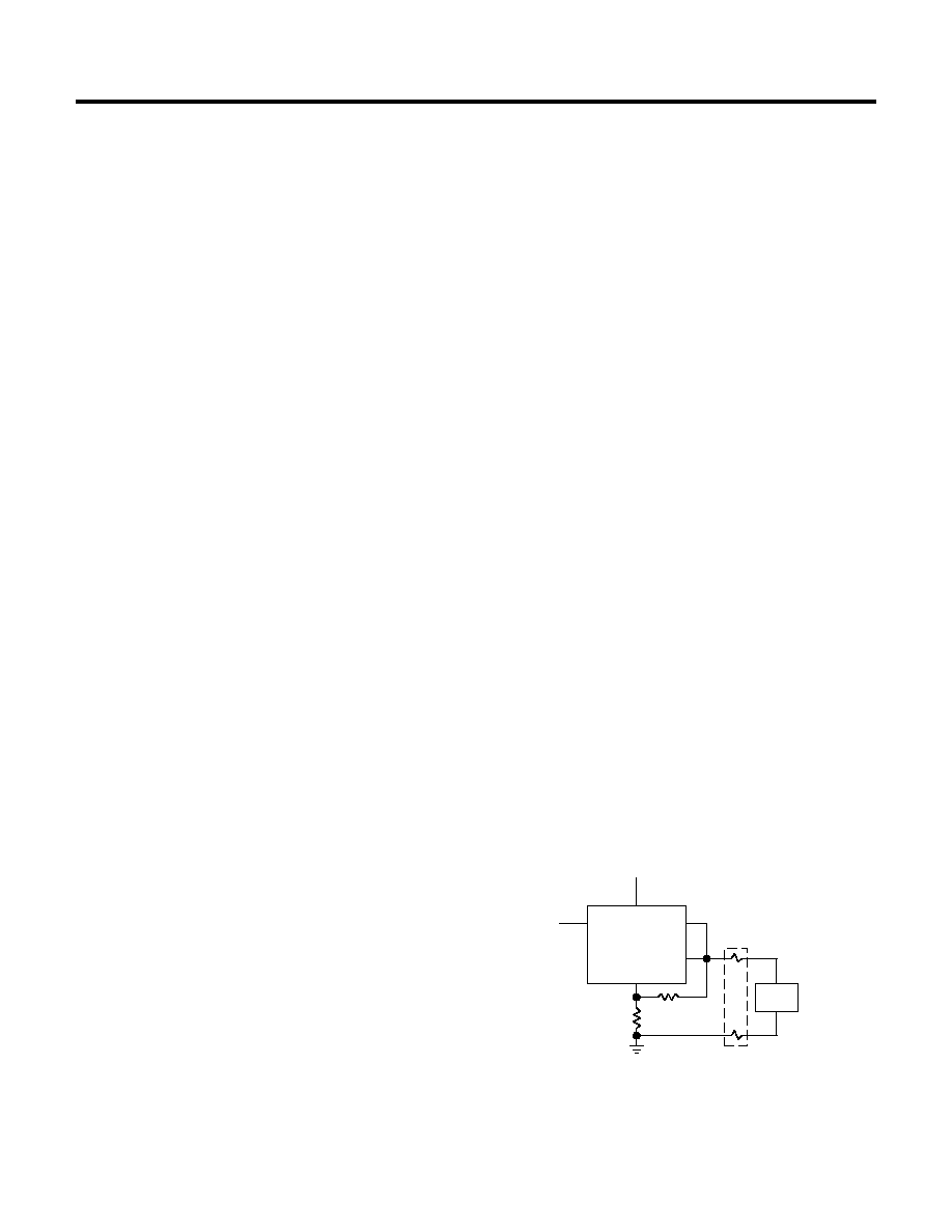
Grounding and Output Sensing
The AMS1508 allows true Kelvin sensing for both the high and
low side of the load. As a result the voltage regulation at he load
can be easily optimized. Voltage drops due to parasitic
resistances between the regulator and the load can be placed
inside the regulation loop of the AMS1508. The advantages of
remote sensing are illustrated in figures 1 through 3.
Figure 1 shows the device connected as a conventional 3 terminal
regulator with the Sense lead connected directly to the output of
the device. R
P
is the parasitic resistance of the connections
between the device and the load. Typically the load is a
microprocessor and R
P
is made up of the PC traces and /or
connector resistances (in the case of a modular regulator)
between the regulator and the processor. Trace A of figure 3
illustrates the effect of RP. Very small resistances cause
significant load regulation steps.
Figure 2 shows the device connected to take advantage of the
remote sense feature. The Sense pin and the top of the resistor
divider are connected to the top of the load; the bottom of the
resistor divider is connected to the bottom of the load. R
P
is now
connected inside the regulation loop of the AMS1508 and for
reasonable values of R
P
the load regulation at the load will be
negligible. The effect on output regulation can be seen in trace B
of figure 3.
CONTROL
POWER SENSE
AMS1508
OUTPUT
ADJ
LOAD
+
-
V
OUT
R
P
R
P
R1
R2
5V
3.3V
Figure 1. Conventional Load Sensing
Advanced Monolithic Systems, Inc. 6680B Sierra Lane, Dublin, CA 94568 Phone (925) 556-9090 Fax (925) 556-9140
AMS1508
APPLICATION HINTS
CONTROL
POWER SENSE
AMS1508
OUTPUT
ADJ
LOAD
+
-
V
OUT
R
P
R
P
R1
R2
5V
3.3V
Figure 2. Remote Load Sensing
(
I
OUT
)(R
P
)
TIME
V
OUT
FIGURE 1
V
OUT
FIGURE 2
I
OUT
Figure 3. Remote Sensing Improves Load Regulation
Voltage drops due to R
P
are not eliminated; they will add to the
dropout voltage of the regulator regardless of whether they are
inside or outside the regulation loop. The AMS1508 can control
the voltage at the load as long as the input-output voltage is
greater than the total of the dropout voltage of the device plus the
voltage drop across R
P
.
Stability
The circuit design used in the AMS1508 series requires the use of
an output capacitor as part of the device frequency compensation.
The addition of
150
µ
F aluminum electrolytic or a 22
µ
F solid
tantalum on the output will ensure stability for all operating
conditions. For best frequency response use capacitors with an
ESR of less than 1
.
In order to meet the transient requirements of the processor larger
value capacitors are needed. Tight voltage tolerances are required
in the power supply. To limit the high frequency noise generated
by the processor high quality bypass capacitors must be used. In
order to limit parasitic inductance (ESL) and resistance (ESR) in
the capacitors to acceptable limits, multiple small ceramic
capacitors in addition to high quality solid tantalum capacitors are
required.
When the adjustment terminal is bypassed to improve the ripple
rejection, the requirement for an output capacitor increases. The
Adjust pin is brought out on the fixed voltage device specifically
to allow this capability. To ensure good transient response with
heavy load current changes capacitor values on the order of
100
µ
F are used in the output of many regulators. To further
improve stability and transient response of these devices larger
values of output capacitor can be used.
The modern processors generate large high frequency current
transients. The load current step contains higher order frequency
components than the output coupling network must handle until
the regulator throttles to the load current level. Because they
contain parasitic resistance and inductance, capacitors are not
ideal elements. These parasitic elements dominate the change in
output voltage at the beginning of a transient load step change.
The ESR of the output capacitors produces an instantaneous step
in output voltage (
V=
I)(ESR). The ESL of the output
capacitors produces a droop proportional to the rate of change of
the output current (V= L)(
I/
t). The output capacitance
produces a change in output voltage proportional to the time until
the regulator can respond (
V=
t) (
I/C). Figure 4 illustrates
these transient effects.
CAPACITANCE
EFFECTS
ESR
EFFECTS
ESL
EFFECTS
POINT AT WHICH REGULATOR
TAKES CONTROL
SLOPE, V/t =
I/C
Figure 4.
Output Voltage
The AMS1508 series develops a 1.25V reference voltage
between the Sense pin and the Adjust pin (Figure5). Placing a
resistor between these two terminals causes a constant current to
flow through R1 and down through R2 to set the overall output
voltage. In general R1 is chosen so that this current is the
specified minimum load current of 10mA.The current out of the
Adjust pin is small, typically 50
µ
A and it adds to the current
from R1. Because I
ADJ
is very small it needs to be considered
only when very precise output voltage setting is required. For
best regulation the top of the resistor divider should be connected
directly to the Sense pin.
CONTROL
POWER OUTPUT
AMS1508
SENSE
ADJ
R1
R2
V
OUT
V
REF
V
POWER
I
ADJ
50
µ
A
+
+
+
V
CONTROL
V
OUT
= V
REF
(
1+ R2/R1)+I
ADJ
R2
Figure 5. Setting Output Voltage

Advanced Monolithic Systems, Inc. 6680B Sierra Lane, Dublin, CA 94568 Phone (925) 556-9090 Fax (925) 556-9140
AMS1508
APPLICATION HINTS
Protection Diodes
Unlike older regulators, the AMS1508 family does not need any
protection diodes between the adjustment pin and the output and
from the output to the input to prevent die over-stress. Internal
resistors are limiting the internal current paths on the AMS1508
adjustment pin, therefore even with bypass capacitors on the
adjust pin no protection diode is needed to ensure device safety
under short-circuit conditions. The Adjust pin can be driven on a
transient basis
±
7V with respect to the output without any device
degradation.
Diodes between the Output pin and V
POWER
pin are not usually
needed. Microsecond surge currents of 50A to 100A can be
handled by the internal diode between the Output pin and V
POWER
pin of the device. In normal operations it is difficult to get those
values of surge currents even with the use of large output
capacitances. If high value output capacitors are used, such as
1000
µ
F to 5000
µ
F and the V
POWER
pin is instantaneously shorted
to ground, damage can occur. A diode from output to input is
recommended, when a crowbar circuit at the input of the
AMS1508 is used (Figure 6). Normal power supply cycling or
even plugging and unplugging in the system will not generate
current large enough to do any damage.
CONTROL
POWER OUTPUT
AMS1508
SENSE
ADJ
R1
R2
V
OUT
V
POWER
+
+
+
D2*
D1*
V
CONTROL
Figure 6. Optional Clamp Diodes Protect Against
Input Crowbar Circuits
If the AMS1508 is connected as a single supply device with the
control and power input pins shorted together the internal diode
between the output and the power input pin will protect the
control input pin. As with any IC regulator, none the protection
circuitry will be functional and the internal transistors will break
down if the maximum input to output voltage differential is
exceeded.
Thermal Considerations
The AMS1508 series have internal power and thermal limiting
circuitry designed to protect the device under overload conditions.
However maximum junction temperature ratings should not be
exceeded under continuous normal load conditions. Careful
consideration must be given to all sources of thermal resistance
from junction to ambient, including junction-to-case, case-to-heat
sink interface and heat sink resistance itself.
Thermal resistance specification for both the Control Section and
the Power Transistor are given in the electrical characteristics.
The thermal resistance of the Control section is given as
0.65
∞
C/W and junction temperature of the Control section can
run up to 125
∞
C. The thermal resistance of the Power section is
given as 2.7
∞
C/W and junction temperature of the Power section
can run up to 150
∞
C. Due to the thermal gradients between the
power transistor and the control circuitry there is a significant
difference in thermal resistance between the Control and Power
sections.
Virtually all the power dissipated by the device is dissipated in
the power transistor. The temperature rise in the power transistor
will be greater than the temperature rise in the Control section
making the thermal resistance lower in the Control section. At
power levels below 12W the temperature gradient will be less
than 25
∞
C and the maximum ambient temperature will be
determined by the junction temperature of the Control section.
This is due to the lower maximum junction temperature in the
Control section. At power levels above 12W the temperature
gradient will be greater than 25
∞
C and the maximum ambient
temperature will be determined by the Power section. In both
cases the junction temperature is determined by the total power
dissipated in the device. For most low dropout applications the
power dissipation will be less than 12W.
The power in the device is made up of two components: the
power in the output transistor and the power in the drive circuit.
The power in the control circuit is negligible.
The power in the drive circuit is equal to:
P
DRIVE
= (V
CONTROL
- V
OUT
)(I
CONTROL
)
where I
CONTROL
is equal to between I
OUT
/100(typ) and
I
OUT
/58(max).
The power in the output transistor is equal to:
P
OUTPUT
= (V
POWER
-V
OUT
)(I
OUT
)
The total power is equal to:
P
TOTAL
= P
DRIVE
+ P
OUTPUT
Junction-to-case thermal resistance is specified from the IC
junction to the bottom of the case directly below the die. This is
the lowest resistance path for the heat flow. In order to ensure the
best possible thermal flow from this area of the package to the
heat sink proper mounting is required. Thermal compound at the
case-to-heat sink interface is recommended. A thermally
conductive spacer can be used, if the case of the device must be
electrically isolated, but its added contribution to thermal
resistance has to be considered.

Advanced Monolithic Systems, Inc. 6680B Sierra Lane, Dublin, CA 94568 Phone (925) 556-9090 Fax (925) 556-9140
AMS1508
TYPICAL PERFORMANCE CHARACTERISTICS
Reference Voltage vs
Temperature
1.242
1.244
1.246
1.248
1.250
1.252
1.254
1.256
1.258
-50 -25
0
25
50
75 100 125 150
REFERENCE VOLTAGE (V)
TEMPERATURE (∞ C)
Load Current Step Response
50
µ
/DIV
V
OUT
50
µ
V/DIV
7A
400mA
LOAD
0
1
2
3
4
5
6
7
0
1
2
3
4
5
6
7
0
1
2
3
4
5
6
7
0
20
40
60
80
100
120
140
CONTROL PIN CURRENT (mA)
0
2
1
MINMUM CONTROL VOLTAGE
(V
CONTROL
- V
OUT
)(V)
0
0.5
1.0
MINIMUM POWER VOLTAGE
OUTPUT CURRENT (A)
OUTPUT CURRENT (A)
OUTPUT CURRENT (A)
Control Pin Current vs
Output Current
Minimum Control Voltage
Dropout Voltage -
Minimum Power Voltage
TYPICAL
DEVICE
T
J
= 125∞ C
T
J
= 25∞ C
8
8
T
J
= 25∞ C
T
J
= 125∞ C
8

Advanced Monolithic Systems, Inc. 6680B Sierra Lane, Dublin, CA 94568 Phone (925) 556-9090 Fax (925) 556-9140
AMS1508
PACKAGE DIMENSIONS inches (millimeters) unless otherwise noted.
5 LEAD TO-220 PLASTIC PACKAGE (T)
5 LEAD TO-263 PLASTIC PACKAGE (M)
0.060
(1.524)
TYP
0.390-0.415
(9.906-10.541)
0.330-0.370
(8.382-9.398)
0.057-0.077
(1.447-1.955)
0.165-0.180
(4.191-4.572)
0.045-0.055
(1.143-1.397)
0.095-0.115
(2.413-2.921)
0.90-0.110
(2.29-2.79)
0.013-0.023
(0.330-0.584)
0.108
(2.74)
TYP
(
0.102
)
+0.203
-0.102
0.004 +0.008
-0.004
M (DD5) AMS DRW#042192R1
(5.05-5.54 )
0.199-0.218
0.032
(0.81)
TYP
0.335-0.345
(8.51-8.77)
0.387-0.413
(9.83-10.49)
0.170-0.190
(4.32-4.82)
0.045-0.055
(1.143-1.397)
0.105
(2.67)
0.013-0.023
(0.330-0.584)
T (TO-220 ) AMS DRW# 042194
0.149-0.153
(3.77-3.87)
DIA
0.240-0.260
(6.100-6.600)
0.032
(0.81)
TYP
TYP
0.062-0.072
(1.570-1.830)
0.460-0.500
(11.684-12.700)
0.520-0.570
(13.208-14.478)
0.980-1.070
(24.892-27.178)
0.575-0.605
(14.61-15.37)

Advanced Monolithic Systems, Inc. 6680B Sierra Lane, Dublin, CA 94568 Phone (925) 556-9090 Fax (925) 556-9140
AMS1508
PACKAGE DIMENSIONS inches (millimeters) unless otherwise noted
(Continued).
7 LEAD TO-220 PLASTIC PACKAGE (T)
0.330-0.370
(8.382-9.398)
0.040-0.060
(1.016-1.524)
0.390-0.415
(9.906-10.541)
0.165-0.180
(4.191-4.572)
0.045-0.055
(1.143-1.397)
0.095-0.115
(2.413-2.921)
0.013-0.023
(0.330-0.584)
T (TO-220 ) AMS DRW# 042291
0.147-0.155
(3.734-3.937)
DIA
0.230-0.270
(5.842-6.858)
0.460-0.500
(11.684-12.700)
0.570-0.620
(14.478-15.748)
0.520-0.620
(13.208-14.224)
0.980-1.070
(24.892-27.178)
0.026-0.036
(0.660-0.914)