Advanced Monolithic Systems, Inc. 6680B Sierra Lane, Dublin, CA 94568 Phone (925) 556-9090 Fax (925) 556-9140
Advanced
AMS2954
Monolithic
250mA LOW DROPOUT VOLTAGE REGULATOR
Systems
FEATURES
APPLICATIONS
∑
∑
2.5V, 3.0V, 3.3V and 5.0V Versions
∑
∑
Battery Powered Systems
∑
∑
High Accuracy Output Voltage
∑
∑
Portable Consumer Equipment
∑
∑
Extremely Low Quiescent Current
∑
∑
Cordless Telephones
∑
∑
Low Dropout Voltage
∑
∑
Portable (Notebook) Computers
∑
∑
Extremely Tight Load and Line Regulation
∑
∑
Portable Instrumentation
∑
∑
Very Low Temperature Coefficient
∑
∑
Radio Control Systems
∑
∑
Current and Thermal Limiting
∑
∑
Automotive Electronics
∑
∑
Needs Minimum Capacitance (1
µ
µ
F) for Stability
∑
∑
Avionics
∑
∑
Unregulated DC Positive Transients 60V
∑
∑
Low-Power Voltage Reference
ADDITIONAL FEATURES (ADJ ONLY)
∑
∑
1.24V to 29V Programmable Output
∑
∑
Error Flag Warning of Voltage Output Dropout
∑
∑
Logic Controlled Electronic Shutdown
GENERAL DESCRIPTION
The AMS2954 series are micropower voltage regulators ideally suited for use in battery-powered systems. These devices
feature very low quiescent current (typ.75µA), and very low dropout voltage (typ.50mV at light loads and 380mV at 250mA)
thus prolonging battery life. The quiescent current increases only slightly in dropout. The AMS2954 has positive transient
protection up to 60V and can survive unregulated input transient up to 20V below ground. The AMS2954 was designed to
include a tight initial tolerance (typ. 0.5%), excellent load and line regulation (typ. 0.05%), and a very low output voltage
temperature coefficient, making these devices useful as a low-power voltage reference.
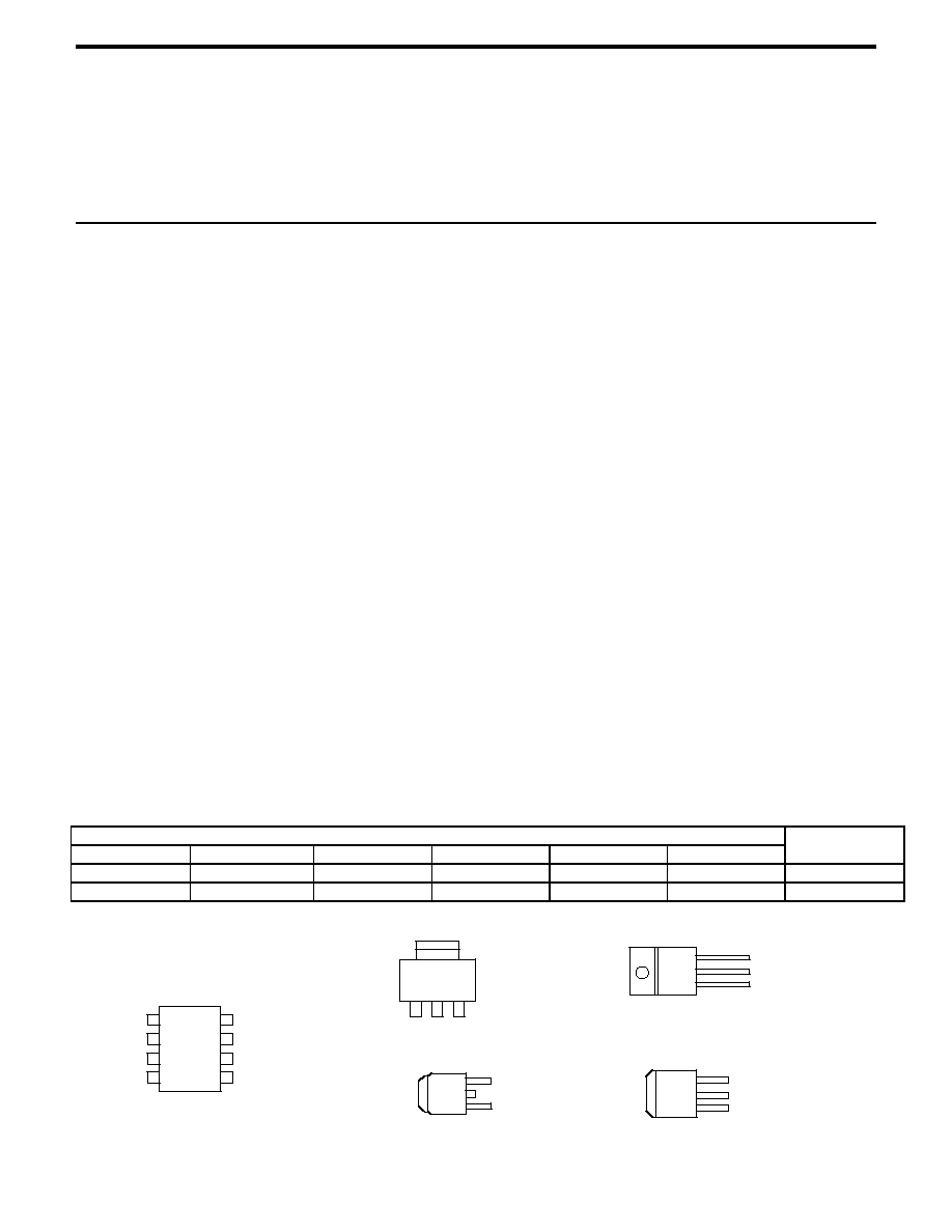
The AMS2954 is available in the 3L TO-220 package, 3L TO-263, SOT-223, TO-252 and in 8-pin plastic SOIC and DIP
packages. In the 8L SOIC and PDIP packages the following additional features are offered: an error flag output warns of a low
output voltage, often due to failing batteries on input; the logic-compatible shutdown input enables the regulator to be switched
on and off; the device may be pin-strapped for a, 2.5, 3.0V, 3.3V or 5V output, or programmed from 1.24V to 29V with an
external pair of resistors.
ORDERING INFORMATION
PACKAGE TYPE
OPERATING
3 LEAD TO-220
3 LEAD TO-263
TO-252
SOT-223
8 LEAD SOIC
8 LEAD PDIP
TEMP. RANGE
AMS2954ACT-X AMS2954ACM-X AMS2954ACD-X AMS2954AC-X AMS2954ACS-X AMS2954CP-X
IND.
AMS2954CT-X
AMS2954CM-X
AMS2954CD-X
AMS2954C-X
AMS2954CS-X
AMS2954CP-X
IND
X = 2.5V, 3.0V, 3.3V, 5.0V
PIN CONNECTIONS
8L SOIC/ 8L PDIP
1
2
8
4
3
7
5
6 V
TAP
ERROR
FEEDBACK
OUTPUT
SENSE
SHUTDOWN
INPUT
GROUND
Top View
TAB IS
GND
TO-252 FRONT VIEW
1
2
3
1
2
3
TAB IS
GND
1
2
3
TAB IS
GND
3L TO-263 FRONT VIEW
OUTPUT
INPUT
OUTPUT
OUTPUT
INPUT
INPUT
3L TO-220 FRONT VIEW
SOT-223 TOP VIEW
INPUT GND
OUTPUT
GND
GND
1
2
3

Advanced Monolithic Systems, Inc. 6680B Sierra Lane, Dublin, CA 94568 Phone (925) 556-9090 Fax (925) 556-9140
AMS2954
ABSOLUTE MAXIMUM RATINGS
(Note 1)
Input Supply Voltage
-0.3 to +30V
Soldering Dwell Time, Temperature
SHUTDOWN Input Voltage,
Wave
4 seconds, 260
∞
C
Error Comparator Output
Infrared
4 seconds, 240
∞
C
Voltage,(Note 9)
Vapor Phase
4 seconds, 219
∞
C
FEEDBACK Input Voltage
-1.5 to +30V
(Note 9) (Note 10)
OPERATING RATINGS
(Note 1)
Power Dissipation
Internally Limited
Junction Temperature
+150
∞
C
Max. Input Supply Voltage
40V
Storage Temperature
-65
∞
C to +150
∞
C
Junction Temperature Range
ESD
2kV
(T
J
) (Note 8)
AMS2954AC-X
AMS2954C-X
-40
∞
C to +125
∞
C
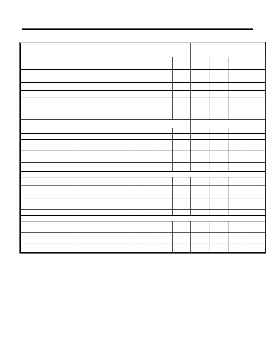
ELECTRICAL CHARACTERISTICS
at Vs=Vout+1V, Ta=25∞C, unless otherwise noted
.
Parameter
Conditions
(Note 2)
AMS2954AC
Min. Typ. Max.
AMS2954C
Min. Typ. Max.
Units
2.5 V Versions (Note 16)
Output Voltage
TJ = 25∞C (Note 3)
-25∞C
TJ
85∞C
Full Operating Temperature
Range
2.488
2.475
2.470
2.5
2.5
2.5
2.512
2.525
2.530
2.475
2.450
2.440
2.5
2.5
2.5
2.525
2.550
2.560
V
V
V
Output Voltage
100
µ
A
IL
250 mA
TJ
TJMAX
2.463
2.5
2.537
2.448
2.5
2.562
V
3.0 V Versions (Note 16)
Output Voltage
TJ = 25∞C (Note 3)
-25∞C
TJ
85∞C
Full Operating Temperature
Range
2.985
2.970
2.964
3.0
3.0
3.0
3.015
3.030
3.036
2.970
2.955
2.940
3.0
3.0
3.0
3.030
3.045
3.060
V
V
V
Output Voltage
100
µ
A
IL
250 mA
TJ
TJMAX
2.958
3.0
3.042
2.928
3.0
3.072
V
3.3 V Versions (Note 16)
Output Voltage
TJ = 25∞C (Note 3)
-25∞C
TJ
85∞C
Full Operating Temperature
Range
3.284
3.267
3.260
3.3
3.3
3.3
3.317
3.333
3.340
3.267
3.251
3.234
3.3
3.3
3.3
3.333
3.350
3.366
V
V
V
Output Voltage
100
µ
A
IL
250 mA
TJ
TJMAX
3.254
3.3
3.346
3.221
3.3
3.379
V
5 V Versions (Note 16)
Output Voltage
TJ = 25∞C (Note 3)
-25∞C
TJ
85∞C
Full Operating Temperature
Range
4.975
4.95
4.94
5.0
5.0
5.0
5.025
5.050
5.06
4.95
4.925
4.90
5.0
5.0
5.0
5.05
5.075
5.10
V
V
V
Output Voltage
100
µ
A
IL
250 mA
TJ
TJMAX
4.925
5.0
5.075
4.88
5.0
5.12
V
All Voltage Options
Output Voltage
Temperature Coefficient
(Note 12) (Note 4)
20
100
50
150
ppm/∞C
Line Regulation (Note 14)
6V
Vin
30V (Note 15)
0.03
0.1
0.04
0.2
%
Load Regulation (Note 14)
100
µ
A
IL
250 mA
0.04
0.16
0.1
0.2
%
Advanced Monolithic Systems, Inc. 6680B Sierra Lane, Dublin, CA 94568 Phone (925) 556-9090 Fax (925) 556-9140
AMS2954
ELECTRICAL CHARACTERISTICS
(Note 2) (Continued)
PARAMETER
CONDITIONS
(Note 2)
AMS2954AC
Min. Typ. Max.
AMS2954C
Min. Typ. Max.
Units
Dropout Voltage
(Note 5)
IL = 100
µ
A
IL = 250 mA
50
380
80
600
50
380
80
600
mV
mV
Ground Current
IL = 100
µ
A
IL = 250 mA
75
15
120
20
75
15
120
20
µ
A
mA
Current Limit
Vout = 0
200
500
200
500
mA
Thermal Regulation
(Note 13)
0.05
0.2
0.05
0.2
%/W
Output Noise,
10Hz to 100KHz
CL = 1
µ
F
CL = 200
µ
F
CL = 13.3
µ
F
(Bypass = 0.01
µ
F pins 7 to 1)
430
160
100
430
160
100
µ
V rms
µ
V rms
µ
V rms
8-Pin Versions only
AMS2954AC
AMS2954C
Reference Voltage
1.22
1.235
1.25
1.21
1.235
1.26
V
Reference Voltage
Over Temperature (Note 7)
1.19
1.27
1.185
1.285
V
Feedback Pin Bias Current
40
60
40
60
nA
Reference Voltage Temperature
Coefficient
( Note 12 )
20
50
ppm/∞C
Feedback Pin Bias Current
Temperature Coefficient
0.1
0.1
nA/∞C
Error Comparator
Output Leakage Current
V
OH
= 30V
0.01
1
0.01
1
µ
A
Output Low Voltage
Vin = 4.5V
IOL = 400
µ
A
150
250
150
250
mV
Upper Threshold Voltage
(Note 6)
40
60
40
60
mV
Lower Threshold Voltage
(Note 6)
75
95
75
95
mV
Hysteresis
(Note 6)
15
15
mV
Shutdown Input
Input logic Voltage
Low (Regulator ON)
High (Regulator OFF)
2
1.3
0.7
2
1.3
0.7
V
V
Shutdown Pin Input Current
(Note 3)
Vs = 2.4V
Vs = 30V
30
450
50
600
30
450
50
600
µ
A
µ
A
Regulator Output Current in
Shutdown (Note 3)
(Note 11)
3
10
3
10
µ
A
Note 1: Absolute Maximum Ratings are limits beyond which damage to the device may occur. Operating Ratings are conditions under which operation of the
device is guaranteed. Operating Ratings do not imply guaranteed performance limits. For guaranteed performance limits and associated test conditions, see the
Electrical Characteristics tables.
Note 2: Unless otherwise specified all limits guaranteed for V
IN
= (
V
ONOM
+1)V, I
L
= 100
µ
A and C
L
= 1
µ
F for 5V versions and 2.2
µ
F for 3V and 3.3V
versions. Limits appearing in boldface type apply over the entire junction temperature range for operation. Limits appearing in normal type apply for T
A
= T
J
=
25
∞
C Additional conditions for the 8-pin versions are FEEDBACK tied to V
TAP
, OUTPUT tied to SENSE and V
SHUTDOWN
0.8V.
Note 3: Guaranteed and 100% production tested.
Note 4: Guaranteed but not 100% production tested. These limits are not used to calculate outgoing AQL levels.
Note 5: Dropout voltage is defined as the input to output differential at which the output voltage drops 100 mV below its nominal value measured at 1V
differential. At very low values of programmed output voltage, the minimum input supply voltage of 2V ( 2.3V over temperature) must be taken into account.
Note 6: Comparator thresholds are expressed in terms of a voltage differential at the feedback terminal below the nominal reference voltage measured at
V
IN
= (
V
ONOM
+1)V. To express these thresholds in terms of output voltage change, multiply by the error amplifier gain = Vout/Vref = (R1 + R2)/R2. For
example, at a programmed output voltage of 5V, the error output is guaranteed to go low when the output drops by 95 mV x 5V/1.235 = 384 mV. Thresholds
remain constant as a percent of V
out
as V
out
is varied, with the dropout warning occurring at typically 5% below nominal, 7.5% guaranteed.
Note 7: V
ref
V
out
(V
in
- 1V), 2.3
V
in
30V, 100
µ
A
I
L
250 mA, T
J
T
JMAX
.
Advanced Monolithic Systems, Inc. 6680B Sierra Lane, Dublin, CA 94568 Phone (925) 556-9090 Fax (925) 556-9140
AMS2954
Note 8: The junction-to-ambient thermal resistance are as follows:60
∞
C/W for the TO-220 (T), 73
∞
C/W for the TO-263 (M), 80
∞
C/W for the TO-252 (D),
90
∞
C/W for the SOT-223 (with package soldering to copper area over backside ground plane or internal power plane
JA
can vary from 46
∞
C/W to
>
90
∞
C/W
depending on mounting technique and the size of the copper area), 105
∞
C/W for the molded plastic DIP (P) and 160
∞
C/W for the molded plastic SO-8 (S).
Note 9: May exceed input supply voltage.
Note 10: When used in dual-supply systems where the output terminal sees loads returned to a negative supply, the output voltage should be diode-clamped to
ground.
Note 11: V
shutdown
2V, V
in
30V, V
out
=0, Feedback pin tied to 5V
TAP
.
Note 12: Output or reference voltage temperature coefficients defined as the worst case voltage change divided by the total temperature range.
Note 13: Thermal regulation is defined as the change in output voltage at a time T after a change in power dissipation is applied, excluding load or line
regulation effects. Specifications are for a 50mA load pulse at V
IN
=30V (1.25W pulse) for T =10 ms.
Note 14: Regulation is measured at constant junction temperature, using pulse testing with a low duty cycle. Changes in output voltage due to heating effects
are covered under the specification for thermal regulation.
Note 15: Line regulation for the AMS2954 is tested at 150
∞
C for I
L
= 1 mA. For I
L
= 100
µ
A and T
J
= 125
∞
C, line regulation is guaranteed by design to 0.2%.
See typical performance characteristics for line regulation versus temperature and load current.
BLOCK DIAGRAM AND TYPICAL APPLICATIONS
AMS2954-XX
3 Lead Packages
AMS2954-XX
8 Lead Packages
INPUT
OUTPUT
GROUND
ERROR
AMPLIFIER
1.23V
REFERENCE
UNREGULATED DC
V
OUT
I
L
150mA
SEE APPLICATION
HINTS
+
+
+
+
-
INPUT
OUTPUT
GROUND
ERROR
AMPLIFIER
1.23V
REFERENCE
UNREGULATED DC
V
OUT
I
L
150mA
SEE APPLICATION
HINTS
+
+
+
+
-
FEED-
BACK
SHUT-
DOWN
SENSE
V
TAP
ERROR
TO CMOS
OR TTL
+
-
+
330k
4
5
6
2
1
8
7
3
FROM
CMOS
OR TTL
50mV
ERROR DETECTION COMPARATOR
Advanced Monolithic Systems, Inc. 6680B Sierra Lane, Dublin, CA 94568 Phone (925) 556-9090 Fax (925) 556-9140
AMS2954
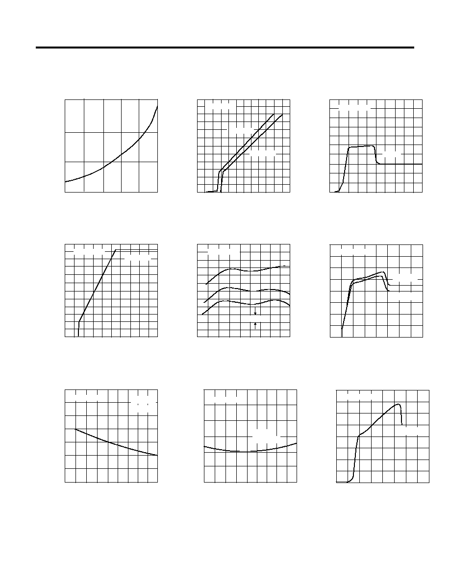
TYPICAL PERFORMANCE CHARACTERISTICS
0
40
100
60
160
0
1
2
3
4
5
6
7
8
INPUT VOLTAGE (V)
Quiescent Current
QUIESCENT CURRENT (
µ
A)
125
250
Input Current
25
50
75
100
150
175
200
225
INPUT VOLTAGE (V)
INPUT CURRENT (
µ
A)
5V OUTPUT
-75
0
25 50 75 100 125
5.06
5.0
150
OUTPUT VOLTAGE (V)
Temperature Drift of 3
Representative Units
TEMPERATURE (∞ C)
5.04
4.98
4.94
-50 -25
1
50
100
250
LOAD CURRENT (mA)
GROUND CURRENT (mA)
0.1
1
10
20
Quiescent Current
Dropout Characteristics
INPUT VOLTAGE (V)
OUTPUT VOLTAGE (V)
I
O
=1mA
0
90
270
Input Current
15
30
45
75
120
150
180
210
INPUT VOLTAGE (V)
INPUT CURRENT (mA)
-75
0
25 50 75 100 125
120
90
150
QUIESCENT CURRENT (
µ
A)
Quiescent Current
TEMPERATURE (∞ C)
100
70
60
-50 -25
I
L
= 100
µ
A
-75
0
25 50 75 100 125
35
150
QUIESCENT CURRENT (mA)
Quiescent Current
TEMPERATURE (∞ C)
25
15
5
-50 -25
I
L
= 250mA
50
80
110
20
80
140
120
0
6
15
9
24
0
1
2
3
4
5
6
7
8
INPUT VOLTAGE (V)
Quiescent Current
QUIESCENT CURRENT (
mA)
3
12
21
18
0
1
2
3
4
5
6
1
2
3
4
5
6
7
8
9 10
0
0
1
2
3
4
5
6
0
1
2
3
4
5
6
7
8
9 10
0
60
240
5.02
4.96
5V OUTPUT
5V OUTPUT
5V OUTPUT
5V OUTPUT
5V OUTPUT
5V OUTPUT
5V OUTPUT
I
L
= 1 mA
I
L
= 250mA
I
O
=250mA
I
L
= 0mA
V
IN
= 6V
V
IN
= 6V
I
O
=250mA
0.2%
R
L
=
30
20
10
150
200
Advanced Monolithic Systems, Inc. 6680B Sierra Lane, Dublin, CA 94568 Phone (925) 556-9090 Fax (925) 556-9140
AMS2954
TYPICAL PERFORMANCE CHARACTERISTICS
(Continued)
-75
0
25 50 75 100 125
450
300
150
SHORT CIRCUIT CURRENT (
m
A)
Short Circuit Current
TEMPERATURE (∞ C)
350
200
150
-50 -25
-75
0
25 50 75 100 125
600
150
DROPOUT VOLTAGE (mV)
Dropout Voltage
TEMPERATURE (∞ C)
400
100
0
-50 -25
I
L
= 250mA
100
250
400
-75
0
25 50 75 100 125
2.2
150
MINIMUM OPERATING VOLTAGE (V)
AMS2954 Minimum Operating Voltage
TEMPERATURE (∞ C)
-50 -25
-75
0
25 50 75 100 125
20
150
BIAS CURRENT (nA)
AMS2954 Feedback Bias Current
TEMPERATURE (∞ C)
0
-30
-50 -25
-2.0
-1.5 -1.0
-0.5
0
0.5
-250
50
-50
-150
AMS2954 Feedback Pin Current
1.0
FEEDBACK VOLTAGE (V)
FEEDBACK CURRENT (
µ
A)
-200
0
-100
200
400
600
100
mV
800
INPUT
VOLTAGE
Line Transient Response
TIME (
µ
s)
0
8V
4V
0
I
L
= 1mA
V
OUT
= 5V
0.0
0.3 0.4 0.5 0.6 0.7 0.8
2.5
0.9
SINK CURRENT (mA)
AMS2954 Comparator Sink Current
OUTPUT LOW VOLTAGE (V)
1.5
0.0
0.1 0.2
0
3
4
5
6
7
8
9
4
ERROR OUTPUT (V)
AMS2954 Error Comparator Output
INPUT VOLTAGE (V)
5
2
1
1
2
0
3
6
V
OUT
= 5V
100
µ
A
10mA
100mA
250mA
OUTPUT CURRENT
DROPOUT VOLTAGE (mV)
0
500
Dropout Voltage
500
300
50
400
300
200
100
2.1
2.0
1.9
1.8
1.7
1.6
10
-10
-20
50
mV
-50
mV
6V
OUTPUT VOLTAGE
CHANGE
~
~
~
~
8
7
2.0
1.0
0.5
I
L
= 100
µ
A
T
J
= 25∞C
T
A
= 125∞C
T
A
=
25∞C
T
A
= -55∞C
PIN 7 DRVEN BY EXTERNAL
SOURCE (REGULATOR RUN
OPEN LOOP)
T
A
=
125∞C
T
A
=
25∞C
T
A
= -55∞C
C
L
= 1
µ
F
HYSTERESIS
50k RESISTOR TO
EXTERNAL 5V SUPPLY
50k
RESISTOR
TO V
OUT
Advanced Monolithic Systems, Inc. 6680B Sierra Lane, Dublin, CA 94568 Phone (925) 556-9090 Fax (925) 556-9140
AMS2954
TYPICAL PERFORMANCE CHARACTERISTICS
(Continued)
Load Transient Response
TIME (ms)
OUTPUT VOLTAGE
CHANGE (mV)
C
L
= 1
µ
F
0
1
2
3
4
5
100
0
50
150
250
V
OUT
= 5V
2
7
AMS2954 Enable Transient
0
2
0
1
3
4
5
6
TIME (
µ
s)
SHUTDOWN PIN
VOLTAGE (V)
0
100 200 300 400 500 600 700
-100
-2
I
L
= 10 mA
200
100
-50
-100
250
mA
µ
A
~
~
~
~
LOAD
CURRENT
Load Transient Response
TIME (ms)
OUTPUT VOLTAGE
CHANGE (mV)
0
4
8
12
16
20
100
-20
0
40
80
60
20
-40
-60
250
mA
µ
A
~
~
LOAD
CURRENT
OUTPUT
VOLTAGE (V)
C
L
= 10
µ
F
V
OUT
= 5V
V
OUT
= 5V
C
L
= 10
µ
F
C
L
= 1
µ
F
V
IN
= 8V
10
100
1K
100K
FREQUENCY (Hz)
OUPUT IMPEDANCE (
)
0.01
10
Output Impedance
2
1
0.05
0.02
10
1
10
4
10
5
90
60
10
6
RIPPLE REJECTION (dB)
Ripple Rejection
FREQUENCY (Hz)
70
40
30
10
2
I
L
= 100
µ
A
20
50
80
V
IN
= 6V
10
3
10
1
10
4
10
5
90
60
10
6
RIPPLE REJECTION (dB)
Ripple Rejection
FREQUENCY (Hz)
70
40
30
10
2
I
L
= 1mA
20
50
80
V
IN
= 6V
10
3
10
1
10
4
10
5
80
50
10
6
RIPPLE REJECTION (dB)
Ripple Rejection
FREQUENCY (Hz)
60
30
20
10
2
I
L
= 50mA
10
40
70
V
IN
= 6V
10
3
FREQUENCY (Hz)
VOLTAGE NOISE SPECTRAL
DENSITY(mV/
Hz)
0.0
3.5
AMS2954 Output Noise
2.0
1.5
0.5
10
4
10
5
10
2
10
3
1.0
3.0
2.5
-75
0
25 50 75 100 125
400
200
150
PIN 2 TO PIN 4 RESISTANCE (k
)
AMS2954 Divider Resistance
TEMPERATURE (∞ C)
300
100
-50 -25
0
5
0.1
0.2
0.5
10K
1M
C
L
= 1
µ
F
I
L
= 250mA
C
L
= 220
µ
F
C
L
= 3.3
µ
F
0.01
µ
F
BYPASS
PIN 1 TO
PIN 7
5V
OUTPUT
I
L
= 250mA
C
L
= 1
µ
F
V
OUT
= 5V
C
L
= 1
µ
F
V
OUT
= 5V
I
O
= 1 mA
I
O
= 100
µ
A
I
O
= 250mA
V
OUT
= 5V
C
L
= 1
µ
F
I
L
= 0
V
OUT
= 5V
C
L
= 1
µ
F
I
L
= 10mA

Advanced Monolithic Systems, Inc. 6680B Sierra Lane, Dublin, CA 94568 Phone (925) 556-9090 Fax (925) 556-9140
AMS2954
TYPICAL PERFORMANCE CHARACTERISTICS
(Continued)
-75
0
25 50 75 100 125
1.8
1.2
150
SHUTDOWN TRESHOLD VOLTAGE (V)
Shutdown Treshold Voltage
TEMPERATURE (∞ C)
1.6
1.0
0.6
-50 -25
1.4
0.8
REGULATOR OFF
0
5
10
15
20
25
0
300
200
100
AMS2954 Maximum Rated
Output Current
30
INPUT VOLTAGE (V)
OUTPUT CURRENT (
m
A)
50
250
150
0
5
Thermal Response
0
1
-2
2
4
TIME (
µ
s)
POWER
DISSIPATION (W)
10
20
30
40
50
0
-1
5
15
20
25
30
0
30
OUTPUT VOLTAGE CHANGE (V)
Line Regulation
INPUT VOLTAGE (V)
10
-10
10
I
L
= 100
µ
A
10
-5
5
0
~
~
5
25
20
15
0
5
10
15
20
25
0
300
200
100
AMS2954 Maximum Rated
Output Current
30
INPUT VOLTAGE (V)
OUTPUT CURRENT (
m
A)
50
250
150
~
~
OUTPUT VOLTAGE
CHANGE (mV)
1.25W
T
A
= 25∞ C
T
A
= 50∞ C
T
A
= 25∞ C
T
A
= 85∞ C
T
A
= 85∞ C
T
JMAX
= 125∞ C
V
OUT
= 5V
8 PIN MOLDED
DIP SOLDERED
TO PC BOARD
REGULATOR ON
SOT-223 PACKAGE
SOLDERED TO PC
BOARD
T
JMAX
= 125∞ C
I
L
= 1mA
I
L
= 100
µ
A
T
J
= 150∞ C
T
J
= 125∞ C
Advanced Monolithic Systems, Inc. 6680B Sierra Lane, Dublin, CA 94568 Phone (925) 556-9090 Fax (925) 556-9140
AMS2954
APPLICATION HINTS
External Capacitors
A 1.0
µ
F or greater capacitor is required between output and
ground for stability at output voltages of 5V or more. At lower
output voltages, more capacitance is required (2.2
µ
or more is
recommended for 2.5V, 3.0V and 3.3V versions). Without this
capacitor the part will oscillate. Most types of tantalum or
aluminum electrolytic works fine here; even film types work but
are not recommended for reasons of cost. Many aluminum types
have electrolytes that freeze at about -30
∞
C, so solid tantalums are
recommended for operation below -25
∞
C. The important
parameters of the capacitor are an ESR of about 5
or less and
resonant frequency above 500 kHz parameters in the value of the
capacitor. The value of this capacitor may be increased without
limit.
At lower values of output current, less output capacitance is
required for stability. The capacitor can be reduced to 0.33
µ
F for
currents below 10 mA or 0.1
µ
F for currents below 1 mA. Using
the adjustable versions at voltages below 5V runs the error
amplifier at lower gains so that more output capacitance is needed.
For the worst-case situation of a 300mA load at 1.23V output
(Output shorted to Feedback) a 3.3
µ
F (or greater) capacitor should
be used.
Unlike many other regulators, the AMS2954, will remain stable
and in regulation with no load in addition to the internal voltage
divider. This is especially important in CMOS RAM keep-alive
applications. When setting the output voltage of the AMS2954
version with external resistors, a minimum load of 1
µ
A is
recommended.
A 1
µ
F tantalum or aluminum electrolytic capacitor should be
placed from the AMS2954/AMS2954 input to the ground if there
is more than 10 inches of wire between the input and the AC filter
capacitor or if a battery is used as the input.
Stray capacitance to the AMS2954 Feedback terminal can cause
instability. This may especially be a problem when using a higher
value of external resistors to set the output voltage. Adding a 100
pF capacitor between Output and Feedback and increasing the
output capacitor to at least 3.3
µ
F will fix this problem.
Error Detection Comparator Output
The comparator produces a logic low output whenever the
AMS2954 output falls out of regulation by more than
approximately 5%. This figure is the comparator's built-in offset
of about 60 mV divided by the 1.235 reference voltage (Refer to
the block diagram). This trip level remains "5% below normal"
regardless of the programmed output voltage of the 2951. For
example, the error flag trip level is typically 4.75V for a 5V output
or 11.4V for a 12V output. The out of regulation condition may be
due either to low input voltage, current limiting, or thermal
limiting.
Figure 1 gives a timing diagram depicting the ERROR signal and
the regulator output voltage as the AMS2954 input is ramped up
and down. For 5V versions the ERROR signal becomes valid
(low) at about 1.3V input. It goes high at about 5V input (the input
voltage at which Vout = 4.75 ).
Since the AMS2954's dropout voltage is load dependent (see
curve in typical performance characteristics), the input voltage trip
point (about 5V) will vary with the load current. The output
voltage trip point (approx. 4.75V) does not vary with load.
The error comparator has an open-collector output which requires
an external pull-up resistor. This resistor may be returned to the
output or some other supply voltage depending on system
requirements. In determining a value for this resistor, note that the
output is rated to sink 400
µ
A, this sink current adds to battery
drain in a low battery condition. Suggested values range from
100K to 1M
. The resistor is not required if this output is unused.
OUTPUT
VOLTAGE
ERROR*
INPUT
VOLTAGE
4.75V
5V
1.3V
FIGURE 1. ERROR Output Timing
*When
V
IN
1.3V the error flag pin becomes a high impedance,
and the error flag voltage rises to its pull-up voltage. Using V
out
as
the pull-up voltage (see Figure 2), rather than an external 5V
source, will keep the error flag voltage under 1.2V (typ.) in this
condition. The user may wish to drive down the error flag voltage
using equal value resistors (10 k suggested), to ensure a low-
level logic signal during any fault condition, while still allowing a
valid high logic level during normal operation.
Programming the Output Voltage
The AMS2954 may be pin-strapped for the nominal fixed output
voltage using its internal voltage divider by tying the output and
sense pins together, and also tying the feedback and V
TAP
pins
together. Alternatively, it may be programmed for any output
voltage between its 1.235V reference and its 30V maximum
rating. As seen in Figure 2, an external pair of resistors is
required.
The complete equation for the output voltage is:
V
out
= V
REF
◊
(1 + R
1
/ R
2
)+ I
FB
R
1
where V
REF
is the nominal 1.235 reference voltage and I
FB
is the
feedback pin bias current, nominally -20 nA. The minimum
recommended load current of 1
µ
A forces an upper limit of 1.2
M
on value of R
2
, if the regulator must work with no load (a
condition often found in CMOS in standby) I
FB
will produce a 2%
typical error in V
OUT
which may be eliminated at room
temperature by trimming R
1
. For better accuracy, choosing R2 =
100k reduces this error to 0.17% while increasing the resistor
program current by 12
µ
A. Since the AMS2954 typically draws 60
µ
A at no load with Pin 2 open-circuited, this is a small price to
pay.
Advanced Monolithic Systems, Inc. 6680B Sierra Lane, Dublin, CA 94568 Phone (925) 556-9090 Fax (925) 556-9140
AMS2954
APPLICATION HINTS (Continued)
R
1
ERROR*
ERROR
OUPUT
**SHUTDOWN
INPUT
GND
FB
V
OUT
V
REF
R
2
SD
1.23
V
7
4
3
8
1
5
+V
IN
+V
IN
V
OUT
1.2
30V
3.3
µ
F
.01µ
F
+
*
100k
AMS2954
FIGURE 2. Adjustable Regulator
*See Application Hints.
V
out
= V
REF
◊
(1 + R
1
/ R
2
)
**Drive with TTL- high to shut down. Ground or leave if
shutdown feature is not used.
Note: Pins 2 and 6 are left open.
Reducing Output Noise
In reference applications it may be an advantageous to reduce the
AC noise present at the output. One method is to reduce the
regulator bandwidth by increasing the size of the output
capacitor. This is the only way that noise can be reduced on the 3
lead AMS2954 but is relatively inefficient, as increasing the
capacitor from 1
µ
F to 220
µ
F only decreases the noise from 430
µ
V to 160
µ
V rms for a 100 kHz bandwidth at 5V output.
Noise could also be reduced fourfold by a bypass capacitor across
R
1
, since it reduces the high frequency gain from 4 to unity. Pick
C
BYPASS
1 / 2
R
1
◊
200 Hz
or about 0.01
µ
F. When doing this, the output capacitor must be
increased to 3.3
µ
F to maintain stability. These changes reduce
the output noise from 430
µ
V to 100
µ
V rms for a 100 kHz
bandwidth at 5V output. With the bypass capacitor added, noise
no longer scales with output voltage so that improvements are
more dramatic at higher output voltages.
Heatsink Requirements
A heatsink might be required when using AMS2954, depending
on the maximum power dissipation and maximum ambient
temperature of the application. The heatsink must be chosen
considering that under all operating condition, the junction
temperature must be within the range specified under Absolute
Maximum Ratings.
To determine if a heatsink is required, the maximum power
dissipated by the regulator must be calculated. It is important to
consider, that if the regulator is powered from a transformer
connected to the AC line, the maximum specified AC input
voltage must be used.
GND
OUT
V
IN
AMS2954
5V
1
µ
F
*
IN
+
LOAD
I
L
I
G
I
IN
* See external capacitors
P
Total
= (V
IN
-5)I
L
+(V
IN
)I
G
I
IN
= I
L
+I
G
FIGURE 3. Basic 5V Regulator
Figure 3 shows the voltages and currents which are present in a 5V
regulator circuit. The formula for calculating the power dissipated in the
regulator is also shown in Figure 3.
The next parameter which must be calculated is the maximum allowable
temperature rise, T
R(max)
. This is calculated using the formula:
T
R(max)
=T
J(max)
- T
A(max)
Where T
J(max)
is the maximum allowable junction temperature, and
T
A(max)
is the maximum ambient temperature.
Using the calculated values for T
R(max)
and P
(max)
, the required value for
junction to ambient thermal resistance
(J-A)
, can be determined:
(J-A)
= T
R(max)
/P
(max)
If the value obtained is 60
∞
C/W or higher, the regulator may be operated
without an external heatsink. If the calculated value is below 60
∞
C/W, an
external heatsink is required. To calculate the thermal resistance of this
heatsink use the formula:
(H-A)
=
(J-A)
-
(J-C)
-
(C-H)
where:
(J-C)
is the junction-to-case thermal resistance, which is specified as
3
∞
C/W maximum for the AMS2954.
(C-H)
is the case-to-heatsink thermal resistance, which is dependent on
the interfacing material (if used).
(H-A)
is the heatsink-to-ambient thermal resistance. It is this
specification which defines the effectiveness of the heatsink. The
heatsink selected must have a thermal resistance equal or lower than the
value of
(H-A)
calculated from the above listed formula.
Output Isolation
The regulator output can be left connected to an active voltage source
with the regulator input power turned off, as long as the regulator ground
pin is connected to ground. If the ground pin is left floating, damage to
the regulator can occur if the output is pulled up by an external voltage
source.
Advanced Monolithic Systems, Inc. 6680B Sierra Lane, Dublin, CA 94568 Phone (925) 556-9090 Fax (925) 556-9140
AMS2954
TYPICAL APPLICATIONS
(Continued)
Wide Input Voltage Range Current Limiter
ERROR
ERROR
OUPUT
SHUTDOWN
INPUT
GND
FB
V
OUT
SD
7
4
3
8
1
5
+V
IN
+V
IN
AMS2954
*V
OUT
V
*Minimum Input-Output voltage ranges from 40mV to 400mV, depending on load current. Current limit is typically 260 mA
Low Drift Current Source
5Volt Current Limiter
SHUTDOWN
INPUT
GND
FB
V
OUT
SD
7
4
3
8
1
V
IN
+V = 2
AMS2954
LOAD
30V
I
L
R
1%
1
µ
F
0.1
µ
F
+
GND
V
OUT
+V
IN
5V BUS
AMS2954 -5.0
*V
OUT
5V
1
µ
F
*Minimum Input-Output voltage ranges from 40mV to 400mV, depending on
load current. Current limit is typically 260 mA
5V Regulator with 2.5V Sleep Function
Open Circuit Detector for 4 to 20mA Current Loop
ERROR
ERROR
OUPU
T
SHUTDOWN
INPUT
GND
FB
V
OUT
SD
7
4
3
8
1
5
+V
IN
+V
IN
AMS2954
C - MOS
GATE
200
k
100
k
100
k
3.3µ
F
470
k
47
k
*SLEEP
INPUT
1%
1%
100
pF
2N3906
+V
OUT
+
GND
V
OUT
+V
IN
+5V
AMS2954
*OUTPUT
0.1
µ
F
FB
4.7k
360
1N4001
1N457
4
8
1
4
MIN. VOLTAGE
4V
20mA
7
2
1
5
4
Advanced Monolithic Systems, Inc. 6680B Sierra Lane, Dublin, CA 94568 Phone (925) 556-9090 Fax (925) 556-9140
AMS2954
TYPICAL APPLICATIONS
(Continued)
2 Ampere Low Dropout Regulator
Regulator with Early Warning and Auxiliary Output
ERROR
ERROR
FLAG
CURRENT
LIMIT
SECTION
GND
FB
V
OUT
SD
1
4
3
8
5
7
+V
IN
+V
IN
= V
OUT
+.5V
AMS2954
+V
OUT
@ 2A
R
1
R
2
10k
100
µ
F
4.7
TANT.
+
+
1%
220
.033
20k
4.7M
2N3906
0.05
680
470
MJE2955
ERROR
GND
FB
V
OUT
5
4
8
1
6
+V
IN
AMS2954
#1
V
TAP
7
ERROR
GND
FB
V
OUT
4
8
6
+V
IN
AMS2954
#2
V
TAP
3
SD
7
SENSE
2
5
RESET
1
µ
F
20
+V
IN
D
1
D
2
3.6V
NICAD
27 k
2.7M
330 k
1
µ
F
D
4
Q
1
MAIN 5V OUTPUT
µ
P
V
DD
2
D
3
5V MEMORY
SUPPLY
EARLY WARNING
SENSE
+
+
VOUT = 1.23V(1+R1/R2)
For 5V V
OUT
, use internal resistors. Wire pin 6 to 7 and pin 2 to +V
OUT
Buss.
∑
Early warning flag on low input voltage
∑
Main output latches off at lower input voltages
∑
Battery backup on auxiliary output
Operation: Reg.#1's V
OUT
is programmed one diode drop above 5V. It's error flag
becomes active when V
IN
5.7V. When V
IN
drops below 5.3V, the error flag of
Reg.#2 becomes active and via Q1 latches the main output off. When V
IN
again
exceeds 5.7V Reg.#1 is back in regulation and the early warning signal rises,
unlatching Reg.#2 via D3.
1A Regulator with 1.2V Dropout
Latch Off When Error Flag Occurs
OUTPUT
5V ± 1% @
0 TO 1A
GND
FB
OUT
IN
4
7
6
1
2
8
V
TAP
AMS2954
SUPERTEX
VP12C
SENSE
0.002µ
F
2
k
10
k
1
0.01µ
F
220µ
F
1µ
F
+
I
Q
400
µ
A
UNREGULATE
D INPUT
R
1
ERROR
GND
FB
V
OUT
R
2
SD
7
4
3
8
1
5
+V
IN
+V
IN
V
OUT
1
µ
F
+
470k
AMS2954
470k
RESET
Advanced Monolithic Systems, Inc. 6680B Sierra Lane, Dublin, CA 94568 Phone (925) 556-9090 Fax (925) 556-9140
AMS2954
PACKAGE DIMENSIONS
inches (millimeters) unless otherwise noted.
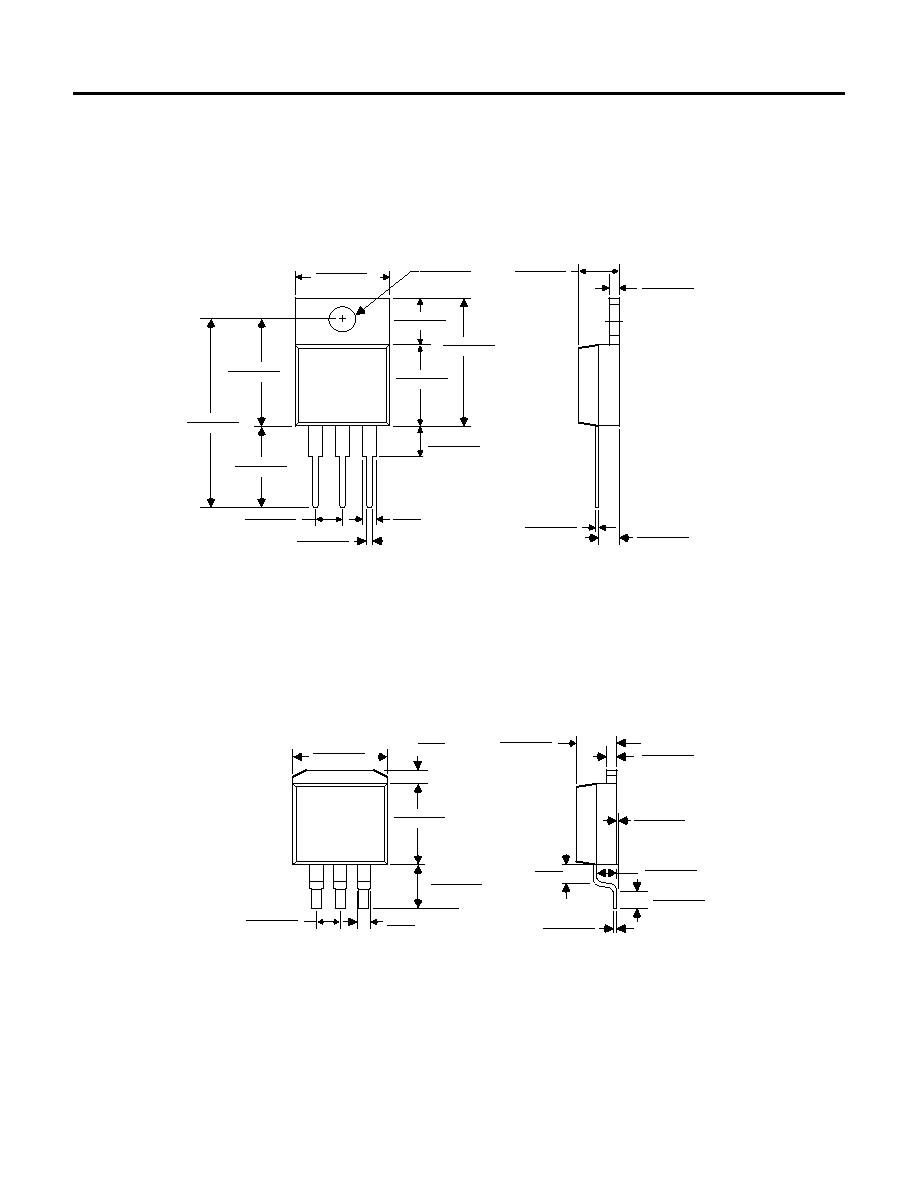
3 LEAD TO-220 PLASTIC PACKAGE (T)
3 LEAD TO-263 PLASTIC DD (M)
0.330-0.370
0.050
(8.382-9.398)
0.090-0.110
(2.286-2.794)
(1.270)
TYP
0.390-0.415
(9.906-10.541)
0.165-0.180
(4.191-4.572)
0.045-0.055
(1.143-1.397)
0.095-0.115
(2.413-2.921)
0.013-0.023
(0.330-0.584)
T (TO-220) AMS DRW# 042193
0.147-0.155
(3.734-3.937)
DIA
0.230-0.270
(5.842-6.858)
0.460-0.500
(11.684-12.700)
0.570-0.620
(14.478-15.748)
0.218-0.252
(5.537-6.401)
0.520-0.570
(13.208-14.478)
0.980-1.070
(24.892-27.178)
0.028-0.038
(0.711-0.965)
0.330-0.370
0.032
0.060
(1.524)
TYP
(8.382-9.398)
(5.05-5.54 )
0.090-0.110
(2.286-2.794)
0.199-0.218
(0.81)
TYP
0.390-0.415
(9.906-10.541)
0.165-0.180
(4.191-4.572)
0.045-0.055
(1.143-1.397)
0.095-0.115
(2.413-2.921)
0.90-0.110
(2.29-2.79)
0.013-0.023
(0.330-0.584)
0.108
(2.74)
TYP
(
0.102
)
+0.203
-0.102
0.004 +0.008
-0.004
M (DD3) AMS DRW# 042191R1
Advanced Monolithic Systems, Inc. 6680B Sierra Lane, Dublin, CA 94568 Phone (925) 556-9090 Fax (925) 556-9140
AMS2954
PACKAGE DIMENSIONS
inches (millimeters) unless otherwise noted (Continued).
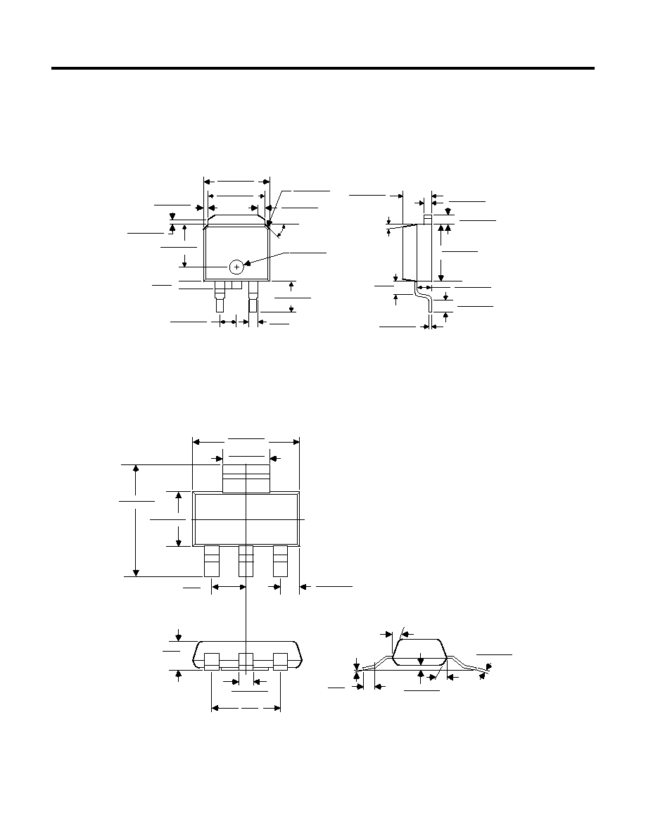
TO-252 PLASTIC PACKAGE (D)
3 LEAD SOT-223 PLASTIC PACKAGE
0.030
(0.762)
TYP
0.085-0.095
(2.159-2.413)
0.030-0.034
(0.762-0.863)
0.024±0.002
(0.610±0.0508)
0.018-0.022
(0.451-0.558)
0.038
(0.965)
TYP
D (D3) AMS DRW# 042891
0.038-0.042
(0.965-1.066)
0.038-0.042
(0.965-1.066)
0.235-0.245
(5.969-6.223)
0.088-0.092
(2.235-2.336)
0.099-0.103
(2.514-2.615)
0.175-0.180
(4.191-4.445)
0.023-0.027
(0.584-0.685)
0.020-0.030
(0.508-0.762)
0.258-0.262
(6.553-6.654)
0.033-0.037
(0.838-0.939)
0.020-0.030
(0.508-0.762)
0.208-0.212
(5.283-5.384)
0.025
(0.635)
TYP
0.057-0.067
(0.144-0.170)
DIA
45.0∞
7.0∞
0.130-0.146
(3.30-3.71)
0.248-0.264
(6.30-6.71)
0.116-0.124
(2.95-3.15)
0.264-0.287
(6.71-7.29)
0.090
(2.29)
NOM
0.071
(1.80)
MAX
0.033-0.041
(0.84-1.04)
0.025-0.033
(0.64-0.84)
0.181
(4.60)
NOM
0.012
(0.31)
MIN
0.025-0.033
(0.64-0.84)
10∞
MAX
10∞-16∞
10∞-16∞
0.010-0.014
(0.25-0.36)
(SOT-223 ) AMS DRW# 042292
Advanced Monolithic Systems, Inc. 6680B Sierra Lane, Dublin, CA 94568 Phone (925) 556-9090 Fax (925) 556-9140
AMS2954
PACKAGE DIMENSIONS
inches (millimeters) unless otherwise noted (Continued).
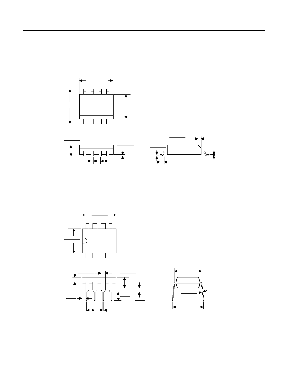
8 LEAD SOIC PLASTIC PACKAGE (S)
8 LEAD PLASTIC DIP PACKAGE (P)
0∞-8∞ TYP
0.010-0.020
(0.254-0.508)
S (SO-8 ) AMS DRW# 042293
x 45∞
0.016-0.050
(0.406-1.270)
0.008-0.010
(0.203-0.254)
0.004-0.010
(0.101-0.254)
0.014-0.019
(0.355-0.483)
0.053-0.069
(1.346-1.752)
0.050
(1.270)
TYP
0.150-0.157**
(3.810-3.988)
0.228-0.244
(5.791-6.197)
0.189-0.197*
(4.801-5.004)
*DIMENSION DOES NOT INCLUDE MOLD FLASH. MOLD FLASH
SHALL NOT EXCEED 0.006" (0.152mm) PER SIDE
**DIMENSION DOES NOT INCLUDE INTERLEAD FLASH. INTERLEAD
FLASH SHALL NOT EXCEED 0.010" (0.254mm) PER SIDE
1
2
3
4
8
7
6
5
0.045-0.065
(1.143-1.651)
0.255±0.015*
(6.477±0.381)
0.400*
(10.160)
MAX
1
2
3
4
8
7
6
5
0.130±0.005
(3.302±0.127)
0.018±0.003
(0.457±0.076)
0.100±0.010
(2.540±0.254)
(
8.255
)
+0.635
-0.381
0.325 +0.025
-0.015
0.009-0.015
(0.229-0.381)
0.300-0.325
(7.620-8.255)
0.065
(1.651)
TYP
0.005
(0.127)
MIN
0.125
(3.175)
MIN
0.015
(0.380)
MIN
*DIMENSIONS DO NOT INCLUDE MOLD FLASH OR PROTUSIONS.
MOLD FLASH OR PROTUSIONS SHALL NOT EXCEED 0.010" (0.254mm)
P (8L PDIP ) AMS DRW# 042294