Advanced Monolithic Systems, Inc. 6680B Sierra Lane, Dublin, CA 94568 Phone (925) 556-9090 Fax (925) 556-9140
Advanced
AMSOP-07
Monolithic
LOW OFFSET VOLTAGE OPERATIONAL AMPLIFIER
Systems
FEATURES
APPLICATIONS
∑
∑
Low V
OS
.............................................. 75
µ
µ
V Max
∑
∑
High-Gain Instrumentation
∑
∑
Low V
OS
Drift................................... 1.3
µ
µ
V/
∞
∞
C Max
∑
∑
Precision Data Acquisition
∑
∑
Ultra Stable with Time.................. 1.5
µ
µ
V/Month Max
∑
∑
Precision Integrators
∑
∑
Low Noise .........................................0.6
µ
µ
V
P-P
Max
∑
∑
Precision Threshold Detectors
∑
∑
Wide Input Voltage Range .............................
±
±
14V
∑
∑
Biomedical Amplifiers
∑
∑
Wide Supply Voltage Range ..................
±
±
3V to
±
±
18V
GENERAL DESCRIPTION
The AMSOP-07 is a precision operational amplifier with a very low input offset voltage. This device features a wide input
voltage range of
±
13V minimum, low input bias current, high impedance, high CMRR, excellent stability of offsets and gain
over time and temperature. Excellent linearity can be maintained even at high closed-loop gains.
Low cost, low noise, low offsets and high open-loop gain make the AMSOP-07 an excellent choice particularly for high-gain
instrumentation applications. Other applications include precision data acquisition, precision integrators, threshold detectors
and medical instrumentation.
The AMSOP-07 is operational in the full industrial temperature range of -40
∞
C to 85
∞
C and is available in the 8 lead SOIC
and plastic dip (PDIP) packages.
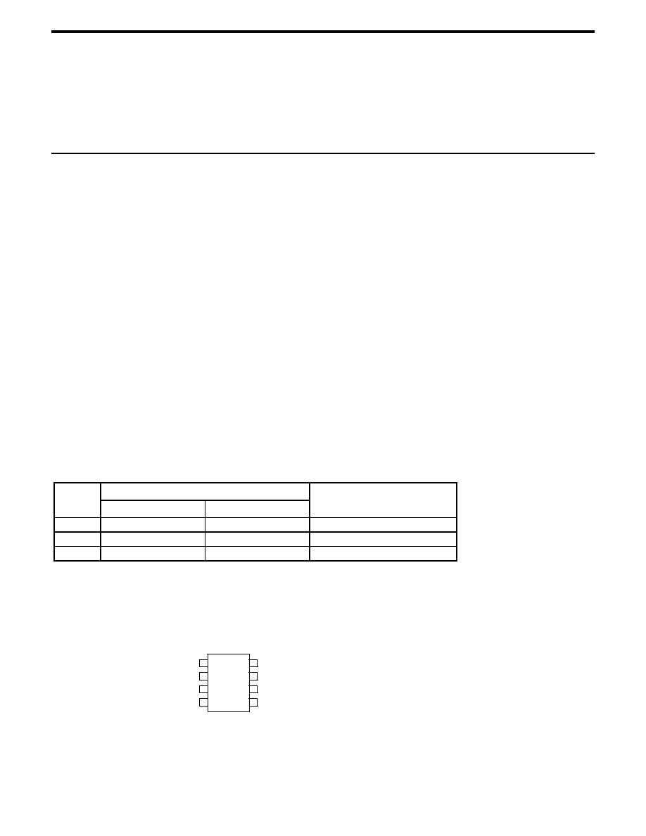
ORDERING INFORMATION
:
TOL.
PACKAGE TYPE
OPERATING
8 LEAD SOIC
8 LEAD PDIP
TEMPERATURE RANGE
±
75
µ
V AMSOP-07ES
AMSOP-07EP
-40 to 85
∞
C
±
150
µ
V AMSOP-07CS
AMSOP-07CP
-40 to 85
∞
C
±
150
µ
V AMSOP-07DS
AMSOP-07DP
-40 to 85
∞
C
PIN CONNECTIONS
8 Lead SOIC/ 8Lead PDIP
Top View
1
2
8
4
3
7
5
6
OUT
N/C
V+
V
OS
TRIM
-IN
+IN
V
OS
TRIM
V-
Advanced Monolithic Systems, Inc. 6680B Sierra Lane, Dublin, CA 94568 Phone (925) 556-9090 Fax (925) 556-9140
AMSOP-07
ABSOLUTE MAXIMUM RATINGS
(Note1)
Supply Voltage
±
22V
Storage temperature
-65
∞
C to +125
∞
C
Differential Input Voltage
±
30V
Junction Temperature
+150
∞
C
Input Voltage
±
22V
Soldering information (60 sec)
300
∞
C
Output Short Circuit Duration
Indefinite
Thermal Resistance
Operating Temperature Range
-40
∞
C to 85
∞
C
8 L SOIC
158
∞
C/W
8 L PDIP
103
∞
C/W
ELECTRICAL CHARACTERISTICS
Electrical Characteristics at V
IN
=
±
15V and T
A
= +25∞C unless otherwise specified.
Parameter
Conditions
AMSOP-07E
AMSOP-07 C
AMSOP-07 D
Units
Min
Typ
Max
Min
Typ
Max
Min
Typ
Max
Input Offset Voltage
(Note 2)
30
75
60
150
60
150
µ
V
Long Term V
OS
Stability
(Note 3)
0.3
1.5
0.4
2.0
0.5
3.0
µ
V/Mo
Input Offset Current
0.5
3.8
0.8
6.0
0.8
6.0
nA
Input Bias Current
±
1.2
±
4.0
±
1.8
±
7.0
±
2.0
±
12
nA
Input Noise Voltage
0.1Hz to 10Hz
0.35
0.6
0.38
0.65
0.38
0.65
µ
V
P-P
Input Noise Voltage
Density
f
O
= 10Hz
f
O
= 100Hz (Note 4)
f
O
= 1000Hz
10.3
10.0
9.6
18.0
13.0
11.0
10.5
10.2
9.8
20.0
13.5
11.5
10.5
10.3
9.8
20.0
13.5
11.5
nV/
Hz
Input Noise Current
0.1Hz to 10Hz
14
30
15
35
15
35
pA
P-P
Input Noise
CurrentDensity
f
O
= 10Hz
f
O
= 100Hz (Note 4)
f
O
= 1000Hz
0.32
0.14
0.12
0.80
0.23
0.17
0.35
0.15
0.13
0.90
0.27
0.18
0.35
0.15
0.13
0.90
0.27
0.18
pA/
Hz
Input Resistance
Differential-Mode
(Note 5)
15
50
8
33
7
31
M
Input Resistance
Common-Mode
160
120
120
G
Input Voltage Range
±
13
±
14
±
13
±
14
±
13
±
14
V
Common-Mode
Rejection Ratio
V
CM
=
±
13
106
123
100
120
94
110
dB
Power Supply
Rejection Ratio
V
S
=
±
13 to
±
18
5
20
7
32
7
32
µ
V/V
Large-Signal
Voltage Gain
R
L
2k
, V
O
=
±
10V
R
L
500
, V
O
=
±
0.5V,
V
S
=
±
0.5V (Note 5)
200
150
500
400
120
100
400
400
120
400
400
V/mV
Output Voltage
Swing
R
L
10k
R
L
2k
R
L
1k
±
12.5
±
12.0
±
10.5
±
13.0
±
12.8
±
12.0
±
12.0
±
11.5
±
13.0
±
12.8
±
12.0
±
12.0
±
11.5
±
13.0
±
12.8
±
12.0
V
Slew Rate
R
L
2k
(Note 4)
0.1
0.3
0.1
0.3
0.1
0.3
V/
µ
s
Closed-Loop
Bandwidth
A
VCL
=+1
(Note 6)
0.4
0.6
0.4
0.6
0.4
0.6
MHz
Open-Loop Output
Resistance
V
O
= 0, I
O
= 0
60
60
60
Power Consumption
V
S
=
±
15V, No Load
V
S
=
±
3V, No Load
75
4
120
6
80
4
150
8
80
4
150
8
mW
Offset Adjustment
Range
R
P
=20k
±
4
±
4
±
4
mV

Advanced Monolithic Systems, Inc. 6680B Sierra Lane, Dublin, CA 94568 Phone (925) 556-9090 Fax (925) 556-9140
AMSOP-07
ELECTRICAL CHARACTERISTICS
Electrical Characteristics at V
IN
=
±
15, at -40∞C
T
A
+85∞C unless otherwise specified.
Parameter
Conditions
AMSOP-07E
AMSOP-07 C
AMSOP-07 D
Units
Min
Typ
Max
Min
Typ
Max
Min
Typ
Max
Input Offset Voltage
(Note 2)
45
130
85
250
85
250
µ
V
Average Input Offset
Without External Trim
0.3
1.3
0.5
1.8
0.7
2.5
µ
V/
∞
C
Voltage Drift
(Note 5)
With External Trim
R
P
=2k
0.3
1.3
0.4
1.6
0.7
2.5
µ
V/
∞
C
Input Offset Current
0.9
5.3
1.6
8.0
1.6
8.0
nA
Average Input Offset
Current Drift
(Note 4)
8
35
12
50
12
50
pA/
∞
C
Input Bias Current
±
1.5
±
5.5
±
2.2
±
9.0
±
3.0
±
14
nA
Average Input Bias
Current Drift
(Note 4)
13
35
18
50
18
50
pA/
∞
C
Input Voltage Range
±
13
±
13.5
±
13
±
13.5
±
13
±
13.5
V
Common-Mode
Rejection Ratio
V
CM
=
±
13
103
123
97
120
94
106
dB
Power Supply
Rejection Ratio
V
S
=
±
13 to
±
18
7
32
10
51
10
51
µ
V/V
Large-Signal
Voltage Gain
R
L
2k
, V
O
=
±
10V
180
450
100
400
100
400
V/mV
Output Voltage
Swing
R
L
2k
±
12.0
±
13.0
±
12.0
±
13.0
±
12.0
±
13.0
V
Note 1:
Absolute Maximum Ratings indicate limits beyond which damage to the device may occur. Operating Ratings indicate conditions for which the device is
intended to be functional, but do not guarantee specific performance limits. For guaranteed specifications and test conditions, see the Electrical Characteristics
.
The
guaranteed specifications apply only for the test conditions listed.
Note 2:
Input Offset Voltage measurements are performed by automated test equipment approximately 0.5 seconds after application of power.
Note 3:
Long-Term Input Offset Voltage Stability refers to the averaged trend line of VOS vs. Time over extended periods after the first 30 days of operation.
Excluding the initial hour of operation, changes in VOS during the first 30 operating days are typically 2.5
µ
V. Parameter is sample tested.
Note 4:
Sample tested
Note 5:
Guaranteed by design.
Note 6:
Guaranteed but not tested.
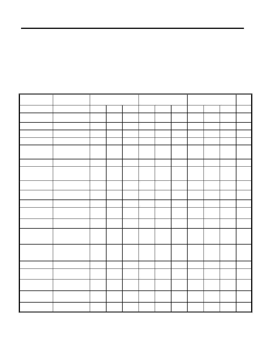
TYPICAL PERFORMANCE CHARACTERISTICS
Input Bias Current vs
Differrential Input Voltage
DIFFERENTIAL INPUT VALUE (V)
NONINVERTING INPUT BIAS
CURRENT (mA)
V
S
= ±15V
-30
-20
-10
0
10
20
30
AT | V
DIFF
|
1.0V, | IB |
7nA (OP-07C)
0
50
1000
400
100
OPEN-LOOP GAIN (V/mV)
Open-Loop Gain vs Temperature
TEMPERATURE (∞ C)
600
200
-50
0
-30
-20
-10
0
10
20
30
-30
-20
-10
0
10
20
30
INVERTING INPUT BIAS
800
2
3
25
10
5
ABSOLUTE CHANGE IN INPUT
OFFSET VOLTAGE (
µ
V)
Warm-UpDrift
TIME AFTER POWER SUPPLY TURN-ON (minutes)
15
5
1
0
20
V
S
= ±15V
V
S
= ±15V
0
4
OP-07C
OP-07E
T
A
= 25∞ C
T
A
= 25∞ C

Advanced Monolithic Systems, Inc. 6680B Sierra Lane, Dublin, CA 94568 Phone (925) 556-9090 Fax (925) 556-9140
AMSOP-07
TYPICAL PERFORMANCE CHARACTERISTICS (Continued)
0
1
4
-50
0
50
100
TEMPERATURE (∞ C)
Input Bias Current vs Temperature
INPUT BIAS CURRENT (
nA)
2
3
OP-07C
FREQUENCY (Hz)
PEAK-TO-PEAK AMPLITUEDE (V)
0
28
Maximum Output Swing vs
Frequency
16
12
4
100k
1M
1k
10k
8
24
20
0
±10
±15
1000
400
±20
OPEN-LOOP GAIN (V/mV)
Open-Loop Gain vs Power
Supply Voltage
POWER SUPPLY VOLTAGE (V)
600
200
±5
0
0
0.5
1.5
1.0
2.5
-50
0
50
100
TEMPERATURE (∞ C)
Input Offset Current vs Temperature
INPUT OFFSET CURRENT (
nA)
2.0
OP-07E
-40
0
120
0
1
10 100 1k 10k 100k 1M 10M
FREQUENCY (Hz)
Open-Loop Frequency Response
OPEN-LOOP GAIN (dB)
40
80
0
5
20
100
1k
10k
LOAD RESISTANCE TO GROUND (
)
Maximum Output Voltage vs
Load Resistance
MAXIMUM OUTPUT VOLTAGE (V)
10
15
800
0
50
85
100
ABSOLUTE VALUE OF OFFSET
VOLTAGE (
µ
V)
Untrimmed Offset Voltage vs
Temperature
TEMPERATURE (∞ C)
50
25
-50
0
75
15
20
35
0
1
2
3
4
TIME FROM OUTPUT BEING SHORTED (minutes)
Output Short-Circuit Current vs
Time
OUTPUT SHORT-CIRCUIT
CURRENT (mA)
25
30
1. V
IN
(PIN 3) = -10mV, V
O
= +15V
V
S
= ±15V
V
S
= ±15V
T
A
= 25∞ C
V
S
= ±15V
T
A
= 25∞ C
V
S
= ±15V
T
A
= 25∞ C
V
S
= ±15V
T
A
= 25∞ C
V
S
= ±15V
T
A
= 25∞ C
V
S
= ±15V
R
S
= 100
V
IN
= ±10mV
OP-07E
OP-07C
POSITIVE SWING
NEGATIVE SWING
OP-07C
OP-07E
2. V
IN
(PIN 3) = +10mV, V
O
= -15V
1
1
2
2
Advanced Monolithic Systems, Inc. 6680B Sierra Lane, Dublin, CA 94568 Phone (925) 556-9090 Fax (925) 556-9140
AMSOP-07
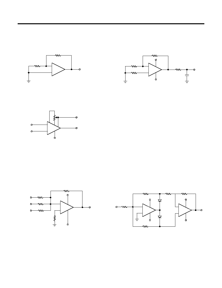
TEST CIRCUITS
TYPICAL OFFSET VOLTAGE TEST CIRCUIT
TYPICAL LOW-FREQUENCY NOISE TEST CIRCUIT
OPTIONAL OFFSET NULLING CIRCUIT
TYPICAL APPLICATIONS
Adjustment Free Precision Summing Amplifier
Precision Absolute Value Circuit
OP-07
A1
+
-
R3
10k
FD333
D1
V-
V+
4
6
7
2
3
R4
10k
FD333
D1
R5
10k
OP-07
A2
+
-
V-
4
7
2
3
6
V
A
R2
10k
R1
10k
V+
E
O
0 TO +10V
E
IN
±10V
OP-07
+
-
R4
10k
R2
10k
E
O
V-
V+
R1
10k
4
6
7
2
3
R3
10k
E
1
E
2
E
3
R5
2.5k
OP-07
+
-
V-
4
6
7
2
3
1
8
V+
OUTPUT
-
+
INPUT
20k
OP-07
+
-
200k
50k
V
O
V
OS
= V
O
/4000
OP-07
+
-
2.5M
100k
OUTPUT
4.7
µ
F
V-
V+
100k
3.3k
(
10Hz FILTER)
4
6
7
2
3
INPUT REFERRED NOISE = VO/25,000 =(5mV/cm)/25,000 = 200nV/cm