Advanced Monolithic Systems, Inc. 6680B Sierra Lane, Dublin, CA 94568 Phone (925) 556-9090 Fax (925) 556-9140
Advanced
AMSREF-01
Monolithic
+10V PRECISION VOLTAGE REFERENCE
Systems
FEATURES
APPLICATIONS
∑
∑
10 Volt Output ...................................
±
±
0.3% Max
∑
∑
A/D, D/A Converters
∑
∑
Adjustment Range .................................
±
±
3% Min
∑
∑
Portable Instrumentation
∑
∑
Excellent Temperature Stability............... 8.5ppm/
∞
∞
C
∑
∑
Digital Voltmeters
∑
∑
Low Noise ......................................... 30
µ
µ
V
P-P
Max
∑
∑
Current sources
∑
∑
Low Supply Current ............................ 650
µ
µ
A Typ
∑
∑
Wide Input Voltage Range ...................... 12V to 40V
∑
∑
High Load-Driving Capability......................... 20mA
∑
∑
No External Components
∑
∑
Short -Circuit Proof
GENERAL DESCRIPTION
The AMSREF-01 is a precision voltage reference, which provides a stable +10V output, which can be adjusted over a
±
3%
range with minimal effect on temperature stability. Careful design of this device improved its bandgap and as a result
excellent temperature stability is achieved. The operating supply range is 12V to 40V with a typical current drain of 650
µ
A.
Low cost, low noise and low power makes the AMSREF-01 an excellent choice whenever a stable voltage reference is
required. Applications include D/A and A/D converters, portable instrumentation and digital voltmeters.
The AMSREF-01 is operational in the full industrial temperature range of -40
∞
C to +85
∞
C and is available in the 8 lead
SOIC and plastic dip (PDIP) packages.
ORDERING INFORMATION
:
TOL.
PACKAGE TYPE
OPERATING
8 LEAD SOIC
8 LEAD PDIP
TEMPERATURE RANGE
±
30mV AMSREF-01ES
AMSREF-01EP
-40 to 85
∞
C
±
50mV AMSREF-01HS
AMSREF-01HP
-40 to 85
∞
C
±
100mV AMSREF-01CS
AMSREF-01CP
-40 to 85
∞
C
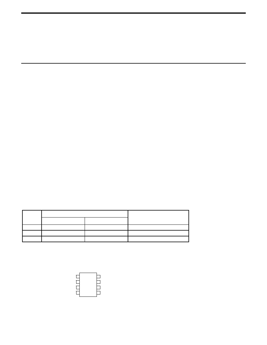
PIN CONNECTIONS
8L SOIC/ 8L PDIP
Top View
1
2
8
4
3
7
5
6 V
OUT
TRIM
N/C
N/C
V
IN
N/C
N/C
GND

Advanced Monolithic Systems, Inc. 6680B Sierra Lane, Dublin, CA 94568 Phone (925) 556-9090 Fax (925) 556-9140
AMSREF-01
ABSOLUTE MAXIMUM RATINGS
(Note1)
Input Voltage
40V
Storage temperature
-65
∞
C to +125
∞
C
Output Short Circuit Duration
Soldering information (60 sec)
300
∞
C
(to Ground or V
IN
)
Indefinite
Thermal Resistance
Operating Temperature Range
-40
∞
C to 85
∞
C
8 L SOIC
160
∞
C/W
Junction Temperature
-65
∞
C to +150
∞
C
8 L PDIP
110
∞
C/W
ELECTRICAL CHARACTERISTICS
Electrical Characteristics at V
IN
=+15V and T
A
= +25∞C unless otherwise specified.
Parameter
Conditions
AMSREF-01E
AMSREF-01 H
AMSREF-01 C
Units
Min
Typ
Max
Min
Typ
Max
Min
Typ
Max
Output Voltage
I
L
= 0
9.97
10.0
10.03
9.95
10.0
10.05
9.90
10.0
10.10
V
Output Adjustment
Range
R
P
=10k
±
3.0
±
3.3
±
3.0
±
3.3
±
2.7
±
3.3
%
Output Voltage Noise
0.1Hz to 10Hz
20
30
20
30
25
35
µ
V
P-P
Line Regulation
(Note 5)
V
IN
= 13V to 33V
0.006
0.010
0.006
0.010
0.009
0.015
% V
Load Regulation
(Note 5)
I
L
= 0 to 10 mA,
0.005
0.008
0.006
0.010
0.006
0.015
% mA
Turn-on Setting Time
T
O
±
0.1% of final
value
5
5
5
µ
s
Quiescent Supply
Current
No Load
0.65
1.0
0.65
1.0
0.65
1.0
mA
Load Current
10
21
10
21
8
21
mA
Sink Current
(Note 6)
-5
-10
-5
-10
-5
-10
mA
Short Circuit Current
V
O
= 0
30
30
30
mA
ELECTRICAL CHARACTERISTICS
Electrical Characteristics at V
IN
= 15, I
L
= 0mA, and -40∞C
T
A
+85∞C unless otherwise specified.
Parameter
Conditions
AMSREF-01E
AMSREF-01 H
AMSREF-01 C
Units
Min
Typ
Max
Min
Typ
Max
Min
Typ
Max
Output Voltage
Change with Temp.
(Notes 2,3)
0.02
0.06
0.07
0.17
0.14
0.45
%
Output Voltage Temp.
Coefficient
(Note 4)
3
8.5
10
25
20
65
ppm/∞C
Change in V
O
Temp.
Coefficient with
Output Adjustment
R
L
= 10k
0.7
0.7
0.7
ppm/∞C
Line Regulation
(Note 5)
V
IN
= 13V to 33V
0.007
0.012
0.007
0.012
0.011
0.018
% V
Load Regulation
(Note 5)
I
L
= 0 to 8 mA,
0.006
0.010
0.007
0.012
0.008
0.018
% mA
Note 1:
Absolute Maximum Ratings indicate limits beyond which damage to the device may occur. Operating Ratings indicate conditions for which the device is
intended to be functional, but do not guarantee specific performance limits. For guaranteed specifications and test conditions, see the Electrical Characteristics
.
The
guaranteed specifications apply only for the test conditions listed.

Advanced Monolithic Systems, Inc. 6680B Sierra Lane, Dublin, CA 94568 Phone (925) 556-9090 Fax (925) 556-9140
AMSREF-01
Note 2:
The output voltage change with temperature (
V
OT
) is defined as the absolute difference between the maximum output voltage and the minimum output
voltage over the specified temperature range expressed as a percentage of 10V:
V
OT
=
[
(V
MAX
-V
MIN
)/10V
]
x 100
Note 3:
V
OT
specification applies trimmed to +10.000V or untrimmed
Note 4:
TCV
O
is defined as
V
OT
divided by the temperature range: TCV
O
(-40
∞
C to +85
∞
C)=
[
V
OT
(-40
∞
C to +85
∞
C)
]
/ 125
∞
C
Note 5:
Line and Load Regulation specifications include the effect of self heating.
Note 6:
During sink current test, the device meets the output voltage specified.
TYPICAL PERFORMANCE CHARACTERISTICS
Normalized Load Regulation (
I
L
= 10mA)
vs Temperature
TEMPERATURE (∞ C)
-60 -40
20
60
100
0.6
1.1
1.3
1.4
1.2
1.0
0.9
0.8
0.7
LOAD REG (T)/ LOAD REG (25∞ C)
V
IN
= 15V
-20 0
40
80
120 140
0
5
35
0
15
20
30
INPUT VOLTAGE (V)
Maximum Load Current vs
Input Voltage
MAXIMUM LOAD CURRENT (mA)
20
25
25
10
15
30
Normalized Line Regulation (
I
L
= 10mA vs
Temperature
TEMPERATURE (∞ C)
-60 -40
20
60
100
0.6
1.1
1.3
1.4
1.2
1.0
0.9
0.8
0.7
LINE REG (T)/ LINE REG (25∞ C)
-20 0
40
80
120 140
Maximum Load Current vs
Temperature
TEMPERATURE (∞ C)
-60 -40
20
60
100
0
20
25
30
15
10
5
MAXIMUM LOAD CURRENT (mA)
V
IN
= 15V
-20 0
40
80
120 140
QUIESCENT CURRENT (mA)
TEMPERATURE (∞ C)
-60 -40
20
60
100
0.7
1.1
1.2
1.3
1.0
0.9
0.8
V
IN
= 15V
-20 0
40
80
120 140
Quiescent Current vs
Temperature
SHORT CIRCUIT PROTECTION
500mW MAXIMUM
DISSIPATION
T
A
= 25∞ C

Advanced Monolithic Systems, Inc. 6680B Sierra Lane, Dublin, CA 94568 Phone (925) 556-9090 Fax (925) 556-9140
AMSREF-01
OUTPUT ADJUSTMENT
The REF-01 trim terminal can be used to adjust the 10V output
voltage
±
300mV. This feature allows the system designer to trim
system errors by setting the reference to a voltage other than 10V.
The system can also be set exactly 10.000V, or to 10.240V for
binary applications.
Adjustment of the output does not significantly affect the
temperature performance of the device. The temperature coefficient
change is approximately 0.7ppm/
∞
C for 100mV of output
adjustment.
GND
TRIM
10k
OUTPUT
V
IN
V
O
+15V
2
6
5
4
REF-01
TYPICAL APPLICATIONS
±
±
10V Reference
Precision Calibration Standard
Supply Bypassing
For best results, it is recommended that the power supply pin is bypassed with a
0.1
µ
F disk ceramic capacitor.
Current Source
Current Sink
GND
TRIM
10k
V
IN
V
O
+15V
2
6
5
4
REF-01
+15V
-15V
10k
5k
-10V
+10V
0.1
µ
F
OP-02
-
+
GND
TRIM
100k
V
IN
V
O
9V
2
6
5
4
REF-01
9V
10.000V
+
-
0.1
µ
F
1.1mA
GND
TRIM
R
V
IN
V
O
-15V
2
6
5
4
REF-01
I
OUT
I
OUT
=
(10.0V/R)+1mA
VOLTAGE COMPLIANCE: -3V TO +25V
GND
TRIM
R
V
IN
V
O
+15V
2
6
5
4
REF-01
I
OUT
I
OUT
=
(10.0V/R)+1mA
VOLTAGE COMPLIANCE: -25V TO +3V
Advanced Monolithic Systems, Inc. 6680B Sierra Lane, Dublin, CA 94568 Phone (925) 556-9090 Fax (925) 556-9140
AMSREF-01
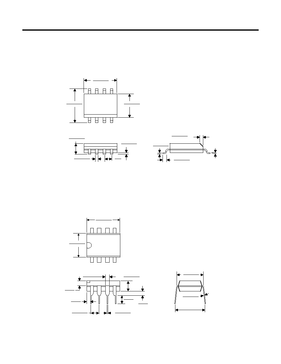
PACKAGE DIMENSIONS inches (millimeters) unless otherwise noted.
8 LEAD SOIC PLASTIC PACKAGE (S)
8 LEAD PLASTIC DIP PACKAGE (P)
0∞-8∞ TYP
0.010-0.020
(0.254-0.508)
S (SO-8 ) AMS DRW# 042293
x 45∞
0.016-0.050
(0.406-1.270)
0.008-0.010
(0.203-0.254)
0.004-0.010
(0.101-0.254)
0.014-0.019
(0.355-0.483)
0.053-0.069
(1.346-1.752)
0.050
(1.270)
TYP
0.150-0.157**
(3.810-3.988)
0.228-0.244
(5.791-6.197)
0.189-0.197*
(4.801-5.004)
*DIMENSION DOES NOT INCLUDE MOLD FLASH. MOLD FLASH
SHALL NOT EXCEED 0.006" (0.152mm) PER SIDE
**DIMENSION DOES NOT INCLUDE INTERLEAD FLASH. INTERLEAD
FLASH SHALL NOT EXCEED 0.010" (0.254mm) PER SIDE
1
2
3
4
8
7
6
5
0.045-0.065
(1.143-1.651)
0.255±0.015*
(6.477±0.381)
0.400*
(10.160)
MAX
1
2
3
4
8
7
6
5
0.130±0.005
(3.302±0.127)
0.018±0.003
(0.457±0.076)
0.100±0.010
(2.540±0.254)
(
8.255
)
+0.635
-0.381
0.325 +0.025
-0.015
0.009-0.015
(0.229-0.381)
0.300-0.325
(7.620-8.255)
0.065
(1.651)
TYP
0.005
(0.127)
MIN
0.125
(3.175)
MIN
0.015
(0.380)
MIN
*DIMENSIONS DO NOT INCLUDE MOLD FLASH OR PROTUSIONS.
MOLD FLASH OR PROTUSIONS SHALL NOT EXCEED 0.010" (0.254mm)
P (8L PDIP ) AMS DRW# 042294