050-7187 Rev A 11-2003
MAXIMUM RATINGS
All Ratings: T
C
= 25∞C unless otherwise specified.
CAUTION: These Devices are Sensitive to Electrostatic Discharge. Proper Handling Procedures Should Be Followed.
APT Website - http://www.advancedpower.com
G
D
S
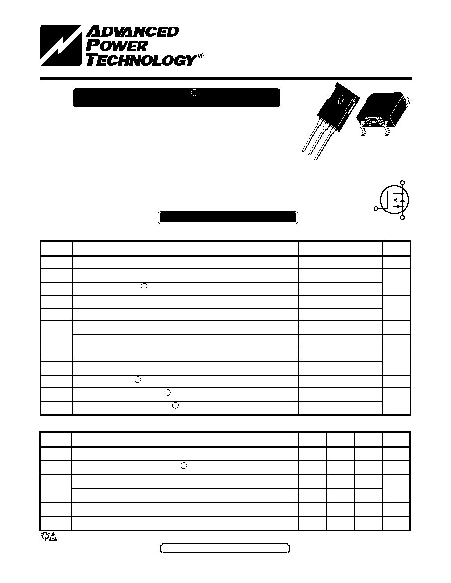
Power MOS 7
Æ
is a new generation of low loss, high voltage, N-Channel
enhancement mode power MOSFETS. Both conduction and switching
losses are addressed with Power MOS 7
Æ
by significantly lowering R
DS(ON)
and Q
g
. Power MOS 7
Æ
combines lower conduction and switching losses
along with exceptionally fast switching speeds inherent with APT's
patented metal gate structure.
POWER MOS 7
R
FREDFET
∑ Lower Input Capacitance
∑ Increased Power Dissipation
∑ Lower Miller Capacitance
∑ Easier To Drive
∑ Lower Gate Charge, Qg
∑ TO-247 or Surface Mount D
3
PAK Package
∑
FAST RECOVERY BODY DIODE
Characteristic / Test Conditions
Drain-Source Breakdown Voltage (V
GS
= 0V, I
D
= 250µA)
Drain-Source On-State Resistance
2
(V
GS
= 10V, 6.5A)
Zero Gate Voltage Drain Current (V
DS
= 1100V, V
GS
= 0V)
Zero Gate Voltage Drain Current (V
DS
= 880V, V
GS
= 0V, T
C
= 125∞C)
Gate-Source Leakage Current (V
GS
= ±30V, V
DS
= 0V)
Gate Threshold Voltage (V
DS
= V
GS
, I
D
= 1mA)
Symbol
V
DSS
I
D
I
DM
V
GS
V
GSM
P
D
T
J
,T
STG
T
L
I
AR
E
AR
E
AS
Parameter
Drain-Source Voltage
Continuous Drain Current @ T
C
= 25∞C
Pulsed Drain Current
1
Gate-Source Voltage Continuous
Gate-Source Voltage Transient
Total Power Dissipation @ T
C
= 25∞C
Linear Derating Factor
Operating and Storage Junction Temperature Range
Lead Temperature: 0.063" from Case for 10 Sec.
Avalanche Current
1
(Repetitive and Non-Repetitive)
Repetitive Avalanche Energy
1
Single Pulse Avalanche Energy
4
UNIT
Volts
Amps
Volts
Watts
W/∞C
∞C
Amps
mJ
STATIC ELECTRICAL CHARACTERISTICS
Symbol
BV
DSS
R
DS(on)
I
DSS
I
GSS
V
GS(th)
UNIT
Volts
Ohms
µA
nA
Volts
MIN
TYP
MAX
1100
1.00
100
500
±100
3
5
APT1101RBFLL_SFLL
1100
13
52
±30
±40
403
3.23
-55 to 150
300
13
30
1300
TO-247
D
3
PAK
APT1101RBFLL
APT1101RSFLL
1100V 13A 1.000
DYNAMIC CHARACTERISTICS
050-7187 Rev A 11-2003
APT1101RBFLL_SFLL
SOURCE-DRAIN DIODE RATINGS AND CHARACTERISTICS
THERMAL CHARACTERISTICS
Characteristic / Test Conditions
Continuous Source Current (Body Diode)
Pulsed Source Current
1
(Body Diode)
Diode Forward Voltage
2
(V
GS
= 0V, I
S
= -13A)
Peak Diode Recovery
dv
/
dt
5
Reverse Recovery Time
(I
S
= -13A,
di
/
dt
= 100A/µs)
Reverse Recovery Charge
(I
S
= -13A,
di
/
dt
= 100A/µs)
Peak Recovery Current
(I
S
= -13A,
di
/
dt
= 100A/µs)
Symbol
I
S
I
SM
V
SD
dv
/
dt
t
rr
Q
rr
I
RRM
UNIT
Amps
Volts
V/ns
ns
µC
Amps
MIN
TYP
MAX
13
52
1.3
18
T
j
= 25∞C
210
T
j
= 125∞C
710
T
j
= 25∞C
1.0
T
j
= 125∞C
3.6
T
j
= 25∞C
10
T
j
= 125∞C
14
Symbol
R
JC
R
JA
MIN
TYP
MAX
0.31
40
UNIT
∞C/W
Characteristic
Junction to Case
Junction to Ambient
1 Repetitive Rating: Pulse width limited by maximum junction
temperature
2 Pulse Test: Pulse width < 380 µs, Duty Cycle < 2%
3 See MIL-STD-750 Method 3471
4 Starting T
j
=
+25∞C, L = 15.38mH, R
G
=
25
, Peak I
L
= 13A
5
dv
/
dt
numbers reflect the limitations of the test circuit rather than the
device itself.
I
S
-
13A
di
/
dt
700A/µs
V
R
1100
T
J
150
∞
C
6 Eon includes diode reverse recovery. See figures 18, 20.
APT Reserves the right to change, without notice, the specifications and information contained herein.
Symbol
C
iss
C
oss
C
rss
Q
g
Q
gs
Q
gd
t
d(on)
t
r
t
d(off)
t
f
E
on
E
off
E
on
E
off
Characteristic
Input Capacitance
Output Capacitance
Reverse Transfer Capacitance
Total Gate Charge
3
Gate-Source Charge
Gate-Drain ("Miller") Charge
Turn-on Delay Time
Rise Time
Turn-off Delay Time
Fall Time
Turn-on Switching Energy
6
Turn-off Switching Energy
Turn-on Switching Energy
6
Turn-off Switching Energy
MIN
TYP
MAX
2345
388
65
90
12
61
12
7
32
14
364
105
748
139
UNIT
pF
nC
ns
µ
J
Test Conditions
V
GS
= 0V
V
DS
= 25V
f
= 1 MHz
V
GS
= 10V
V
DD
= 550V
I
D
= 13A
@ 25∞C
RESISTIVE SWITCHING
V
GS
=
15V
V
DD
=
550V
I
D
=
13A
@ 25∞C
R
G
=
1.6
INDUCTIVE SWITCHING @ 25∞C
V
DD
=
733V, V
GS
= 15V
I
D
=
13A, R
G
=
5
INDUCTIVE SWITCHING @ 125∞C
V
DD
=
733V, V
GS
= 15V
I
D
=
13A, R
G
=
5
Note:
Duty Factor D = t1/t2
Peak TJ = PDM x Z
JC + TC
t1
t2
P
DM
SINGLE PULSE
Z
JC
, THERMAL IMPEDANCE (∞C/W)
10
-5
10
-4
10
-3
10
-2
10
-1
1.0
RECTANGULAR PULSE DURATION (SECONDS)
FIGURE 1, MAXIMUM EFFECTIVE TRANSIENT THERMAL IMPEDANCE, JUNCTION-TO-CASE vs PULSE DURATION
0.35
0.30
0.25
0.20
0.15
0.10
0.05
0
0.5
0.1
0.3
0.7
0.9
0.05
050-7187 Rev A 11-2003
Typical Performance Curves
APT1101RBFLL_SFLL
R
DS
(ON), DRAIN-TO-SOURCE ON RESISTANCE
I
D
, DRAIN CURRENT (AMPERES)
I
D
, DRAIN CURRENT (AMPERES)
(NORMALIZED)
V
GS
(TH), THRESHOLD VOLTAGE
BV
DSS
, DRAIN-TO-SOURCE BREAKDOWN
R
DS
(ON), DRAIN-TO-SOURCE ON RESISTANCE
I
D
, DRAIN CURRENT (AMPERES)
(NORMALIZED)
VOLTAGE (NORMALIZED)
5.5V
6V
6.5V
5V
VGS =15 & 10V
VGS=10V
VGS=20V
TJ = +125∞C
TJ = +25∞C
TJ = -55∞C
VDS> ID (ON) x RDS (ON)MAX.
250µSEC. PULSE TEST
@ <0.5 % DUTY CYCLE
V
DS
, DRAIN-TO-SOURCE VOLTAGE (VOLTS)
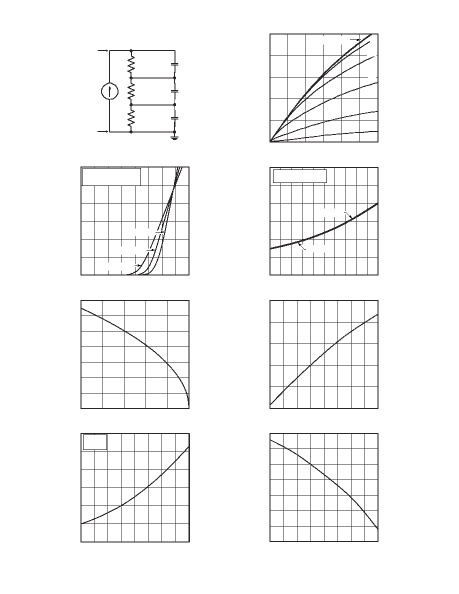
FIGURE 2, TRANSIENT THERMAL IMPEDANCE MODEL
FIGURE 3, LOW VOLTAGE OUTPUT CHARACTERISTICS
V
GS
, GATE-TO-SOURCE VOLTAGE (VOLTS)
I
D
, DRAIN CURRENT (AMPERES)
FIGURE 4, TRANSFER CHARACTERISTICS
FIGURE 5, R
DS
(ON) vs DRAIN CURRENT
T
C
, CASE TEMPERATURE (∞C)
T
J
, JUNCTION TEMPERATURE (∞C)
FIGURE 6, MAXIMUM DRAIN CURRENT vs CASE TEMPERATURE
FIGURE 7, BREAKDOWN VOLTAGE vs TEMPERATURE
T
J
, JUNCTION TEMPERATURE (∞C)
T
C
, CASE TEMPERATURE (∞C)
FIGURE 8, ON-RESISTANCE vs. TEMPERATURE
FIGURE 9, THRESHOLD VOLTAGE vs TEMPERATURE
7V
0
5
10
15
20
25
30
0
1
2
3
4
5
6
7
8
0
2
4
6
8
10 12 14 16 18 20
25
50
75
100
125
150
-50 -25
0
25
50
75
100 125 150
-50
-25
0
25
50
75
100 125 150
-50
-25
0
25
50
75 100 125 150
30
25
20
15
10
5
0
14
12
10
8
6
4
2
0
3
2.5
2.0
1.5
1.0
0.5
0
I
D = 6.5A
V
GS = 10V
NORMALIZED TO
V
GS
= 10V @ 6.5A
25
20
15
10
5
0
1.40
1.30
1.20
1.10
1.00
0.90
0.80
1.15
1.10
1.05
1.00
0.95
0.90
1.2
1.1
1.0
0.9
0.8
0.7
0.6
0.5
0.0258
0.107
0.177
0.00295F
0.0114F
0.174F
Power
(watts)
Junction
temp. (
∞
C)
RC MODEL
Case temperature. (
∞
C)
050-7187 Rev A 11-2003
APT1101RBFLL_SFLL
VDS= 550V
VDS= 220V
VDS= 880V
I
D = 6.5A
Crss
Ciss
Coss
V
DS
, DRAIN-TO-SOURCE VOLTAGE (VOLTS)
V
DS
, DRAIN-TO-SOURCE VOLTAGE (VOLTS)
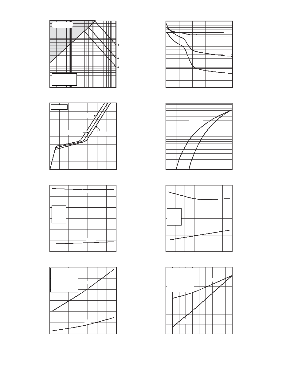
FIGURE 10, MAXIMUM SAFE OPERATING AREA
FIGURE 11, CAPACITANCE vs DRAIN-TO-SOURCE VOLTAGE
Q
g
, TOTAL GATE CHARGE (nC)
V
SD
, SOURCE-TO-DRAIN VOLTAGE (VOLTS)
FIGURE 12, GATE CHARGES vs GATE-TO-SOURCE VOLTAGE
FIGURE 13, SOURCE-DRAIN DIODE FORWARD VOLTAGE
V
GS
, GATE-TO-SOURCE VOLTAGE (VOLTS)
I
D
, DRAIN CURRENT (AMPERES)
I
DR
, REVERSE DRAIN CURRENT (AMPERES)
C
,
CAPACITANCE (pF)
1
10
100
1100
0
10
20
30
40
50
0
20
40
60
80
100
120 140
0.3
0.5
0.7
0.9
1.1
1.3
1.5
52
10
5
1
.5
.1
16
12
8
4
0
TC =+25∞C
TJ =+150∞C
SINGLE PULSE
10mS
1mS
100µS
TJ =+150∞C
TJ =+25∞C
I
D
(A)
I
D
(A)
FIGURE 14, DELAY TIMES vs CURRENT
FIGURE 15, RISE AND FALL TIMES vs CURRENT
I
D
(A)
R
G
, GATE RESISTANCE (Ohms)
FIGURE 16, SWITCHING ENERGY vs CURRENT
FIGURE 17, SWITCHING ENERGY VS. GATE RESISTANCE
V
DD = 733V
R
G = 5
T
J = 125∞C
L = 100µH
E
on
E
off
t
r
t
f
SWITCHING ENERGY (
µ
J)
t
d(on)
and t
d(off)
(ns)
SWITCHING ENERGY (
µ
J)
t
r
and t
f
(ns)
6
8
10
12
14
16
18
20
6
8
10
12
14
16
18
20
6
8
10
12
14
16
18
20
0
5
10 15 20 25 30 35 40 45 50
V
DD = 733V
I
D = 13A
T
J = 125∞C
L = 100µH
E
ON
includes
diode reverse recovery.
t
d(on)
t
d(off)
E
on
E
off
60
50
40
30
20
10
0
1200
1000
800
600
400
200
0
V
DD = 733V
R
G = 5
T
J = 125∞C
L = 100µH
V
DD = 733V
R
G = 5
T
J = 125∞C
L = 100µH
E
ON
includes
diode reverse recovery.
10,000
1,000
100
10
100
10
1
OPERATION HERE
LIMITED BY RDS (ON)
40
30
20
10
0
1400
1200
1000
800
600
400
200
0

050-7187 Rev A 11-2003
Typical Performance Curves
APT1101RBFLL_SFLL
APT's products are covered by one or more of U.S.patents 4,895,810 5,045,903 5,089,434 5,182,234 5,019,522
5,262,336 6,503,786 5,256,583 4,748,103 5,283,202 5,231,474 5,434,095 5,528,058 and foreign patents. US and Foreign patents pending. All Rights Reserved.
15.49 (.610)
16.26 (.640)
5.38 (.212)
6.20 (.244)
6.15 (.242) BSC
4.50 (.177) Max.
19.81 (.780)
20.32 (.800)
20.80 (.819)
21.46 (.845)
1.65 (.065)
2.13 (.084)
1.01 (.040)
1.40 (.055)
3.50 (.138)
3.81 (.150)
2.87 (.113)
3.12 (.123)
4.69 (.185)
5.31 (.209)
1.49 (.059)
2.49 (.098)
2.21 (.087)
2.59 (.102)
0.40 (.016)
0.79 (.031)
Drain
Drain
Source
Gate
5.45 (.215) BSC
Dimensions in Millimeters and (Inches)
2-Plcs.
TO-247 Package Outline
15.95 (.628)
16.05 (.632)
1.22 (.048)
1.32 (.052)
5.45 (.215) BSC
{2 Plcs.}
4.98 (.196)
5.08 (.200)
1.47 (.058)
1.57 (.062)
2.67 (.105)
2.84 (.112)
0.46 (.018) {3 Plcs}
0.56 (.022)
Dimensions in Millimeters (Inches)
Heat Sink (Drain)
and Leads
are Plated
3.81 (.150)
4.06 (.160)
(Base of Lead)
Drain (Heat Sink)
1.98 (.078)
2.08 (.082)
Gate
Drain
Source
0.020 (.001)
0.178 (.007)
1.27 (.050)
1.40 (.055)
11.51 (.453)
11.61 (.457)
13.41 (.528)
13.51 (.532)
Revised
8/29/97
1.04 (.041)
1.15 (.045)
13.79 (.543)
13.99 (.551)
Revised
4/18/95
D
3
PAK Package Outline
Figure 18, Turn-on Switching Waveforms and Definitions
Figure 19, Turn-off Switching Waveforms and Definitions
I
C
D.U.T.
APT15DF100
V
CE
Figure 20, Inductive Switching Test Circuit
V
DD
G
T
J
= 125 C
90%
90%
Gate Voltage
Drain Voltage
Drain Current
10%
0
tf
t
d(off)
Switching Energy
Gate Voltage
Drain Current
Drain Voltage
TJ = 125 C
5 %
90%
10 %
d(on)
t
10 %
5 %
t
r
Switching Energy