
050-7235 Rev A 5-2005
FINAL DATA SHEET WITH MOS 7 FORMAT
600V 20A 0.220
APT20N60BCF
APT20N60SCF
APT20N60BCFG* APT20N60SCFG*
*G Denotes RoHS Compliant, Pb Free Terminal Finish.
MAXIMUM RATINGS
All Ratings: T
C
= 25∞C unless otherwise specified
.
CAUTION: These Devices are Sensitive to Electrostatic Discharge. Proper Handling Procedures Should Be Followed.
Characteristic / Test Conditions
Drain-Source Breakdown Voltage (V
GS
= 0V, I
D
= 250µA)
Drain-Source On-State Resistance
2
(V
GS
= 10V, I
D
= 13A)
Zero Gate Voltage Drain Current (V
DS
= 600V, V
GS
= 0V)
Zero Gate Voltage Drain Current (V
DS
= 600V, V
GS
= 0V, T
C
= 150∞C)
Gate-Source Leakage Current (V
GS
= ±20V, V
DS
= 0V)
Gate Threshold Voltage (V
DS
= V
GS
, I
D
= 1mA)
Symbol
V
DSS
I
D
I
DM
V
GS
P
D
T
J
,T
STG
T
L
dv/dt
I
AR
E
AR
E
AS
Parameter
Drain-Source Voltage
Continuous Drain Current @ T
C
= 25∞C
Continuous Drain Current @ T
C
= 100∞C
Pulsed Drain Current
1
Gate-Source Voltage Continuous
Total Power Dissipation @ T
C
= 25∞C
Linear Derating Factor
Operating and Storage Junction Temperature Range
Lead Temperature: 0.063" from Case for 10 Sec.
Drain-Source Voltage slope (V
DS
= 480V, I
D
= 20A, T
J
= 125∞C)
Avalanche Current
7
Repetitive Avalanche Energy
7
Single Pulse Avalanche Energy
4
UNIT
Volts
Amps
Volts
Watts
W/∞C
∞C
V/ns
Amps
mJ
STATIC ELECTRICAL CHARACTERISTICS
Symbol
BV
DSS
R
DS(on)
I
DSS
I
GSS
V
GS(th)
UNIT
Volts
Ohms
µA
nA
Volts
APT20N60BCF(G)_SCF(G)
600
20
13
60
±30
208
1.67
-55 to 150
260
80
20
1
690
∑ Ultra Low R
DS(ON)
∑ Intrinsic Fast-Recovery Body Diode
∑ Low Miller Capacitance
∑ Extreme Low Reverse Recovery Charge
∑ Ultra Low Gate Charge, Q
g
∑ Ideal For ZVS Applications
∑ Avalanche Energy Rated
∑ Popular TO-247 or Surface Mount D
3
Package
∑ Extreme dv/dt Rated
Super Junction FREDFET
MIN
TYP
MAX
600
0.220
2.1
1700
±100
3
4
5
APT Website - http://www.advancedpower.com
C
Power Semiconductors
O
O L
MOS
G
D
S
"COOLMOSTM comprise a new family of transistors developed by Infineon Technologies AG. "COOLMOS" is a trade-
mark of Infineon Technologies AG."
TO-247
D
3
PAK
050-7235 Rev A 5-2005
DYNAMIC CHARACTERISTICS
APT20N60BCF(G)_SCF(G)
SINGLE PULSE
Z
JC
, THERMAL IMPEDANCE (∞C/W)
10
-5
10
-4
10
-3
10
-2
10
-1
1.0
RECTANGULAR PULSE DURATION (SECONDS)
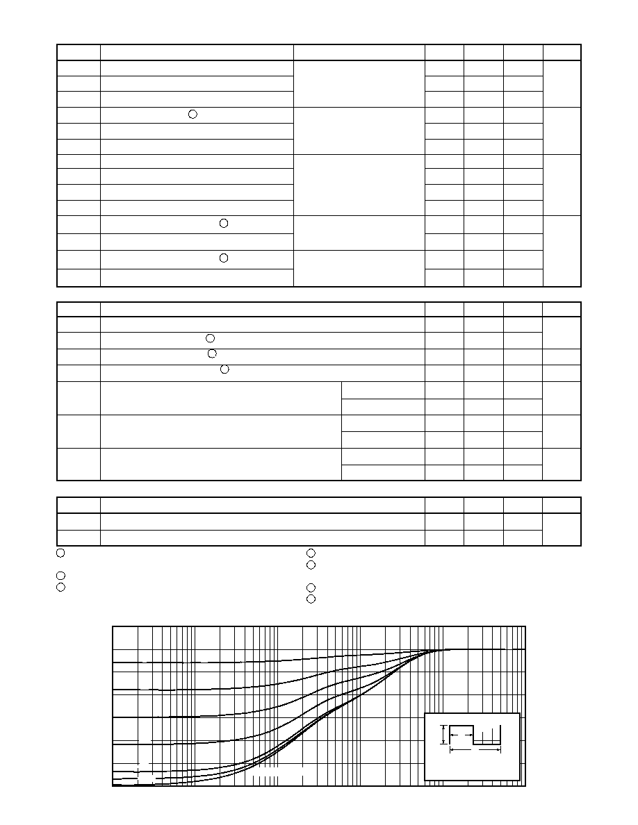
FIGURE 1, MAXIMUM EFFECTIVE TRANSIENT THERMAL IMPEDANCE, JUNCTION-TO-CASE vs PULSE DURATION
0.70
0.60
0.50
0.40
0.30
0.20
0.10
0
0.5
0.1
0.3
0.7
0.9
0.05
FINAL DATA SHEET WITH MOS 7 FORMAT
Peak TJ = PDM x ZJC + TC
Duty Factor D =
t1
/
t2
t2
t1
P
DM
Note:
SOURCE-DRAIN DIODE RATINGS AND CHARACTERISTICS
THERMAL CHARACTERISTICS
Characteristic / Test Conditions
Continuous Source Current (Body Diode)
Pulsed Source Current
1
(Body Diode)
Diode Forward Voltage
2
(V
GS
= 0V, I
S
= -20A)
Peak Diode Recovery
dv
/
dt
5
Reverse Recovery Time
(I
S
= -20A,
di
/
dt
= 100A/µs)
Reverse Recovery Charge
(I
S
= -20A,
di
/
dt
= 100A/µs)
Peak Recovery Current
(I
S
= -20A,
di
/
dt
= 100A/µs)
Symbol
I
S
I
SM
V
SD
dv
/
dt
t
rr
Q
rr
I
RRM
UNIT
Amps
Volts
V/ns
ns
µC
Amps
MIN
TYP
MAX
20
60
1.2
40
180
260
1.4
2.5
15
18
Symbol
R
JC
R
JA
MIN
TYP
MAX
0.60
62
UNIT
∞C/W
Characteristic
Junction to Case
Junction to Ambient
1
Repetitive Rating: Pulse width limited by maximum junction
temperature
2 Pulse Test: Pulse width < 380 µs, Duty Cycle < 2%
3
See MIL-STD-750 Method 3471
APT Reserves the right to change, without notice, the specifications and information contained herein.
T
j
= 25∞C
T
j
= 125∞C
T
j
= 25∞C
T
j
= 125∞C
T
j
= 25∞C
T
j
= 125∞C
Symbol
C
iss
C
oss
C
rss
Q
g
Q
gs
Q
gd
t
d(on)
t
r
t
d(off)
t
f
E
on
E
off
E
on
E
off
Characteristic
Input Capacitance
Output Capacitance
Reverse Transfer Capacitance
Total Gate Charge
3
Gate-Source Charge
Gate-Drain ("Miller") Charge
Turn-on Delay Time
Rise Time
Turn-off Delay Time
Fall Time
Turn-on Switching Energy
6
Turn-off Switching Energy
Turn-on Switching Energy
6
Turn-off Switching Energy
Test Conditions
V
GS
= 0V
V
DS
= 25V
f
= 1 MHz
V
GS
= 10V
V
DD
= 300V
I
D
= 20A
@ 25∞C
RESISTIVE SWITCHING
V
GS
=
15V
V
DD
=
380V
I
D
=
20A
@ 25∞C
R
G
=
3.6
INDUCTIVE SWITCHING @ 25∞C
V
DD
=
400V, V
GS
= 15V
I
D
=
20A, R
G
=
5
INDUCTIVE SWITCHING @ 125∞C
V
DD
=
400V, V
GS
= 15V
I
D
=
20A, R
G
=
5
4
Starting T
j
=
+25∞C, L = 13.80mH, R
G
=
25, Peak I
L
= 10A
5
dv
/
dt
numbers reflect the limitations of the test circuit rather than the
device itself.
I
S
-
I
D
20A
di
/
dt
700A/µs
V
R
480V
T
J
125
∞
C
6 Eon includes diode reverse recovery. See figures 18, 20.
7 Repetitive avalanche causes additional power losses that can be calcu-
lated as
P
AV
= E
AR
*f
MIN
TYP
MAX
2520
670
40
95
18
55
12
15
60
6.4
180
60
315
80
UNIT
pF
nC
ns
µ
J
050-7235 Rev A 5-2005
Typical Performance Curves
APT20N60BCF(G)_SCF(G)
Scope pics are placed with the place command
and then scaled to 50%
Scope pics are placed with the place command
and then scaled to 50%
7V
5.5V
6V
6.5V
V
GS
= 15 &10 V
8V
60
50
40
30
20
10
0
1.40
1.30
1.20
1.10
1.00
0.90
0.80
1.15
1.10
1.05
1.00
0.95
0.90
1.2
1.1
1.0
0.9
0.8
0.7
0.6
V
DS
> I
D(ON)
x R
DS(ON)
MAX.
250µSEC. PULSE TEST
@ <0.5 % DUTY CYCLE
R
DS
(ON), DRAIN-TO-SOURCE ON RESISTANCE
I
D
, DRAIN CURRENT (AMPERES)
I
D
, DRAIN CURRENT (AMPERES)
(NORMALIZED)
V
GS
(TH), THRESHOLD VOLTAGE
BV
DSS
, DRAIN-TO-SOURCE BREAKDOWN
R
DS
(ON), DRAIN-TO-SOURCE ON RESISTANCE
I
D
, DRAIN CURRENT (AMPERES)
(NORMALIZED)
VOLTAGE (NORMALIZED)
V
DS
, DRAIN-TO-SOURCE VOLTAGE (VOLTS)
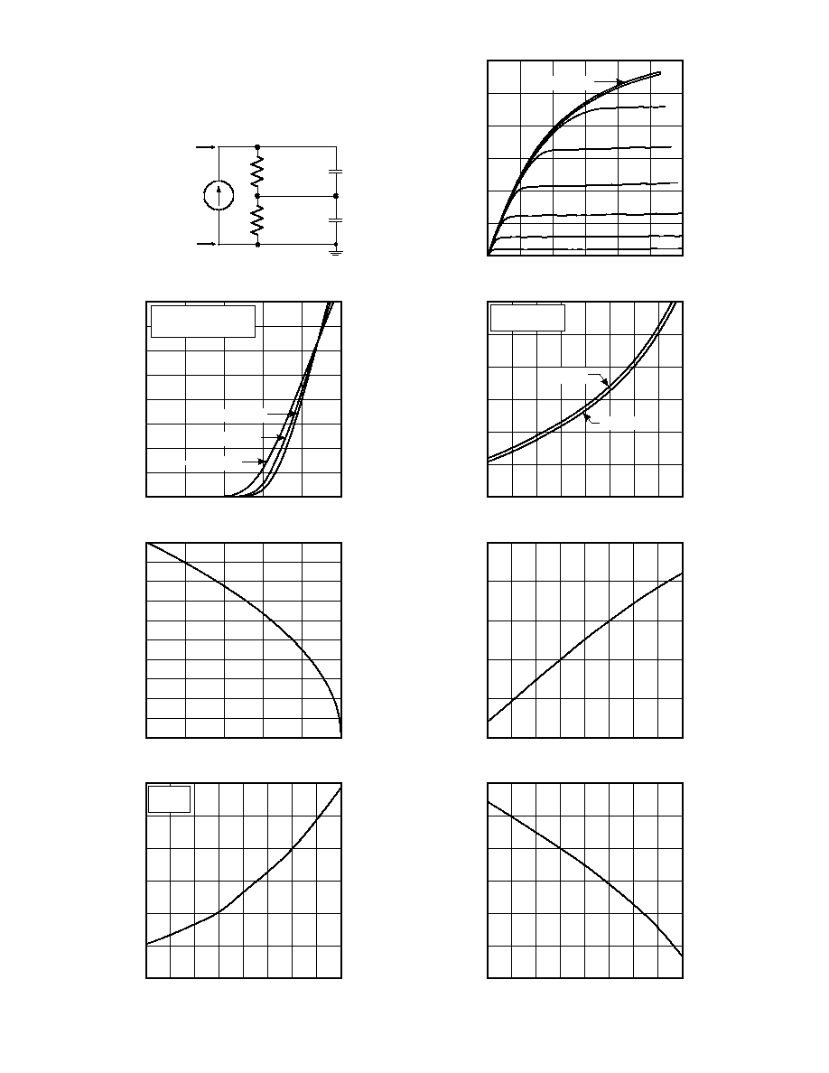
FIGURE 2, TRANSIENT THERMAL IMPEDANCE MODEL
FIGURE 3, LOW VOLTAGE OUTPUT CHARACTERISTICS
V
GS
, GATE-TO-SOURCE VOLTAGE (VOLTS)
I
D
, DRAIN CURRENT (AMPERES)
FIGURE 4, TRANSFER CHARACTERISTICS
FIGURE 5, R
DS
(ON) vs DRAIN CURRENT
T
C
, CASE TEMPERATURE (∞C)
T
J
, JUNCTION TEMPERATURE (∞C)
FIGURE 6, MAXIMUM DRAIN CURRENT vs CASE TEMPERATURE
FIGURE 7, BREAKDOWN VOLTAGE vs TEMPERATURE
T
J
, JUNCTION TEMPERATURE (∞C)
T
C
, CASE TEMPERATURE (∞C)
FIGURE 8, ON-RESISTANCE vs. TEMPERATURE
FIGURE 9, THRESHOLD VOLTAGE vs TEMPERATURE
0
5
10
15
20
25
30
0
2
4
6
8
10
0
5
10 15 20 25
30 35 40
25
50
75
100
125
150
-50 -25
0
25 50 75 100 125 150
-50 -25
0
25 50
75 100 125 150
-50 -25
0
25 50 75 100 125 150
7.5V
T
J
= -55∞C
T
J
= +25∞C
T
J
= +125∞C
NORMALIZED TO
V
GS
= 10V @ 13A
V
GS
=10V
V
GS
=20V
80
70
60
50
40
30
20
10
0
20
18
16
14
12
10
8
6
4
2
0
3.0
2.5
2.0
1.5
1.0
0.5
0
I
D
= 10A
V
GS
= 10V
0.322
0.276
0.00498F
0.0728F
Power
(watts)
RC MODEL
Junction
temp. (∞C)
Case temperature. (∞C)
050-7235 Rev A 5-2005
APT20N60BCF(G)_SCF(G)
Scope pics are placed with the place command
and then scaled to 50%
Scope pics are placed with the place command
and then scaled to 50%
T
C
=+25∞C
T
J
=+150∞C
SINGLE PULSE
OPERATION HERE
LIMITED BY RDS (ON)
C
rss
C
iss
C
oss
V
GS
, GATE-TO-SOURCE VOLTAGE (VOLTS)
I
D
, DRAIN CURRENT (AMPERES)
I
DR
, REVERSE DRAIN CURRENT (AMPERES)
C, CAPACITANCE (pF)
60
10
5
1
.1
16
12
8
4
0
20,000
10,000
1,000
100
10
200
100
10
1
V
DS
, DRAIN-TO-SOURCE VOLTAGE (VOLTS)
V
DS
, DRAIN-TO-SOURCE VOLTAGE (VOLTS)
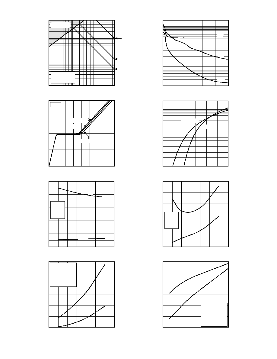
FIGURE 10, MAXIMUM SAFE OPERATING AREA
FIGURE 11, CAPACITANCE vs DRAIN-TO-SOURCE VOLTAGE
Q
g
, TOTAL GATE CHARGE (nC)
V
SD
, SOURCE-TO-DRAIN VOLTAGE (VOLTS)
FIGURE 12, GATE CHARGE vs GATE-TO-SOURCE VOLTAGE
FIGURE 13, SOURCE-DRAIN DIODE FORWARD VOLTAGE
100µS
1mS
10mS
SWITCHING ENERGY (mJ)
t
d(on)
and t
d(off)
(ns)
SWITCHING ENERGY (mJ)
t
r
and t
f
(ns)
E
on
E
off
I
D
(A)
I
D
(A)
FIGURE 14, DELAY TIMES vs CURRENT
FIGURE 15, RISE AND FALL TIMES vs CURRENT
I
D
(A)
R
G
, GATE RESISTANCE (Ohms)
FIGURE 16, SWITCHING ENERGY vs CURRENT
FIGURE 17, SWITCHING ENERGY VS. GATE RESISTANCE
T
J
=+150∞C
T
J
=+25∞C
I
D
= 20A
t
d(on)
t
d(off)
V
DD
= 400V
R
G
= 5
T
J
= 125∞C
L = 100µH
V
DD
= 400V
R
G
= 5
T
J
= 125∞C
L = 100µH
E
on
includes
diode reverse recovery.
V
DD
= 400V
R
G
= 5
T
J
= 125∞C
L = 100µH
t
r
t
f
0
5
10
15
20
25
30
35
0
5
10
15
20
25
30
35
0
5
10
15
20
25
30
35
0
10
20
30
40
50
1
10
100
600
0
10
20
30
40
50
0
20 40 60 80 100 120 140 160
0.3
0.5
0.7
0.9
1.1
1.3
1.5
V
DS
=300V
V
DS
=120V
V
DS
=480V
100
90
80
70
60
50
40
30
20
10
0
600
500
400
300
200
100
0
E
on
E
off
30
25
20
15
10
5
0
600
500
400
300
200
100
0
V
DD
= 400V
I
D
= 20A
T
J
= 125∞C
L = 100µH
E
on
includes
diode reverse recovery.
050-7235 Rev A 5-2005
Typical Performance Curves
APT20N60BCF(G)_SCF(G)
Scope pics are placed with the place command
and then scaled to 50%
Figure 19, Turn-off Switching Waveforms and Definitions
Figure 18, Turn-on Switching Waveforms and Definitions
Drain Current
Drain Voltage
Gate Voltage
T
J
125∞C
10%
t
d(on)
90%
5%
t
r
5%
10%
APT15DQ60
ID
VDS
D.U.T.
V
DD
G
Figure 20, Inductive Switching Test Circuit
T
J
125∞C
10%
0
t
d(off)
t
f
Switching Energy
90%
90%
Drain Voltage
Gate Voltage
Drain Current
Switching Energy
TO-247 Package Outline
D
3
PAK Package Outline
e3
e1 SAC: Tin, Silver, Copper
100% Sn
15.49 (.610)
16.26 (.640)
5.38 (.212)
6.20 (.244)
6.15 (.242) BSC
4.50 (.177) Max.
19.81 (.780)
20.32 (.800)
20.80 (.819)
21.46 (.845)
1.65 (.065)
2.13 (.084)
1.01 (.040)
1.40 (.055)
3.50 (.138)
3.81 (.150)
2.87 (.113)
3.12 (.123)
4.69 (.185)
5.31 (.209)
1.49 (.059)
2.49 (.098)
2.21 (.087)
2.59 (.102)
0.40 (.016)
0.79 (.031)
D
r
a
i
n
Drain
Source
Gate
5.45 (.215) BSC
Dimensions in Millimeters and (Inches)
2-Plcs.
15.95 (.628)
16.05(.632)
1.22 (.048)
1.32 (.052)
5.45 (.215) BSC
{2 Plcs.}
4.98 (.196)
5.08 (.200)
1.47 (.058)
1.57 (.062)
2.67 (.105)
2.84 (.112)
0.46 (.018) {3 Plcs}
0.56 (.022)
Dimensions in Millimeters (Inches)
Heat Sink (Drain)
and Leads
are Plated
3.81 (.150)
4.06 (.160)
(Base of Lead)
D
r
a
i
n
(Heat Sink)
1.98 (.078)
2.08 (.082)
Gate
Drain
Source
0.020 (.001)
0.178 (.007)
1.27 (.050)
1.40 (.055)
11.51 (.453)
11.61 (.457)
13.41 (.528)
13.51(.532)
Revised
8/29/97
1.04 (.041)
1.15(.045)
13.79 (.543)
13.99(.551)
Revised
4/18/95
APT's products are covered by one or more of U.S.patents 4,895,810 5,045,903 5,089,434 5,182,234 5,019,522
5,262,336 6,503,786 5,256,583 4,748,103 5,283,202 5,231,474 5,434,095 5,528,058 and foreign patents. US and Foreign patents pending. All Rights Reserved.