053-4201 Rev B 11-2005
PRODUCT BENEFITS
∑ Low Losses
∑ Low Noise Switching
∑ Cooler Operation
∑ Higher Reliability Systems
∑ Increased System Power
Density
PRODUCT FEATURES
∑ Ultrafast Recovery Times
∑ Soft Recovery Characteristics
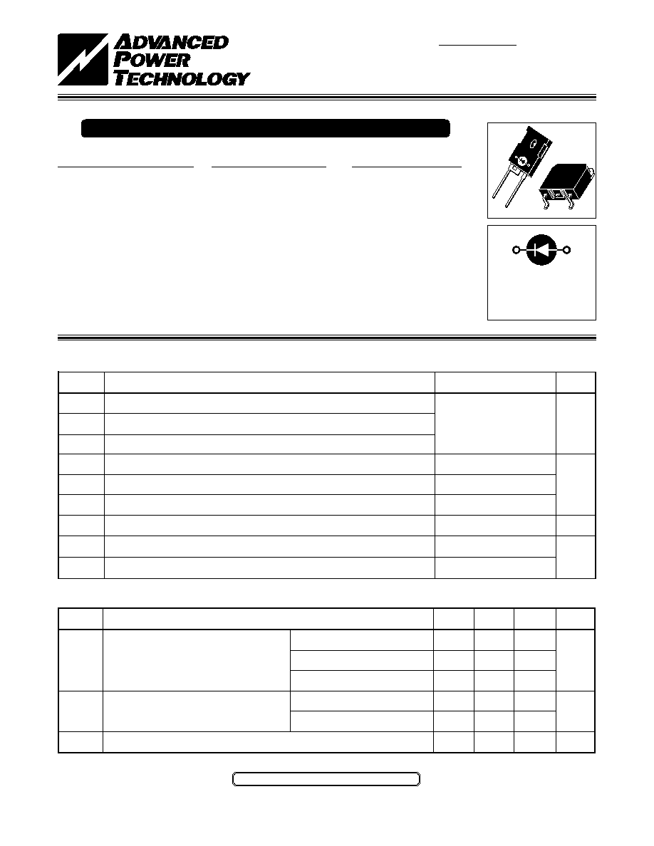
∑ Popular TO-247 Package or
Surface Mount D
3
PAK Package
∑ Low Forward Voltage
∑ Low Leakage Current
∑ Avalanche Energy Rated
PRODUCT APPLICATIONS
∑ Anti-Parallel Diode
-Switchmode Power Supply
-Inverters
∑ Free Wheeling Diode
-Motor Controllers
-Converters
-Inverters
∑ Snubber Diode
∑ PFC
ULTRAFAST SOFT RECOVERY RECTIFIER DIODE
600V 30A
APT30DQ60B
APT30DQ60S
APT30DQ60BG* APT30DQ60SG*
*G Denotes RoHS Compliant, Pb Free Terminal Finish.
MAXIMUM RATINGS
All Ratings: T
C
= 25∞C unless otherwise specified.
Æ
APT Website - http://www.advancedpower.com
STATIC ELECTRICAL CHARACTERISTICS
Symbol
V
F
I
RM
C
T
UNIT
Volts
µA
pF
MIN
TYP
MAX
2.0
2.4
2.4
1.7
25
500
36
Characteristic / Test Conditions
Forward Voltage
Maximum Reverse Leakage Current
Junction Capacitance, V
R
= 200V
I
F
= 30A
I
F
= 60A
I
F
= 30A, T
J
= 125∞C
V
R
= 600V
V
R
= 600V, T
J
= 125∞C
Characteristic / Test Conditions
Maximum D.C. Reverse Voltage
Maximum Peak Repetitive Reverse Voltage
Maximum Working Peak Reverse Voltage
Maximum Average Forward Current (T
C
= 117∞C, Duty Cycle = 0.5)
RMS Forward Current (Square wave, 50% duty)
Non-Repetitive Forward Surge Current (T
J
= 45∞C, 8.3ms)
Avalanche Energy (1A, 40mH)
Operating and StorageTemperature Range
Lead Temperature for 10 Sec.
Symbol
V
R
V
RRM
V
RWM
I
F(AV)
I
F(RMS)
I
FSM
E
AVL
T
J
,T
STG
T
L
UNIT
Volts
Amps
mJ
∞C
APT30DQ60B(G)_S(G)
600
30
51
320
20
-55 to 175
300
1 - Cathode
2 - Anode
Back of Case -Cathode
1
2
TO-2
47
1
2
D
3
PAK
1
2
(S)
(B)
APT30DQ60B(G)_S(G)
DYNAMIC CHARACTERISTICS
053-4201 Rev B 11-2005
APT Reserves the right to change, without notice, the specifications and information contained herein.
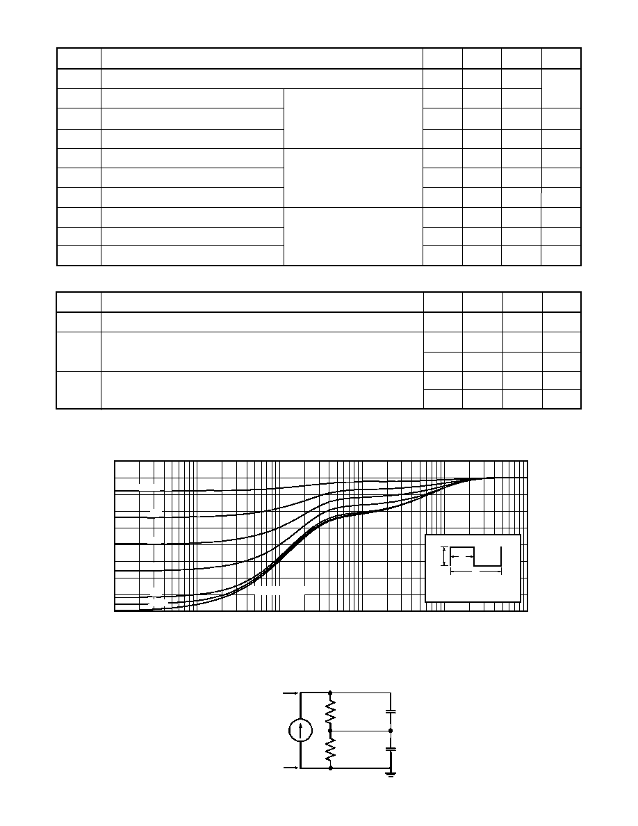
Z
JC
, THERMAL IMPEDANCE (∞C/W)
10
-5
10
-4
10
-3
10
-2
10
-1
1.0
RECTANGULAR PULSE DURATION (seconds)
FIGURE 1a. MAXIMUM EFFECTIVE TRANSIENT THERMAL IMPEDANCE, JUNCTION-TO-CASE vs. PULSE DURATION
0.90
0.80
0.70
0.60
0.50
0.40
0.30
0.20
0.10
0
0.5
SINGLE PULSE
0.1
0.3
0.7
0.05
FIGURE 1b, TRANSIENT THERMAL IMPEDANCE MODEL
Peak TJ = PDM x ZJC + TC
Duty Factor D =
t1
/
t2
t2
t1
P
DM
Note:
MIN
TYP
MAX
-
23
-
30
-
55
-
3
-
-
175
-
485
-
6
-
-
75
-
855
-
22
UNIT
ns
nC
Amps
ns
nC
Amps
ns
nC
Amps
Characteristic
Reverse Recovery Time
Reverse Recovery Time
Reverse Recovery Charge
Maximum Reverse Recovery Current
Reverse Recovery Time
Reverse Recovery Charge
Maximum Reverse Recovery Current
Reverse Recovery Time
Reverse Recovery Charge
Maximum Reverse Recovery Current
Symbol
t
rr
t
rr
Q
rr
I
RRM
t
rr
Q
rr
I
RRM
t
rr
Q
rr
I
RRM
Test Conditions
I
F
= 30A, di
F
/dt = -200A/µs
V
R
= 400V, T
C
= 25∞C
I
F
= 30A, di
F
/dt = -200A/µs
V
R
= 400V, T
C
= 125∞C
I
F
= 30A, di
F
/dt = -1000A/µs
V
R
= 400V, T
C
= 125∞C
I
F
= 1A, di
F
/dt = -100A/µs, V
R
= 30V, T
J
= 25∞C
THERMAL AND MECHANICAL CHARACTERISTICS
Characteristic / Test Conditions
Junction-to-Case Thermal Resistance
Package Weight
Maximum Mounting Torque
Symbol
R
JC
W
T
Torque
MIN
TYP
MAX
.80
0.22
5.9
10
1.1
UNIT
∞C/W
oz
g
lb∑in
N∑m
D = 0.9
0.560
0.240
0.00230
0.284
Power
(watts)
RC MODEL
Junction
temp. (∞C)
Case temperature. (∞C)
053-4201 Rev B 11-2005
APT30DQ60B(G)_S(G)
TYPICAL PERFORMANCE CURVES
T
J
= 125∞C
V
R
= 400V
15A
30A
60A
t
rr
Q
rr
Q
rr
t
rr
I
RRM
200
180
160
140
120
100
80
60
40
20
0
25
20
15
10
5
0
Duty cycle = 0.5
T
J
= 175∞C
0
25
50
75
100
125
150
25
50
75
100
125
150
175
1
10
100 200
60
50
40
30
20
10
0
1.2
1.0
0.8
0.6
0.4
0.2
0.0
200
180
160
140
120
100
80
60
40
20
0
C
J
, JUNCTION CAPACITANCE
K
f
, DYNAMIC PARAMETE
RS
(pF)
(Normalized to 1000A/
µ
s)
I
F(AV)
(A)
T
J
, JUNCTION TEMPERATURE (∞C)
Case Temperature (∞C)
Figure 6. Dynamic Parameters vs. Junction Temperature
Figure 7. Maximum Average Forward Current vs. CaseTemperature
V
R
, REVERSE VOLTAGE (V)
Figure 8. Junction Capacitance vs. Reverse Voltage
100
80
60
40
20
0
1200
1000
800
600
400
200
0
V
F
, ANODE-TO-CATHODE VOLTAGE (V)
-di
F
/dt, CURRENT RATE OF CHANGE(A/µs)
Figure 2. Forward Current vs. Forward Voltage
Figure 3. Reverse Recovery Time vs. Current Rate of Change
-di
F
/dt, CURRENT RATE OF CHANGE (A/µs)
-di
F
/dt, CURRENT RATE OF CHANGE (A/µs)
Figure 4. Reverse Recovery Charge vs. Current Rate of Change
Figure 5. Reverse Recovery Current vs. Current Rate of Change
0
0.5
1.0
1.5
2.0
2.5
3.0
0
200
400
600
800 1000 1200
0
200
400
600
800 1000 1200
0
200
400
600
800 1000 1200
Q
rr
, REVERSE RECOVERY CHARGE
I
F
,
FORWARD CURRENT
(nC)
(A)
I
RRM
, REVERSE RECOVERY CURRENT
t
rr
, REVERSE RECOVERY TIME
(A)
(ns)
T
J
= 175∞C
T
J
= -55∞C
T
J
= 25∞C
T
J
= 125∞C
T
J
= 125∞C
V
R
= 400V
60A
30A
15A
T
J
= 125∞C
V
R
= 400V
60A
15A
30A
APT30DQ60B(G)_S(G)
053-4201 Rev B 11-2005
4
3
1
2
5
5
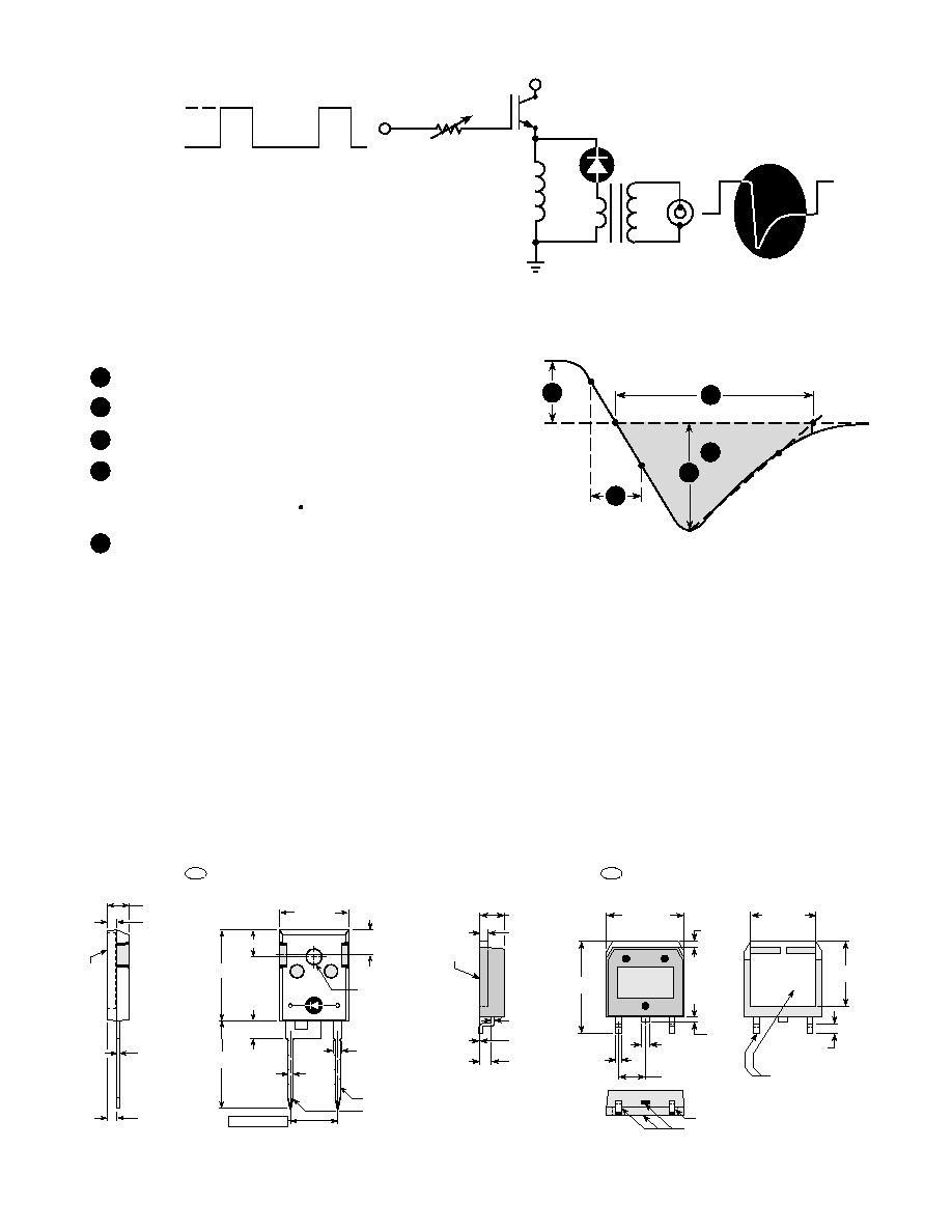
Zero
1
2
3
4
di
F
/dt - Rate of Diode Current Change Through Zero Crossing.
I
F
- Forward Conduction Current
I
RRM
- Maximum Reverse Recovery Current.
trr - Reverse
R
ecovery Time, measured from zero crossing where
diode
Qrr - Area Under the Curve Defined by I
RRM
and trr.
current goes from positive to negative, to the point at which the straight
line through I
RRM
and 0.25 I
RRM
passes through zero.
Figure 9. Diode Test Circuit
Figure 10, Diode Reverse Recovery Waveform and Definitions
0.25 IRRM
PEARSON 2878
CURRENT
TRANSFORMER
di
F
/dt Adjust
30µH
D.U.T.
+18V
0V
trr/Qrr
Waveform
Vr
APT30GT60BR
APT's products are covered by one or more of U.S.patents 4,895,810 5,045,903 5,089,434 5,182,234 5,019,522
5,262,336 6,503,786 5,256,583 4,748,103 5,283,202 5,231,474 5,434,095 5,528,058 and foreign patents. US and Foreign patents pending. All Rights Reserved.
15.85 (.624)
16.05(.632)
18.70 (.736)
19.10 (.752)
1.15 (.045)
1.45 (.057)
5.45 (.215) BSC
(2 Plcs.)
4.90 (.193)
5.10 (.201)
1.45 (.057)
1.60 (.063)
2.70 (.106)
2.90 (.114)
0.40 (.016)
0.65 (.026)
Dimensions in Millimeters (Inches)
Heat Sink (Cathode)
and Leads
are Plated
2.40 (.094)
2.70 (.106)
(Base of Lead)
C
a
t
h
o
d
e
(Heat Sink)
1.90 (.075)
2.10 (.083)
Cathode
Anode
0.020 (.001)
0.250 (.010)
1.20 (.047)
1.40 (.055)
12.40 (.488)
12.70 (.500)
13.30 (.524)
13.60(.535)
1.00 (.039)
1.15(.045)
15.49 (.610)
16.26 (.640)
5.38 (.212)
6.20 (.244)
6.15 (.242) BSC
4.50 (.177) Max.
19.81 (.780)
20.32 (.800)
20.80 (.819)
21.46 (.845)
1.65 (.065)
2.13 (.084)
1.01 (.040)
1.40 (.055)
10.90 (.430) BSC
3.50 (.138)
3.81 (.150)
4.69 (.185)
5.31 (.209)
1.49 (.059)
2.49 (.098)
2.21 (.087)
2.59 (.102)
0.40 (.016)
0.79 (.031)
Dimensions in Millimeters and (Inches)
C
a
t
h
o
d
e
Anode
Cathode
TO-247 Package Outline
D
3
PAK Package Outline
e3
e1 SAC: Tin, Silver, Copper
100% Sn