050-7238 Rev A 2-2006
FINAL DATA SHEET WITH MOS 7 FORMAT
C
Power Semiconductors
O
O L
MOS
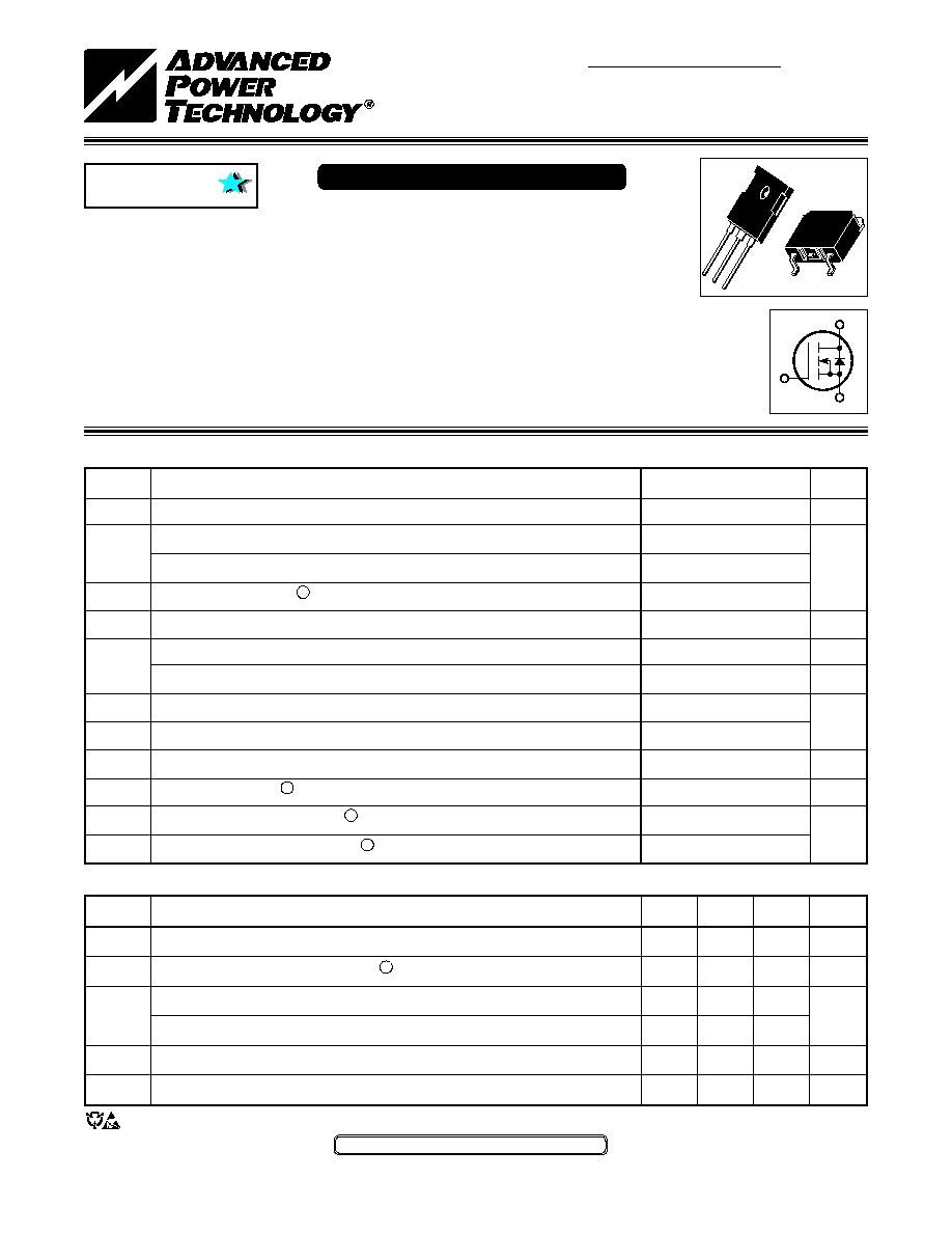
TO-247
D
3
PAK
G
D
S
(S)
(B)
600V 31A 0.100
APT31N60BCS
APT31N60SCS
APT31N60BCSG* APT31N60SCSG*
*G Denotes RoHS Compliant, Pb Free Terminal Finish.
� Ultra Low R
DS(ON)
� Low Miller Capacitance
� Ultra Low Gate Charge, Q
g
� Avalanche Energy Rated
� Extreme dv/dt Rated
� Popular TO-247 or Surface Mount D
3
Package
Super Junction MOSFET
MAXIMUM RATINGS
All Ratings: T
C
= 25�C unless otherwise specified
.
CAUTION: These Devices are Sensitive to Electrostatic Discharge. Proper Handling Procedures Should Be Followed.
Characteristic / Test Conditions
Drain-Source Breakdown Voltage (V
GS
= 0V, I
D
= 250�A)
Drain-Source On-State Resistance
2
(V
GS
= 10V, I
D
= 18A)
Zero Gate Voltage Drain Current (V
DS
= 600V, V
GS
= 0V)
Zero Gate Voltage Drain Current (V
DS
= 600V, V
GS
= 0V, T
C
= 150�C)
Gate-Source Leakage Current (V
GS
= �20V, V
DS
= 0V)
Gate Threshold Voltage (V
DS
= V
GS
, I
D
= 1.2mA)
Symbol
V
DSS
I
D
I
DM
V
GS
P
D
T
J
,T
STG
T
L
dv/dt
I
AR
E
AR
E
AS
Parameter
Drain-Source Voltage
Continuous Drain Current @ T
C
= 25�C
Continuous Drain Current @ T
C
= 100�C
Pulsed Drain Current
1
Gate-Source Voltage Continuous
Total Power Dissipation @ T
C
= 25�C
Linear Derating Factor
Operating and Storage Junction Temperature Range
Lead Temperature: 0.063" from Case for 10 Sec.
MOSFET dv/dt Ruggedness (V
DS
= 480V)
Avalanche Current
2
Repetitive Avalanche Energy
2
Single Pulse Avalanche Energy
3
UNIT
Volts
Amps
Volts
Watts
W/�C
�C
V/ns
Amps
mJ
STATIC ELECTRICAL CHARACTERISTICS
Symbol
V
(BR)DSS
R
DS(on)
I
DSS
I
GSS
V
GS(th)
UNIT
Volts
Ohms
�A
nA
Volts
APT31N60B_SCS(G)
600
31
19
93
�30
255
2.00
-55 to 150
260
50
11
1.2
800
MIN
TYP
MAX
600
0.100
10
TBD
�100
2.1
3
3.9
APT Website - http://www.advancedpower.com
"COOLMOSTM comprise a new family of transistors developed by Infineon Technologies AG. "COOLMOS" is a trade-
mark of Infineon Technologies AG."
050-7238 Rev A 1-2006
SINGLE PULSE
Z
JC
, THERMAL IMPEDANCE (�C/W)
10
-5
10
-4
10
-3
10
-2
10
-1
1.0
RECTANGULAR PULSE DURATION (SECONDS)
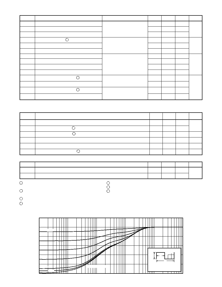
FIGURE 1, MAXIMUM EFFECTIVE TRANSIENT THERMAL IMPEDANCE, JUNCTION-TO-CASE vs PULSE DURATION
0.60
0.50
0.40
0.30
0.20
0.10
0
0.5
0.1
0.3
0.7
D = 0.9
0.05
FINAL DATA SHEET WITH MOS 7 FORMAT
Peak TJ = PDM x ZJC + TC
Duty Factor D =
t1
/
t2
t2
t1
P
DM
Note:
APT Reserves the right to change, without notice, the specifications and information contained herein.
DYNAMIC CHARACTERISTICS
APT31N60B_SCS(G)
Symbol
R
JC
R
JA
MIN
TYP
MAX
0.5
62
UNIT
�C/W
Characteristic
Junction to Case
Junction to Ambient
1
Repetitive Rating: Pulse width limited by maximum junction
temperature
2 Repetitive avalanche causes additional power losses that can
be calculated as
P
AV
= E
AR
*f
3
Starting T
j
=
+25�C, L = 33.23mH, R
G
=
25, Peak I
L
= 11A
4 Pulse Test: Pulse width < 380�s, Duty Cycle < 2%
Symbol
C
iss
C
oss
C
rss
Q
g
Q
gs
Q
gd
t
d(on)
t
r
t
d(off)
t
f
E
on
E
off
E
on
E
off
Characteristic
Input Capacitance
Output Capacitance
Reverse Transfer Capacitance
Total Gate Charge
5
Gate-Source Charge
Gate-Drain ("Miller") Charge
Turn-on Delay Time
Rise Time
Turn-off Delay Time
Fall Time
Turn-on Switching Energy
6
Turn-off Switching Energy
Turn-on Switching Energy
6
Turn-off Switching Energy
Test Conditions
V
GS
= 0V
V
DS
= 25V
f
= 1 MHz
V
GS
= 10V
V
DD
= 400V
I
D
= 18A
@ 25�C
RESISTIVE SWITCHING
V
GS
=
15V
V
DD
=
400V
I
D
=
18A
@ 25�C
R
G
=
3.3
INDUCTIVE SWITCHING @ 25�C
V
DD
=
400V, V
GS
= 15V
I
D
=
18A, R
G
=
4.3
INDUCTIVE SWITCHING @ 125�C
V
DD
=
400V, V
GS
= 15V
I
D
=
18A, R
G
=
4.3
5 See MIL-STD-750 Method 3471
6 Eon includes diode reverse recovery. See figures 18, 20.
7
We do not recommend using this CoolMOSTM product in topologies
that have fee wheeling load current conducted in the body diode that is
hard commutated. The current commutation is very "snappy", resulting in
high di/dt at the completion of commutation, and the likelihood of severe
over-voltage transients due to the resulting high dv/dt.
MIN
TYP
MAX
3055
3260
28
65
85
14
22
10
5
110
5
290
125
170
100
UNIT
pF
nC
ns
�
J
SOURCE-DRAIN DIODE RATINGS AND CHARACTERISTICS
Characteristic / Test Conditions
Continuous Source Current (Body Diode)
Pulsed Source Current
1
(Body Diode)
Diode Forward Voltage
4
(V
GS
= 0V, I
S
= -
18A
)
Reverse Recovery Time (I
S
= -
18A
, dl
S
/dt = 100A/�s)
Reverse Recovery Charge (I
S
= -
18A
, dl
S
/dt = 100A/�s)
Peak Diode Recovery
dv
/
dt
7
UNIT
Amps
Volts
ns
�C
V/ns
MIN
TYP
MAX
18
93
1.2
450
12
4
Symbol
I
S
I
SM
V
SD
t
rr
Q
rr
dv
/
dt
THERMAL CHARACTERISTICS
050-7238 Rev A 1-2006
Typical Performance Curves
APT31N60B_SCS(G)
Scope pics are placed with the place command
and then scaled to 50%
Scope pics are placed with the place command
and then scaled to 50%
5V
5.5V
6.5V
15 & 10V
100
90
80
70
60
50
40
30
20
10
0
1.40
1.30
1.20
1.10
1.00
0.90
0.80
1.15
1.10
1.05
1.00
0.95
0.90
1.15
1.10
1.05
1.00
0.95
0.90
0.85
0.80
0.75
0.70
V
DS
> I
D(ON)
x R
DS(ON)
MAX.
250�SEC. PULSE TEST
@ <0.5 % DUTY CYCLE
R
DS(ON)
, DRAIN-TO-SOURCE ON RESISTANCE
I
D
, DRAIN CURRENT (AMPERES)
I
D
, DRAIN CURRENT (AMPERES)
(NORMALIZED)
V
GS
(TH), THRESHOLD VOLTAGE
BV
DSS
, DRAIN-TO-SOURCE BREAKDOWN
R
DS
(ON), DRAIN-TO-SOURCE ON RESISTANCE
I
D
, DRAIN CURRENT (AMPERES)
(NORMALIZED)
VOLTAGE (NORMALIZED)
V
DS
, DRAIN-TO-SOURCE VOLTAGE (VOLTS)
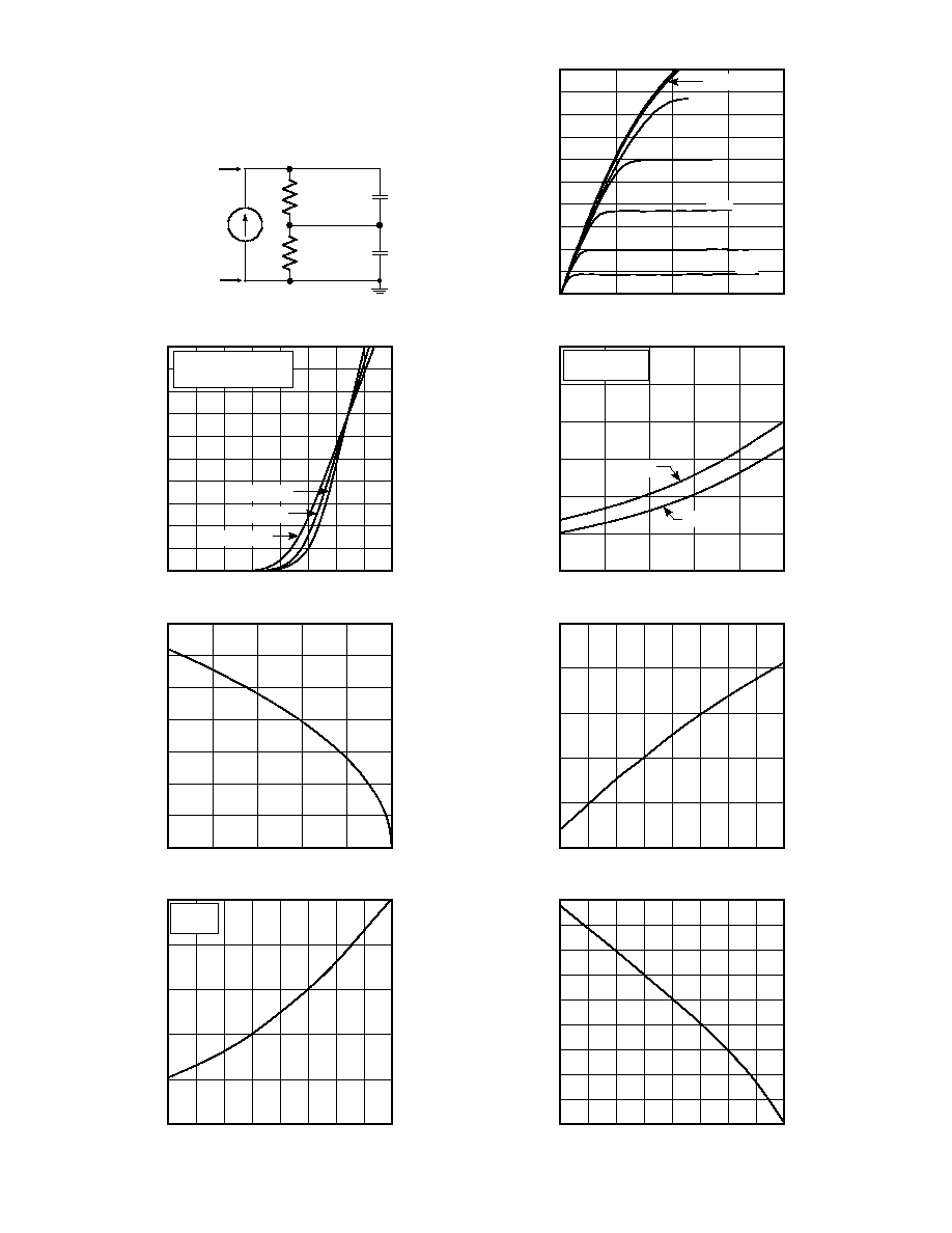
FIGURE 2, TRANSIENT THERMAL IMPEDANCE MODEL
FIGURE 3, LOW VOLTAGE OUTPUT CHARACTERISTICS
V
GS
, GATE-TO-SOURCE VOLTAGE (VOLTS)
I
D
, DRAIN CURRENT (AMPERES)
FIGURE 4, TRANSFER CHARACTERISTICS
FIGURE 5, R
DS
(ON) vs DRAIN CURRENT
T
C
, CASE TEMPERATURE (�C)
T
J
, JUNCTION TEMPERATURE (�C)
FIGURE 6, MAXIMUM DRAIN CURRENT vs CASE TEMPERATURE
FIGURE 7, BREAKDOWN VOLTAGE vs TEMPERATURE
T
J
, JUNCTION TEMPERATURE (�C)
T
C
, CASE TEMPERATURE (�C)
FIGURE 8, ON-RESISTANCE vs. TEMPERATURE
FIGURE 9, THRESHOLD VOLTAGE vs TEMPERATURE
0
5
10
15
20
0
1
2
3
4
5
6
7
8
0
10
20
30
40
50
25
50
75
100
125
150
-50 -25
0
25 50 75 100 125 150
-50 -25
0
25 50
75 100 125 150
-50 -25
0
25 50 75 100 125 150
T
J
= -55�C
T
J
= +25�C
T
J
= +125�C
NORMALIZED TO
V
GS
= 10V @ 18A
V
GS
=10V
V
GS
=20V
100
90
80
70
60
50
40
30
20
10
0
35
30
25
20
15
10
5
0
2.5
2.0
1.5
1.0
0.5
0
I
D
= 18A
V
GS
= 10V
4.5V
0.283
0.216
0.00355
0.727
Power
(watts)
RC MODEL
Junction
temp. (�C)
Case temperature. (�C)
6V
050-7238 Rev A 1-2006
APT31N60B_SCS(G)
Scope pics are placed with the place command
and then scaled to 50%
Scope pics are placed with the place command
and then scaled to 50%
T
C
=+25�C
T
J
=+150�C
SINGLE PULSE
OPERATION HERE
LIMITED BY RDS (ON)
C
rss
C
iss
C
oss
V
GS
, GATE-TO-SOURCE VOLTAGE (VOLTS)
I
D
, DRAIN CURRENT (AMPERES)
I
DR
, REVERSE DRAIN CURRENT (AMPERES)
C, CAPACITANCE (pF)
93
50
10
5
1
.1
16
14
12
10
8
6
4
2
0
20
4
10
4
10
3
10
2
10
1
10
0
200
100
10
1
V
DS
, DRAIN-TO-SOURCE VOLTAGE (VOLTS)
V
DS
, DRAIN-TO-SOURCE VOLTAGE (VOLTS)
FIGURE 10, MAXIMUM SAFE OPERATING AREA
FIGURE 11, CAPACITANCE vs DRAIN-TO-SOURCE VOLTAGE
Q
g
, TOTAL GATE CHARGE (nC)
V
SD
, SOURCE-TO-DRAIN VOLTAGE (VOLTS)
FIGURE 12, GATE CHARGE vs GATE-TO-SOURCE VOLTAGE
FIGURE 13, SOURCE-DRAIN DIODE FORWARD VOLTAGE
100�S
1mS
10mS
SWITCHING ENERGY (mJ)
t
d(on)
and t
d(off)
(ns)
SWITCHING ENERGY (mJ)
t
r
and t
f
(ns)
E
on
E
off
I
D
(A)
I
D
(A)
FIGURE 14, DELAY TIMES vs CURRENT
FIGURE 15, RISE AND FALL TIMES vs CURRENT
I
D
(A)
R
G
, GATE RESISTANCE (Ohms)
FIGURE 16, SWITCHING ENERGY vs CURRENT
FIGURE 17, SWITCHING ENERGY VS. GATE RESISTANCE
T
J
=+150�C
T
J
=+25�C
I
D
= 18A
t
d(on)
t
d(off)
V
DD
= 400V
R
G
= 4.3
T
J
= 125�C
L = 100�H
V
DD
= 400V
R
G
= 4.3
T
J
= 125�C
L = 100�H
E
on
includes
diode reverse recovery.
V
DD
= 400V
R
G
= 4.3
T
J
= 125�C
L = 100�H
t
r
t
f
0
5
10
15
20
25
30
0
5
10
15
20
25
30
0
5
10
15
20
25
30
0 5 10 15 20 25 30 35 40 45 50
1
10
100
600
0
50
100
150
200
0 10 20 30 40 50 60 70 80 90 100
0.3
0.5
0.7
0.9
1.1
1.3
1.5
V
DS
=300V
V
DS
=120V
V
DS
=480V
180
160
140
120
100
80
60
40
20
0
500
400
300
200
100
0
E
on
E
off
45
40
35
30
25
20
15
10
5
0
400
350
300
250
200
150
100
50
0
V
DD
= 400V
I
D
= 18A
T
J
= 125�C
L = 100�H
E
on
includes
diode reverse recovery.
050-7238 Rev A 1-2006
Typical Performance Curves
APT31N60B_SCS(G)
Scope pics are placed with the place command
and then scaled to 50%
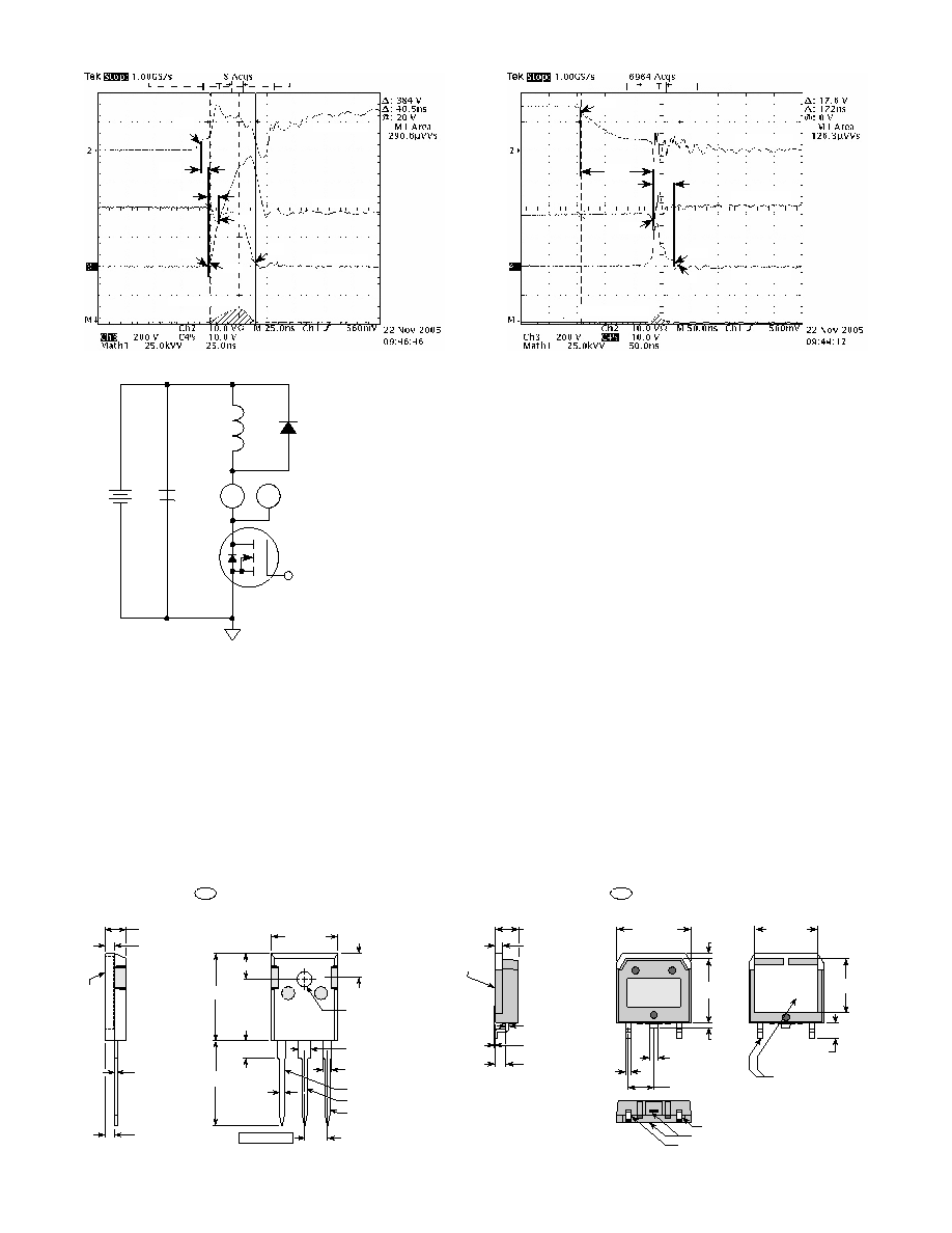
Figure 19, Turn-off Switching Waveforms and Definitions
Figure 18, Turn-on Switching Waveforms and Definitions
Drain Current
Drain Voltage
Gate Voltage
T
J
125�C
10%
t
d(on)
90%
5%
t
r
5%
10%
APT15DQ60
ID
VDS
D.U.T.
V
DD
G
Figure 20, Inductive Switching Test Circuit
T
J
125�C
10%
0
t
d(off)
t
f
Switching Energy
90%
90%
Drain Voltage
Gate Voltage
Drain Current
Switching Energy
TO-247 Package Outline
D
3
PAK Package Outline
e3
e1 SAC: Tin, Silver, Copper
100% Sn
15.49 (.610)
16.26 (.640)
5.38 (.212)
6.20 (.244)
6.15 (.242) BSC
4.50 (.177) Max.
19.81 (.780)
20.32 (.800)
20.80 (.819)
21.46 (.845)
1.65 (.065)
2.13 (.084)
1.01 (.040)
1.40 (.055)
3.50 (.138)
3.81 (.150)
2.87 (.113)
3.12 (.123)
4.69 (.185)
5.31 (.209)
1.49 (.059)
2.49 (.098)
2.21 (.087)
2.59 (.102)
0.40 (.016)
0.79 (.031)
D
r
a
i
n
Drain
Source
Gate
5.45 (.215) BSC
Dimensions in Millimeters and (Inches)
2-Plcs.
15.95 (.628)
16.05(.632)
1.22 (.048)
1.32 (.052)
5.45 (.215) BSC
{2 Plcs.}
4.98 (.196)
5.08 (.200)
1.47 (.058)
1.57 (.062)
2.67 (.105)
2.84 (.112)
0.46 (.018) {3 Plcs}
0.56 (.022)
Dimensions in Millimeters (Inches)
Heat Sink (Drain)
and Leads
are Plated
3.81 (.150)
4.06 (.160)
(Base of Lead)
D
r
a
i
n
(Heat Sink)
1.98 (.078)
2.08 (.082)
Gate
Drain
Source
0.020 (.001)
0.178 (.007)
1.27 (.050)
1.40 (.055)
11.51 (.453)
11.61 (.457)
13.41 (.528)
13.51(.532)
Revised
8/29/97
1.04 (.041)
1.15(.045)
13.79 (.543)
13.99(.551)
Revised
4/18/95
APT's products are covered by one or more of U.S.patents 4,895,810 5,045,903 5,089,434 5,182,234 5,019,522
5,262,336 6,503,786 5,256,583 4,748,103 5,283,202 5,231,474 5,434,095 5,528,058 and foreign patents. US and Foreign patents pending. All Rights Reserved.