050-7406 Rev D 6-2003
APT35GP120B
1200V
The POWER MOS 7
Æ
IGBT is a new generation of high voltage power IGBTs.
Using Punch Through Technology this IGBT is ideal for many high frequency,
high voltage switching applications and has been optimized for high frequency
switchmode power supplies.
∑ Low Conduction Loss
∑ 100 kHz operation @ 800V, 14A
∑ Low Gate Charge
∑ 50 kHz operation @ 800V, 25A
∑ Ultrafast Tail Current shutoff
∑ RBSOA rated
MAXIMUM RATINGS
All Ratings: T
C
= 25∞C unless otherwise specified.
CAUTION: These Devices are Sensitive to Electrostatic Discharge. Proper Handling Procedures Should Be Followed.
APT Website - http://www.advancedpower.com
STATIC ELECTRICAL CHARACTERISTICS
MIN
TYP
MAX
1200
3
4.5
6
3.3
3.9
3
250
2500
±100
Characteristic / Test Conditions
Collector-Emitter Breakdown Voltage (V
GE
= 0V, I
C
= 250µA)
Gate Threshold Voltage (V
CE
= V
GE
, I
C
= 1mA, T
j
= 25∞C)
Collector-Emitter On Voltage (V
GE
= 15V, I
C
= 35A, T
j
= 25∞C)
Collector-Emitter On Voltage (V
GE
= 15V, I
C
= 35A, T
j
= 125∞C)
Collector Cut-off Current (V
CE
= 1200V, V
GE
= 0V, T
j
= 25∞C)
2
Collector Cut-off Current (V
CE
= 1200V, V
GE
= 0V, T
j
= 125∞C)
2
Gate-Emitter Leakage Current (V
GE
= ±20V)
Symbol
BV
CES
V
GE(TH)
V
CE(ON)
I
CES
I
GES
UNIT
Volts
µA
nA
Symbol
V
CES
V
GE
V
GEM
I
C1
I
C2
I
CM
RBSOA
P
D
T
J
,T
STG
T
L
APT35GP120B
1200
±20
±30
96
46
140
140A @ 960V
543
-55 to 150
300
UNIT
Volts
Amps
Watts
∞C
Parameter
Collector-Emitter Voltage
Gate-Emitter Voltage
Gate-Emitter Voltage Transient
Continuous Collector Current @ T
C
= 25∞C
Continuous Collector Current @ T
C
= 110∞C
Pulsed Collector Current
1
@ T
C
= 25∞C
Reverse Bias Safe Operating Area @ T
J
= 150∞C
Total Power Dissipation
Operating and Storage Junction Temperature Range
Max. Lead Temp. for Soldering: 0.063" from Case for 10 Sec.
TO-247
G
C
E
G
C
E
POWER MOS 7
Æ
IGBT
050-7406 Rev D 6-2003
APT35GP120B
DYNAMIC CHARACTERISTICS
Symbol
C
ies
C
oes
C
res
V
GEP
Q
g
Q
ge
Q
gc
RBSOA
t
d(on)
t
r
t
d(off)
t
f
E
on1
E
on2
E
off
t
d(on)
t
r
t
d(off)
t
f
E
on1
E
on2
E
off
Test Conditions
Capacitance
V
GE
= 0V, V
CE
= 25V
f = 1 MHz
Gate Charge
V
GE
= 15V
V
CE
= 600V
I
C
= 35A
T
J
= 150∞C, R
G
= 5
,
V
GE
=
15V, L = 100µH,V
CE
= 960V
Inductive Switching (25∞C)
V
CC
= 600V
V
GE
= 15V
I
C
= 35A
R
G
= 5
T
J
= +25∞C
Inductive Switching (125∞C)
V
CC
= 600V
V
GE
= 15V
I
C
= 35A
R
G
= 5
T
J
= +125∞C
Characteristic
Input Capacitance
Output Capacitance
Reverse Transfer Capacitance
Gate-to-Emitter Plateau Voltage
Total Gate Charge
3
Gate-Emitter Charge
Gate-Collector ("Miller") Charge
Reverse Bias Safe Operating Area
Turn-on Delay Time
Current Rise Time
Turn-off Delay Time
Current Fall Time
Turn-on Switching Energy
4
Turn-on Switching Energy (Diode)
5
Turn-off Switching Energy
6
Turn-on Delay Time
Current Rise Time
Turn-off Delay Time
Current Fall Time
Turn-on Switching Energy
4
Turn-on Switching Energy (Diode)
5
Turn-off Switching Energy
6
MIN
TYP
MAX
3240
248
31
7.5
150
21
62
140
16
20
94
40
750
1305
680
16
20
147
75
750
2132
1744
UNIT
pF
V
nC
A
ns
µ
J
ns
µ
J
UNIT
∞C/W
gm
MIN
TYP
MAX
.23
N/A
5.90
Characteristic
Junction to Case (IGBT)
Junction to Case (DIODE)
Package Weight
Symbol
R
JC
R
JC
W
T
THERMAL AND MECHANICAL CHARACTERISTICS
1 Repetitive Rating: Pulse width limited by maximum junction temperature.
2 For Combi devices, I
ces
includes both IGBT and FRED leakages
3 See MIL-STD-750 Method 3471.
4 E
on1
is the clamped inductive turn-on-energy of the IGBT only, without the effect of a commutating diode reverse recovery current
adding to the IGBT turn-on loss. (See Figure 24.)
5 E
on2
is the clamped inductive turn-on energy that includes a commutating diode reverse recovery current in the IGBT turn-on switching
loss. (See Figures 21, 22.)
6 E
off
is the clamped inductive turn-off energy measured in accordance with JEDEC standard JESD24-1. (See Figures 21, 23.)
APT Reserves the right to change, without notice, the specifications and information contained herein.
050-7406 Rev D 6-2003
TYPICAL PERFORMANCE CURVES
APT35GP120B
V
CE
, COLLECTER-TO-EMITTER VOLTAGE (V)
V
CE
, COLLECTER-TO-EMITTER VOLTAGE (V)
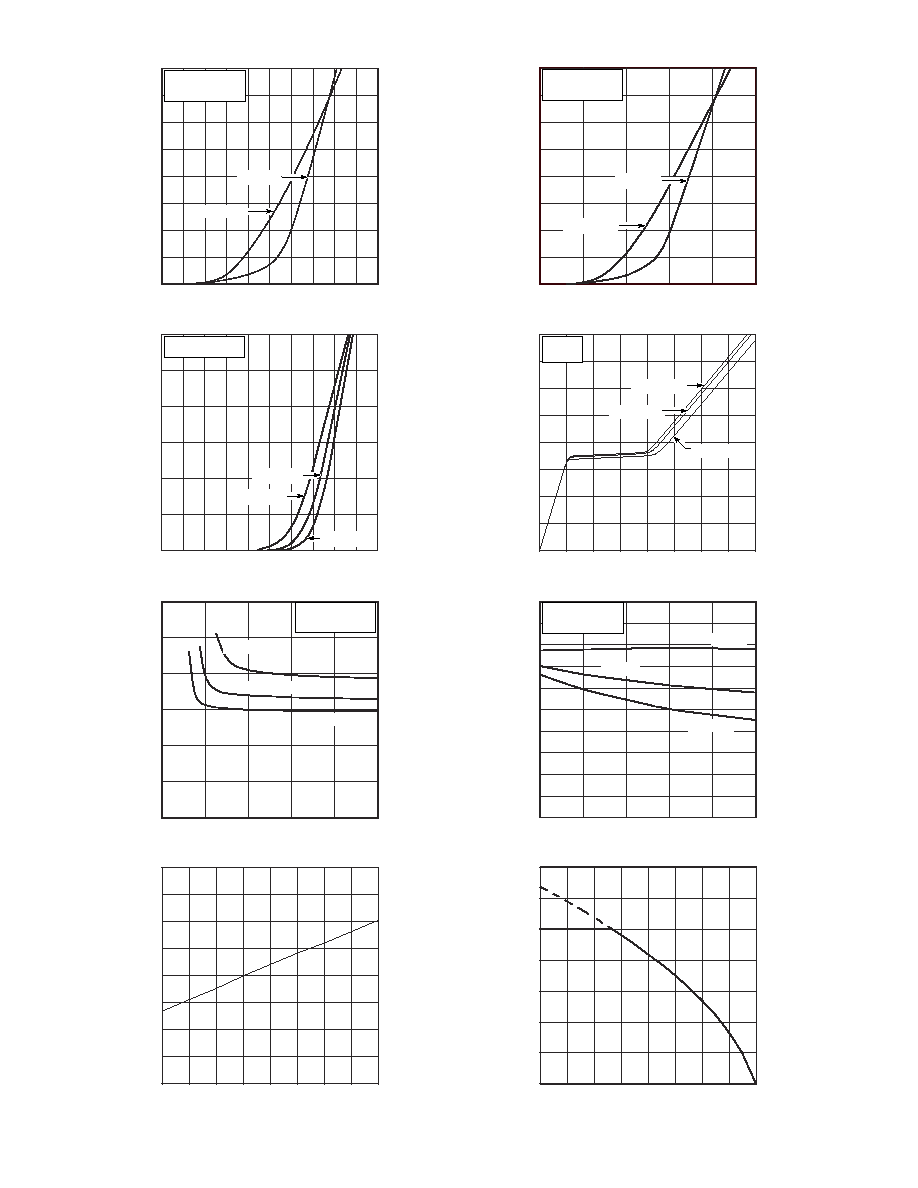
FIGURE 1, Output Characteristics(V
GE
= 15V)
FIGURE 2, Output Characteristics (V
GE
= 10V)
V
GE
, GATE-TO-EMITTER VOLTAGE (V)
GATE CHARGE (nC)
FIGURE 3, Transfer Characteristics
FIGURE 4, Gate Charge
V
GE
, GATE-TO-EMITTER VOLTAGE (V)
T
J
, Junction Temperature (∞C)
FIGURE 5, On State Voltage vs Gate-to- Emitter Voltage
FIGURE 6, On State Voltage vs Junction Temperature
T
J
, JUNCTION TEMPERATURE (∞C)
T
C
, CASE TEMPERATURE (∞C)
FIGURE 7, Breakdown Voltage vs. Junction Temperature
FIGURE 8, DC Collector Current vs Case Temperature
BV
CES
, COLLECTOR-TO-EMITTER BREAKDOWN
V
CE
, COLLECTOR-TO-EMITTER VOLTAGE (V)
I
C
, COLLECTOR CURRENT (A)
I
C
, COLLECTOR CURRENT (A)
VOLTAGE (NORMALIZED)
I
C,
DC COLLECTOR CURRENT(A)
V
CE
, COLLECTOR-TO-EMITTER VOLTAGE (V)
V
GE
, GATE-TO-EMITTER VOLTAGE (V)
I
C
, COLLECTOR CURRENT (A)
VGE = 15V.
250µs PULSE TEST
<0.5 % DUTY CYCLE
T
C
=25∞C
TJ = 25∞C.
250µs PULSE TEST
<0.5 % DUTY CYCLE
VGE = 10V.
250µs PULSE TEST
<0.5 % DUTY CYCLE
VGE = 15V.
250µs PULSE TEST
<0.5 % DUTY CYCLE
TJ = 25∞C
TJ = 125∞C
TJ = -55∞C
IC = 35A
TJ = 25∞C
T
C
=125∞C
T
C
=25∞C
T
C
=125∞C
V
CE
= 960V
V
CE
= 600V
V
CE
= 240V
250µs PULSE TEST
<0.5 % DUTY CYCLE
I
C=
17.5A
I
C=
35A
I
C=
70A
I
C=
70A
I
C=
17.5A
I
C=
35A
80
70
60
50
40
30
20
10
0
120
100
80
60
40
20
0
6
5
4
3
2
1
0
1.2
1.15
1.1
1.05
1.0
0.95
0.90
0.85
0.8
0
1
2
3
4
5
0
1
2
3
4
5
0
1
2
3
4
5
6
7
8
9
10
0
20
40
60
80
100 120 140 160
6
8
10
12
14
16
0
25
50
75
100
125
-50
-25
0
25
50
75 100 125 150
-50
-25
0
25
50
75 100 125 150
80
70
60
50
40
30
20
10
0
16
14
12
10
8
6
4
2
0
5
4.5
4
3.5
3
2.5
2
1.5
1
0.5
0
140
120
100
80
60
40
20
0
050-7406 Rev D 6-2003
APT35GP120B
T
J
=
125∞C, V
GE
=
10V
or 15V
T
J
=
25∞C, V
GE
=
10V
or 15V
V
GE
=
10V,T
J
=125∞C
V
GE
= 15V
V
GE
= 10V
V
GE
=15V,T
J
=125∞C
T
J
=
125∞C, V
GE
=
10V
or 15V
T
J
=
25∞C, V
GE
=
10V
or 15V
I
CE
, COLLECTOR TO EMITTER CURRENT (A)
I
CE
, COLLECTOR TO EMITTER CURRENT (A)
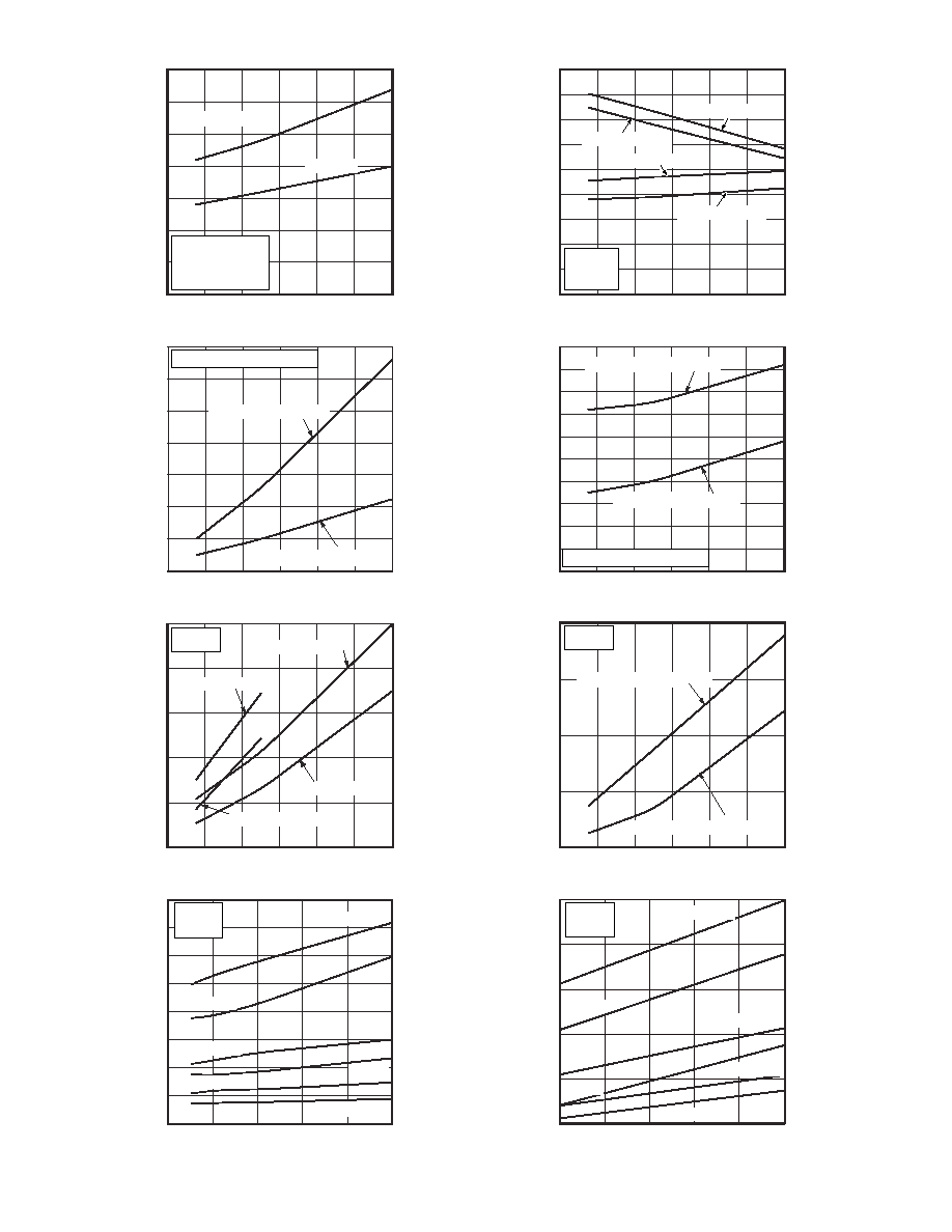
FIGURE 9, Turn-On Delay Time vs Collector Current
FIGURE 10, Turn-Off Delay Time vs Collector Current
I
CE
, COLLECTOR TO EMITTER CURRENT (A)
I
CE
, COLLECTOR TO EMITTER CURRENT (A)
FIGURE 11, Current Rise Time vs Collector Current
FIGURE 12, Current Fall Time vs Collector Current
I
CE
, COLLECTOR TO EMITTER CURRENT (A)
I
CE
, COLLECTOR TO EMITTER CURRENT (A)
FIGURE 13, Turn-On Energy Loss vs Collector Current
FIGURE 14, Turn Off Energy Loss vs Collector Current
R
G
, GATE RESISTANCE (OHMS)
T
J
, JUNCTION TEMPERATURE (∞C)
FIGURE 15, Switching Energy Losses vs. Gate Resistance
FIGURE 16, Switching Energy Losses vs Junction Temperature
V
GE
=15V,T
J
=25∞C
V
GE
=
10V,T
J
=25∞C
10
20
30
40
50
60
70
10
20
30
40
50
60
70
10
20
30
40
50
60
70
10
20
30
40
50
60
70
10
20
30
40
50
60
70
10
20
30
40
50
60
70
0
10
20
30
40
50
0
25
50
75
100
125
180
160
140
120
100
80
60
40
20
0
100
90
80
70
60
50
40
30
20
10
0
4000
3000
2000
1000
0
5000
4000
3000
2000
1000
0
T
J
=
125∞C,V
GE
=
15V
T
J
=
25∞C,V
GE
=
15V
T
J
=
125∞C,V
GE
=
10V
E
on2
35A
E
on2
17.5A
E
off
17.5A
E
off
17.5A
E
off
35A
E
off
70A
E
on2
35A
E
on2
70A
E
on2
17.5A
T
J
= 25 or
125∞C,V
GE
=
10V
T
J
=
25 or125∞C,V
GE
=
10V
E
on2
70A
E
off
70A
E
off
35A
T
J
=
25∞C,V
GE
=
10V
V
CE
= 600V
R
G
= 5
L = 100 µH
R
G
=
5
, L
=
100
µ
H, V
CE
=
600V
VCE = 600V
VGE = +15V
RG = 5
SWITCHING ENERGY LOSSES (µJ)
E
ON2
, TURN ON ENERGY LOSS (µJ)
t
r,
RISE TIME (ns)
t
d(ON)
, TURN-ON DELAY TIME (ns)
SWITCHING ENERGY LOSSES (µJ)
E
OFF
, TURN OFF ENERGY LOSS (µJ)
t
f,
FALL TIME (ns)
t
d
(OFF)
, TURN-OFF DELAY TIME (ns)
VCE = 600V
VGE = +15V
TJ = 125
∞
C
VCE = 600V
RG = 5
VCE = 600V
RG = 5
V
CE
= 600V
T
J
= 25∞C, T
J
=125∞C
R
G
= 5
L = 100 µH
R
G
=
5
, L
=
100
µ
H, V
CE
=
600V
35
30
25
20
15
10
5
0
140
120
100
80
60
40
20
0
5000
4000
3000
2000
1000
0
8000
7000
6000
5000
4000
3000
2000
1000
0
050-7406 Rev D 6-2003
TYPICAL PERFORMANCE CURVES
APT35GP120B
Note:
Duty Factor D = t1/t2
Peak TJ = PDM x Z
JC + TC
t1
t2
P
DM
RECTANGULAR PULSE DURATION (SECONDS)
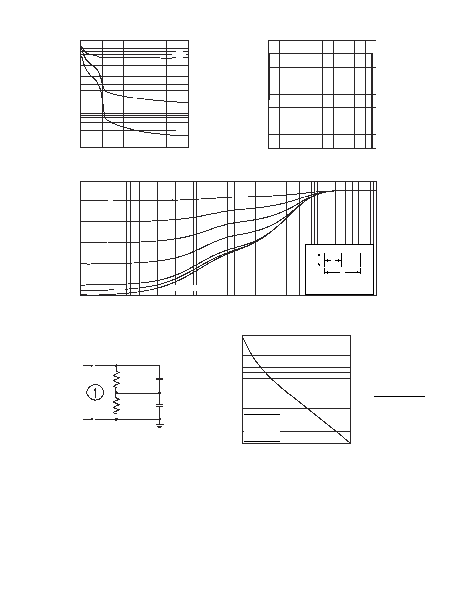
Figure 19, Maximum Effective Transient Thermal Impedance, Junction-To-Case vs Pulse Duration
10
-5
10
-4
10
-3
10
-2
10
-1
1.0
10,000
5,000
1,000
500
100
50
10
160
140
120
100
80
60
40
20
0
C, CAPACITANCE (
P
F)
I
C
, COLLECTOR CURRENT (A)
V
CE
, COLLECTOR-TO-EMITTER VOLTAGE (VOLTS)
V
CE
, COLLECTOR TO EMITTER VOLTAGE
Figure 17, Capacitance vs Collector-To-Emitter Voltage
Figure 18, Reverse Bias Safe Operating Area
0
10
20
30
40
50
0 100 200 300 400 500 600 700 800 900 1000
Cres
Cies
Coes
FIGURE 19B, TRANSIENT THERMAL IMPEDANCE MODEL
0.25
0.20
0.15
0.10
0.05
0
Z
JC
, THERMAL IMPEDANCE (∞C/W)
0.3
0.9
0.7
0.1
0.05
0.5
SINGLE PULSE
0.0896
0.140
0.0108F
0.228F
Power
(Watts)
RC MODEL
Junction
temp. ( "C)
Case temperature
max
max1
max 2
max1
d (on )
r
d(off )
f
diss
cond
max 2
on 2
off
J
C
diss
JC
F
min(f
, f
)
0.05
f
t
t
t
t
P
P
f
E
E
T
T
P
R
=
=
+ +
+
-
=
+
-
=
max
max1
max 2
max1
d (on )
r
d(off )
f
diss
cond
max 2
on 2
off
J
C
diss
JC
F
min(f
, f
)
0.05
f
t
t
t
t
P
P
f
E
E
T
T
P
R
=
=
+ +
+
-
=
+
-
=
F
MAX
, OPERATING FREQUENCY (kHz)
I
C
, COLLECTOR CURRENT (A)
Figure 20, Operating Frequency vs Collector
Current
180
100
50
10
7
10
20
30
40
50
60
70
TJ = 125
∞
C
TC = 75
∞
C
D = 50 %
VCE = 800V
RG = 5
050-7406 Rev D 6-2003
APT35GP120B
T0-247 Package Outline
15.49 (.610)
16.26 (.640)
5.38 (.212)
6.20 (.244)
6.15 (.242) BSC
4.50 (.177) Max.
19.81 (.780)
20.32 (.800)
20.80 (.819)
21.46 (.845)
1.65 (.065)
2.13 (.084)
1.01 (.040)
1.40 (.055)
3.50 (.138)
3.81 (.150)
2.87 (.113)
3.12 (.123)
4.69 (.185)
5.31 (.209)
1.49 (.059)
2.49 (.098)
2.21 (.087)
2.59 (.102)
0.40 (.016)
0.79 (.031)
Collector
Collector
Emitter
Gate
5.45 (.215) BSC
Dimensions in Millimeters and (Inches)
2-Plcs.
*DRIVER SAME TYPE AS D.U.T.
I
C
V
CLAMP
100uH
V
TEST
A
A
B
D.U.T.
DRIVER*
V
CE
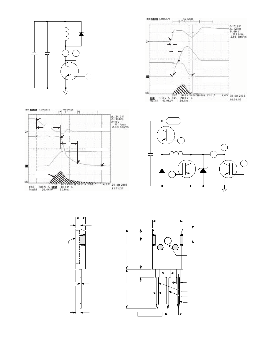
Figure 24,
E
ON1
Test Circuit
Figure 23, Turn-off Switching Waveforms and Definitions
Figure 22, Turn-on Switching Waveforms and Definitions
T
J
= 125 C
Gate Voltage
Collector Voltage
Collector Current
0
10%
t
f
90%
90%
t
d(off)
Switching
Energy
Collector Voltage
Collector Current
T
J
= 125 C
Gate Voltage
Switching Energy
10%
t
r
90%
5%
10%
5 %
t
d(on)
APT's products are covered by one or more of U.S.patents 4,895,810 5,045,903 5,089,434 5,182,234 5,019,522
5,262,336 6,503,786 5,256,583 4,748,103 5,283,202 5,231,474 5,434,095 5,528,058 and foreign patents. US and Foreign patents pending. All Rights Reserved.
I
C
A
D.U.T.
APT30DF120
V
CE
Figure 21, Inductive Switching Test Circuit
V
CC