052-6283 Rev A 3-2006
APT50GF120JRDQ3
TYPICAL PERFORMANCE CURVES
MAXIMUM RATINGS
All Ratings: T
C
= 25∞C unless otherwise specified.
STATIC ELECTRICAL CHARACTERISTICS
Characteristic / Test Conditions
Collector-Emitter Breakdown Voltage (V
GE
= 0V, I
C
= 750µA)
Gate Threshold Voltage (V
CE
= V
GE
, I
C
= 700µA, T
j
= 25∞C)
Collector-Emitter On Voltage (V
GE
= 15V, I
C
= 75A, T
j
= 25∞C)
Collector-Emitter On Voltage (V
GE
= 15V, I
C
= 75A, T
j
= 125∞C)
Collector Cut-off Current (V
CE
= 1200V, V
GE
= 0V, T
j
= 25∞C)
2
Collector Cut-off Current (V
CE
= 1200V, V
GE
= 0V, T
j
= 125∞C)
2
Gate-Emitter Leakage Current (V
GE
= ±20V)
Symbol
V
(BR)CES
V
GE(TH)
V
CE(ON)
I
CES
I
GES
Units
Volts
mA
nA
Symbol
V
CES
V
GE
I
C1
I
C2
I
CM
SSOA
P
D
T
J
,T
STG
T
L
APT50GF120JRDQ3
1200
±30
120
64
225
225A @ 1200V
521
-55 to 150
300
UNIT
Volts
Amps
Watts
∞C
Parameter
Collector-Emitter Voltage
Gate-Emitter Voltage
Continuous Collector Current @ T
C
= 25∞C
Continuous Collector Current @ T
C
= 100∞C
Pulsed Collector Current
1
Switching Safe Operating Area @ T
J
= 150∞C
Total Power Dissipation
Operating and Storage Junction Temperature Range
Max. Lead Temp. for Soldering: 0.063" from Case for 10 Sec.
APT Website - http://www.advancedpower.com
CAUTION: These Devices are Sensitive to Electrostatic Discharge. Proper Handling Procedures Should Be Followed.
MIN
TYP
MAX
1200
4.5
5.5
6.5
2.5
3.0
3.1
0.75
5.5
±100
The Fast IGBT is a new generation of high voltage power IGBTs. Using Non-Punch through
technology, the Fast IGBT combined with an APT free wheeling Ultra Fast Recovery Epi-
taxial Diode (FRED) offers superior ruggedness and fast switching speed.
∑ Low Forward Voltage Drop
∑ High Freq. Switching to 20KHz
∑ RBSOA and SCSOA Rated
∑ Ultra Low Leakage Current
∑ Ultrafast Soft Recovery Anti-parallel Diode
FAST IGBT & FRED
Æ
SO
T-2
27
ISOTOP
Æ
file # E145592
"UL Recognized"
G
E
E
C
C
E
G
1200V
APT50GF120JRDQ3
052-6283 Rev A 3-2006
APT50GF120JRDQ3
DYNAMIC CHARACTERISTICS
Symbol
C
ies
C
oes
C
res
V
GEP
Q
g
Q
ge
Q
gc
SSOA
t
d(on)
t
r
t
d(off)
t
f
E
on1
E
on2
E
off
t
d(on)
t
r
t
d(off)
t
f
E
on1
E
on2
E
off
Test Conditions
Capacitance
V
GE
= 0V, V
CE
= 25V
f = 1 MHz
Gate Charge
V
GE
= 15V
V
CE
= 600V
I
C
= 75A
T
J
= 150∞C, R
G
= 1.0, V
GE
=
15V, L = 100µH,V
CE
= 1200V
Inductive Switching (25∞C)
V
CC
= 800V
V
GE
= 15V
I
C
= 75A
R
G
= 1.0
T
J
= +25∞C
Inductive Switching (125∞C)
V
CC
= 800V
V
GE
= 15V
I
C
= 75A
R
G
= 1.0
T
J
= +125∞C
Characteristic
Input Capacitance
Output Capacitance
Reverse Transfer Capacitance
Gate-to-Emitter Plateau Voltage
Total Gate Charge
3
Gate-Emitter Charge
Gate-Collector ("Miller") Charge
Switching Safe Operating Area
Turn-on Delay Time
Current Rise Time
Turn-off Delay Time
Current Fall Time
Turn-on Switching Energy
4
Turn-on Switching Energy (Diode)
5
Turn-off Switching Energy
6
Turn-on Delay Time
Current Rise Time
Turn-off Delay Time
Current Fall Time
Turn-on Switching Energy
4
4
Turn-on Switching Energy (Diode)
5
5
Turn-off Switching Energy
6
MIN
TYP
MAX
5320
555
300
10.0
495
50
290
225
36
70
355
65
7965
9895
4340
36
70
410
110
7890
14110
6040
UNIT
pF
V
nC
A
ns
µ
J
ns
µ
J
THERMAL AND MECHANICAL CHARACTERISTICS
UNIT
∞C/W
gm
Volts
MIN
TYP
MAX
.24
.56
29.2
2500
Characteristic
Junction to Case
(IGBT)
Junction to Case
(DIODE)
Package Weight
RMS Voltage
(50-60hHz Sinusoidal Wavefomr Ffrom Terminals to Mounting Base for 1 Min.)
Symbol
R
JC
R
JC
W
T
V
Isolation
1
Repetitive Rating: Pulse width limited by maximum junction temperature.
2
For Combi devices, I
ces
includes both IGBT and FRED leakages
3
See MIL-STD-750 Method 3471.
4
E
on1
is the clamped inductive turn-on energy of the IGBT only, without the effect of a commutating diode reverse recovery current
adding to the IGBT turn-on loss. Tested in inductive switching test circuit shown in figure 21, but with a Silicon Carbide diode.
5
E
on2
is the clamped inductive turn-on energy that includes a commutating diode reverse recovery current in the IGBT turn-on switching
loss. (See Figures 21, 22.)
6
E
off
is the clamped inductive turn-off energy measured in accordance with JEDEC standard JESD24-1. (See Figures 21, 23.)
APT Reserves the right to change, without notice, the specifications and information contained herein.
052-6283 Rev A 3-2006
APT50GF120JRDQ3
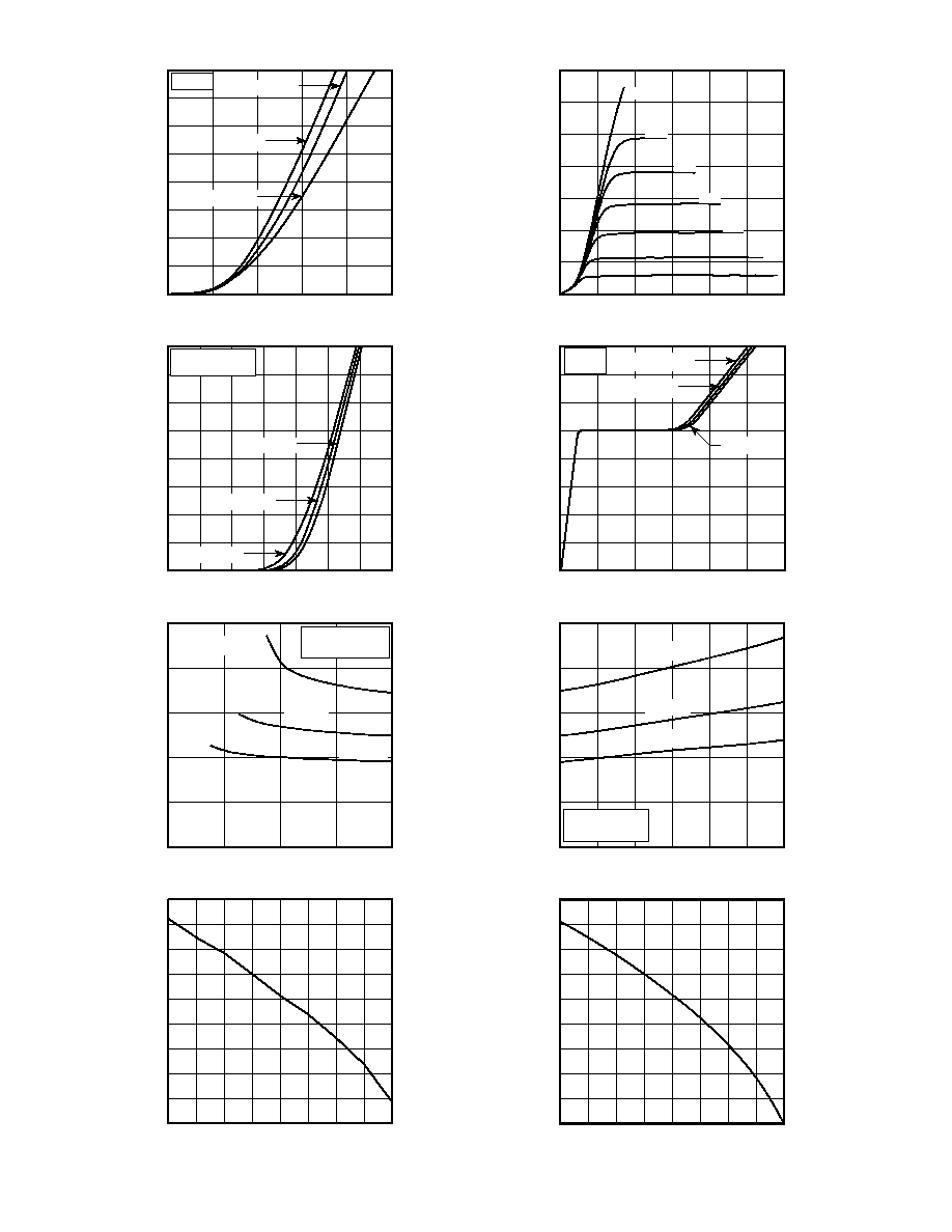
TYPICAL PERFORMANCE CURVES
V
GS(TH)
, THRESHOLD VOLTAGE
V
CE
, COLLECTOR-TO-EMITTER VOLTAGE (V)
I
C
, COLLECTOR CURRENT (A)
I
C
, COLLECTOR CURRENT (A)
(NORMALIZED)
I
C,
DC COLLECTOR CURRENT(A)
V
CE
, COLLECTOR-TO-EMITTER VOLTAGE (V)
V
GE
, GATE-TO-EMITTER VOLTAGE (V)
I
C
, COLLECTOR CURRENT (A)
250µs PULSE
TEST<0.5 % DUTY
CYCLE
160
140
120
100
80
60
40
20
0
160
140
120
100
80
60
40
20
0
5
4
3
2
1
0
1.15
1.10
1.05
1.00
0.95
0.90
0.85
0.80
0.75
0.70
0
1
2
3
4
5
0
5
10
15
20
25
30
0
2
4
6
8
10
12
14
0
100
200
300
400
500
600
8
10
12
14
16
0
25
50
75
100
125
150
-50 -25
0
25 50 75 100 125 150
-50 -25
0
25 50 75 100 125 150
350
300
250
200
150
100
50
0
16
14
12
10
8
6
4
2
0
5
4
3
2
1
0
180
160
140
120
100
80
60
40
20
0
V
CE
, COLLECTER-TO-EMITTER VOLTAGE (V)
V
CE
, COLLECTER-TO-EMITTER VOLTAGE (V)
FIGURE 1, Output Characteristics(T
J
= 25∞C)
FIGURE 2, Output Characteristics (T
J
= 125∞C)
V
GE
, GATE-TO-EMITTER VOLTAGE (V)
GATE CHARGE (nC)
FIGURE 3, Transfer Characteristics
FIGURE 4, Gate Charge
V
GE
, GATE-TO-EMITTER VOLTAGE (V)
T
J
, Junction Temperature (∞C)
FIGURE 5, On State Voltage vs Gate-to- Emitter Voltage
FIGURE 6, On State Voltage vs Junction Temperature
T
J
, JUNCTION TEMPERATURE (∞C)
T
C
, CASE TEMPERATURE (∞C)
FIGURE 7, Threshold Voltage vs. Junction Temperature
FIGURE 8, DC Collector Current vs Case Temperature
15V
12V
11V
9V
13V
8V
V
GE
= 15V.
250µs PULSE TEST
<0.5 % DUTY CYCLE
T
J
= 125∞C
T
J
= 25∞C
T
J
= -55∞C
T
J
= 125∞C
T
J
= 25∞C
T
J
= -55∞C
V
GE
= 15V
V
CE
= 960V
V
CE
= 600V
V
CE
= 240V
I
C
= 75A
T
J
= 25∞C
T
J
= 25∞C.
250µs PULSE TEST
<0.5 % DUTY CYCLE
10V
I
C
= 150A
I
C
= 75A
I
C
= 37.5A
I
C
= 150A
I
C
= 75A
I
C
= 37.5A
052-6283 Rev A 3-2006
APT50GF120JRDQ3
V
GE
=15V,T
J
=125∞C
V
GE
=15V,T
J
=25∞C
V
CE
=
800V
R
G
=
1.0
L = 100µH
SWITCHING ENERGY LOSSES (mJ)
E
ON2
, TURN ON ENERGY LOSS (mJ)
t
r,
RISE TIME (ns)
t
d(ON)
, TURN-ON DELAY TIME (ns)
SWITCHING ENERGY LOSSES (mJ)
E
OFF
, TURN OFF ENERGY LOSS (mJ)
t
f,
FALL TIME (ns)
t
d
(OFF)
, TURN-OFF DELAY TIME (ns)
I
CE
, COLLECTOR TO EMITTER CURRENT (A)
I
CE
, COLLECTOR TO EMITTER CURRENT (A)
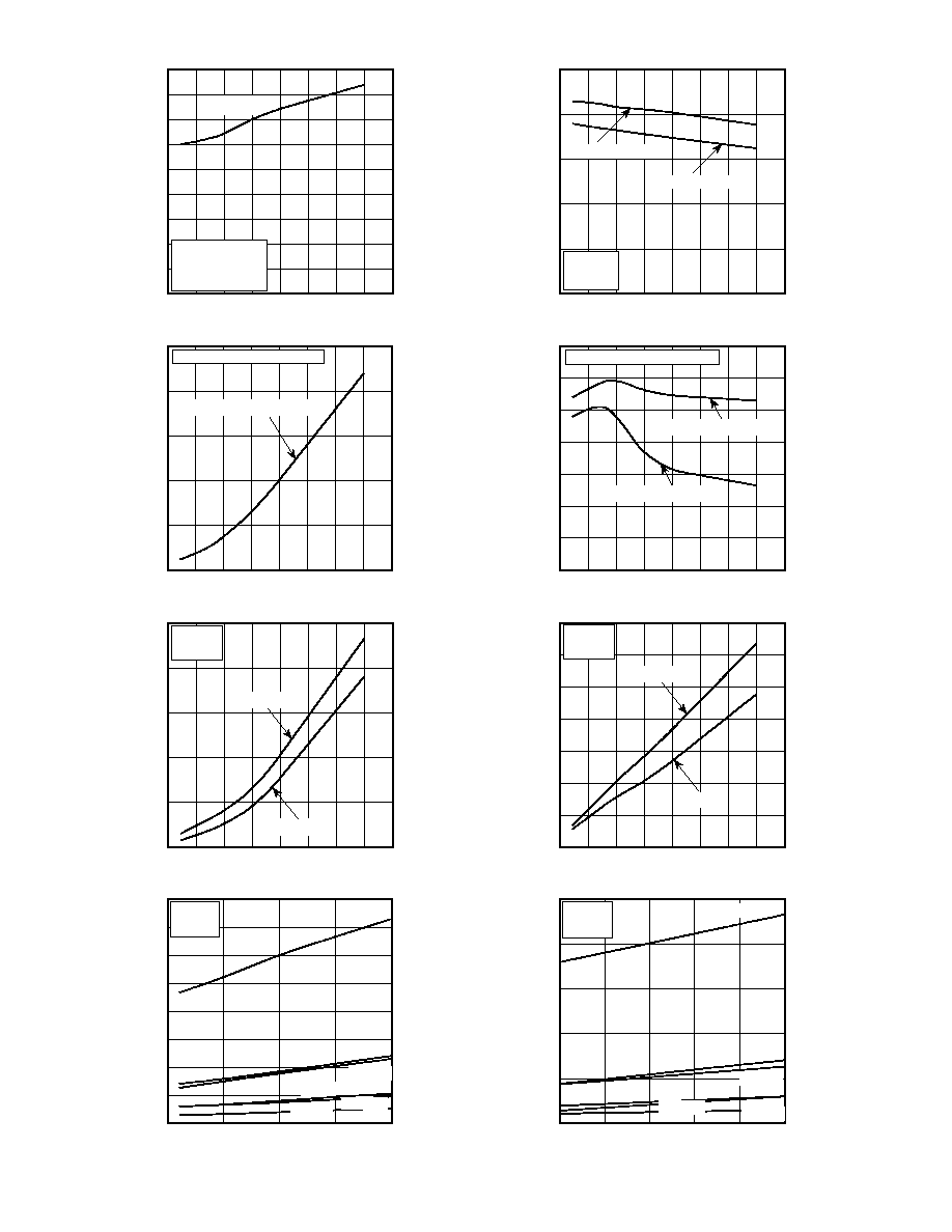
FIGURE 9, Turn-On Delay Time vs Collector Current
FIGURE 10, Turn-Off Delay Time vs Collector Current
I
CE
, COLLECTOR TO EMITTER CURRENT (A)
I
CE
, COLLECTOR TO EMITTER CURRENT (A)
FIGURE 11, Current Rise Time vs Collector Current
FIGURE 12, Current Fall Time vs Collector Current
I
CE
, COLLECTOR TO EMITTER CURRENT (A)
I
CE
, COLLECTOR TO EMITTER CURRENT (A)
FIGURE 13, Turn-On Energy Loss vs Collector Current
FIGURE 14, Turn Off Energy Loss vs Collector Current
R
G
, GATE RESISTANCE (OHMS)
T
J
, JUNCTION TEMPERATURE (∞C)
FIGURE 15, Switching Energy Losses vs. Gate Resistance
FIGURE 16, Switching Energy Losses vs Junction Temperature
R
G
=
1.0, L
=
100
µ
H, V
CE
=
800V
V
CE
= 800V
T
J
= 25∞C
or 125∞C
R
G
= 1.0
L = 100µH
V
GE
= 15V
T
J
=
25 or 125∞C,V
GE
=
15V
10 30 50 70 90 110 130 150 170
10 30 50 70 90 110 130 150 170
10 30
50 70 90 110 130 150 170
10 30 50 70 90 110 130 150 170
10 30 50 70 90 110 130 150 170
10 30 50 70 90 110 130 150 170
0
5
10
15
20
0
25
50
75
100
125
R
G
=
1.0, L
=
100
µ
H, V
CE
=
800V
45
40
35
30
25
20
15
10
5
0
250
200
150
100
50
0
50
40
30
20
10
0
80
70
60
50
40
30
20
10
0
T
J
=
125∞C, V
GE
=
15V
T
J
=
25∞C, V
GE
=
15V
500
400
300
200
100
0
140
120
100
80
60
40
20
0
14
12
10
8
6
4
2
0
50
40
30
20
10
0
V
CE
= 800V
V
GE
= +15V
R
G
= 1.0
T
J
=
125∞C
T
J
=
25∞C
V
CE
= 800V
V
GE
= +15V
R
G
= 1.0
T
J
=
125∞C
T
J
=
25∞C
E
on2,
150A
E
off,
150A
E
on2,
75A
E
off,
75A
E
on2,
37.5A
E
off,
37.5A
V
CE
= 800V
V
GE
= +15V
T
J
= 125∞C
V
CE
= 800V
V
GE
= +15V
R
G
= 1.0
E
on2,
150A
E
off,
150A
E
on2,
75A
E
off,
75A
E
on2,
37.5A
E
off,
37.5A
052-6283 Rev A 3-2006
APT50GF120JRDQ3
TYPICAL PERFORMANCE CURVES
0.25
0.20
0.15
0.10
0.05
0
Z
JC
, THERMAL IMPEDANCE (∞C/W)
0.3
SINGLE PULSE
RECTANGULAR PULSE DURATION (SECONDS)
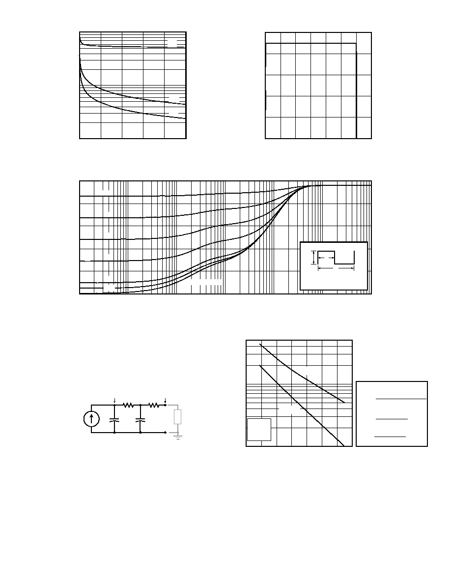
Figure 19a, Maximum Effective Transient Thermal Impedance, Junction-To-Case vs Pulse Duration
10
-5
10
-4
10
-3
10
-2
10
-1
1.0
10
1,000
500
100
50
10
250
200
150
100
50
0
C, CAPACITANCE (
P
F)
I
C
, COLLECTOR CURRENT (A)
V
CE
, COLLECTOR-TO-EMITTER VOLTAGE (VOLTS)
V
CE
, COLLECTOR TO EMITTER VOLTAGE
Figure 17, Capacitance vs Collector-To-Emitter Voltage
Figure 18,Minimim Switching Safe Operating Area
0
10
20
30
40
50
0
200 400 600 800 1000 1200 1400
FIGURE 19b, TRANSIENT THERMAL IMPEDANCE MODEL
10 20
30
40
50
60
70
80
F
MAX
, OPERATING FREQUENCY (kHz)
I
C
, COLLECTOR CURRENT (A)
Figure 20, Operating Frequency vs Collector Current
T
J
= 125
∞
C
D = 50 %
V
CE
= 800V
R
G
= 1.0
50
10
5
1
0.5
0.1
0.05
F
max
=
min (f
max
, f
max2
)
0.05
f
max1
=
t
d(on)
+ t
r
+ t
d(off)
+ t
f
P
diss
- P
cond
E
on2
+ E
off
f
max2
=
P
diss
=
T
J
- T
C
R
JC
C
res
C
ies
C
oes
D = 0.9
0.7
Peak TJ = PDM x ZJC + TC
Duty Factor D =
t1
/
t2
t2
t1
P
DM
Note:
0.655
0.175
0.0307
0.595
Dissipated Power
(Watts)
T
J
(∞C)
T
C
(∞C)
Z
EXT
are the external thermal
impedances: Case to sink,
sink to ambient, etc. Set to
zero when modeling only
the case to junction.
Z
E
X
T
T
C
= 75
∞
C
T
C
= 100
∞
C
052-6283 Rev A 3-2006
APT50GF120JRDQ3
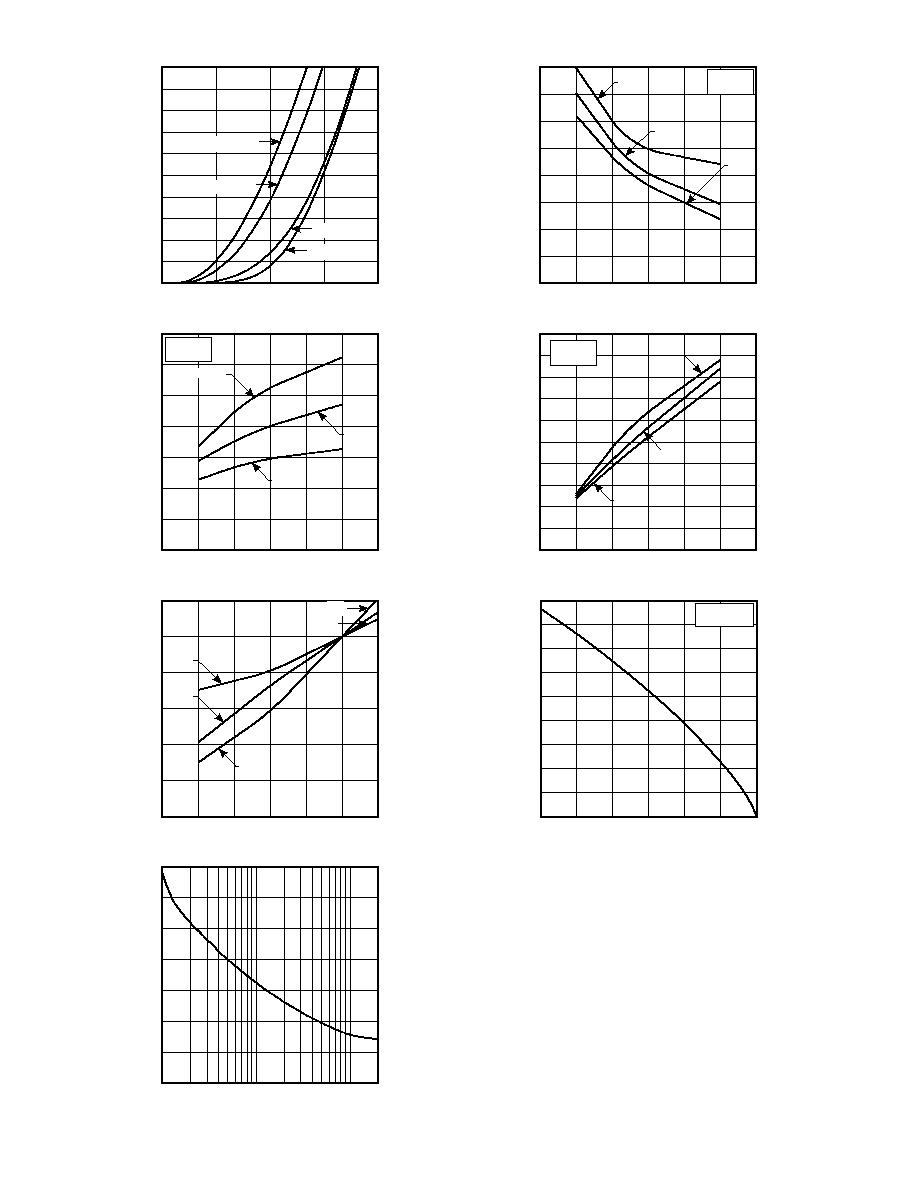
Figure 22, Turn-on Switching Waveforms and Definitions
Figure 23, Turn-off Switching Waveforms and Definitions
T
J
= 125∞C
Switching Energy
5%
10%
t
d(on)
90%
10%
t
r
T
J
= 125∞C
Switching Energy
0
90%
t
d(off)
10%
t
f
90%
APT60DQ120
Collector Current
Collector Voltage
Gate Voltage
Collector Voltage
Collector Current
Gate Voltage
I
C
A
D.U.T.
V
CE
Figure 21, Inductive Switching Test Circuit
V
CC
052-6283 Rev A 3-2006
APT50GF120JRDQ3
TYPICAL PERFORMANCE CURVES
Characteristic / Test Conditions
Maximum Average Forward Current (T
C
= 85∞C, Duty Cycle = 0.5)
RMS Forward Current (Square wave, 50% duty)
Non-Repetitive Forward Surge Current (T
J
= 45∞C, 8.3ms)
Symbol
I
F
(AV)
I
F
(RMS)
I
FSM
Symbol
V
F
Characteristic / Test Conditions
I
F
= 75A
Forward Voltage
I
F
= 150A
I
F
= 75A, T
J
= 125∞C
STATIC ELECTRICAL CHARACTERISTICS
UNIT
Amps
UNIT
Volts
MIN
TYP
MAX
2.8
3.48
2.17
APT50GF120JRDQ3
60
73
540
DYNAMIC CHARACTERISTICS
MAXIMUM RATINGS
All Ratings: T
C
= 25∞C unless otherwise specified.
ULTRAFAST SOFT RECOVERY ANTI-PARALLEL DIODE
MIN
TYP
MAX-
-
60
-
265
-
560
-
5
-
-
350
-
2890
-
13
-
-
150
-
4720
-
-
40
UNIT
ns
nC
Amps
ns
nC
Amps
ns
nC
Amps
Characteristic
Reverse Recovery Time
Reverse Recovery Time
Reverse Recovery Charge
Maximum Reverse Recovery Current
Reverse Recovery Time
Reverse Recovery Charge
Maximum Reverse Recovery Current
Reverse Recovery Time
Reverse Recovery Charge
Maximum Reverse Recovery Current
Symbol
t
rr
t
rr
Q
rr
I
RRM
t
rr
Q
rr
I
RRM
t
rr
Q
rr
I
RRM
Test Conditions
I
F
= 60A, di
F
/dt = -200A/µs
V
R
= 800V, T
C
= 25∞C
I
F
= 60A, di
F
/dt = -200A/µs
V
R
= 800V, T
C
= 125∞C
I
F
= 60A, di
F
/dt = -1000A/µs
V
R
= 800V, T
C
= 125∞C
I
F
= 1A, di
F
/dt = -100A/µs, V
R
= 30V, T
J
= 25∞C
FIGURE 24b, TRANSIENT THERMAL IMPEDANCE MODEL
Z
JC
, THERMAL IMPEDANCE (∞C/W)
10
-5
10
-4
10
-3
10
-2
10
-1
1.0
RECTANGULAR PULSE DURATION (seconds)
FIGURE 24a. MAXIMUM EFFECTIVE TRANSIENT THERMAL IMPEDANCE, JUNCTION-TO-CASE vs. PULSE DURATION
0.60
0.50
0.40
0.30
0.20
0.10
0
0.5
SINGLE PULSE
0.1
0.3
0.7
D = 0.9
0.05
Peak TJ = PDM x ZJC + TC
Duty Factor D =
t1
/
t2
t2
t1
P
DM
Note:
0.149
0.238
0.174
0.006
0.091
0.524
Dissipated Power
(Watts)
T
J
(∞C)
T
C
(∞C)
Z
EXT
are the external thermal
impedances: Case to sink,
sink to ambient, etc. Set to
zero when modeling only
the case to junction.
Z
E
X
T
052-6283 Rev A 3-2006
APT50GF120JRDQ3
400
350
300
250
200
150
100
50
0
50
45
40
35
30
25
20
15
10
5
0
Duty cycle = 0.5
T
J
= 175∞C
90
80
70
60
50
40
30
20
10
0
T
J
, JUNCTION TEMPERATURE (∞C)
Case Temperature (∞C)
Figure 29. Dynamic Parameters vs. Junction Temperature
Figure 30. Maximum Average Forward Current vs. CaseTemperature
V
R
, REVERSE VOLTAGE (V)
Figure 31. Junction Capacitance vs. Reverse Voltage
200
180
160
140
120
100
80
60
40
20
0
7000
6000
5000
4000
3000
2000
1000
0
Q
rr
, REVERSE RECOVERY CHARGE
I
F
,
FORWARD CURRENT
(nC)
(A)
I
RRM
, REVERSE RECOVERY CURRENT
t
rr
, REVERSE RECOVERY TIME
(A)
(ns)
T
J
= 125∞C
V
R
= 800V
T
J
= 125∞C
V
R
= 800V
T
J
= 125∞C
V
R
= 800V
T
J
= 175∞C
T
J
= -55∞C
T
J
= 25∞C
T
J
= 125∞C
0
1
2
3
4
0
200
400
600
800 1000 1200
0
200
400
600
800 1000 1200
0
200
400
600
800 1000 1200
30A
60A
120A
120A
30A
60A
t
rr
Q
rr
Q
rr
t
rr
I
RRM
1.2
1.0
0.8
0.6
0.4
0.2
0.0
350
300
250
200
150
100
50
0
C
J
, JUNCTION CAPACITANCE
K
f
, DYNAMIC PARAMETE
RS
(pF)
(Normalized to 1000A/
µ
s)
I
F(AV)
(A)
0
25
50
75
100
125
150
25
50
75
100
125
150
175
1
10
100 200
120A
60A
30A
V
F
, ANODE-TO-CATHODE VOLTAGE (V)
-di
F
/dt, CURRENT RATE OF CHANGE(A/µs)
Figure 25. Forward Current vs. Forward Voltage
Figure 26. Reverse Recovery Time vs. Current Rate of Change
-di
F
/dt, CURRENT RATE OF CHANGE (A/µs)
-di
F
/dt, CURRENT RATE OF CHANGE (A/µs)
Figure 27. Reverse Recovery Charge vs. Current Rate of Change
Figure 28. Reverse Recovery Current vs. Current Rate of Change
052-6283 Rev A 3-2006
APT50GF120JRDQ3
TYPICAL PERFORMANCE CURVES
4
3
1
2
5
5
Zero
1
2
3
4
di
F
/dt - Rate of Diode Current Change Through Zero Crossing.
I
F
- Forward Conduction Current
I
RRM
- Maximum Reverse Recovery Current.
trr - Reverse
R
ecovery Time, measured from zero crossing where
diode
Qrr - Area Under the Curve Defined by I
RRM
and trr.
current goes from positive to negative, to the point at which the straight
line through I
RRM
and 0.25 I
RRM
passes through zero.
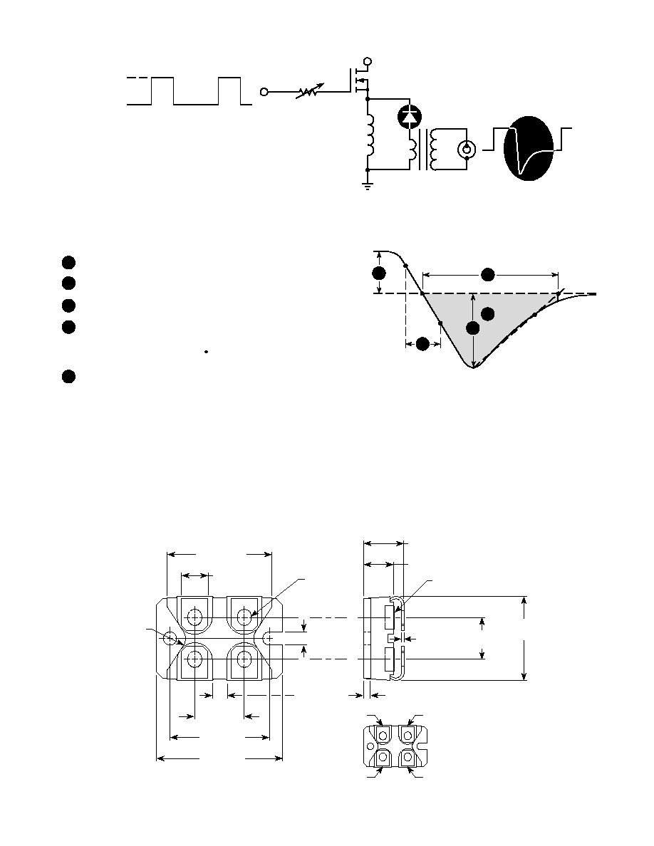
Figure 32. Diode Test Circuit
Figure 33, Diode Reverse Recovery Waveform and Definitions
0.25 IRRM
PEARSON 2878
CURRENT
TRANSFORMER
di
F
/dt Adjust
30µH
D.U.T.
+18V
0V
Vr
trr/Qrr
Waveform
APT10035LLL
SOT-227 (ISOTOP
Æ
) Package Outline
APT's products are covered by one or more of U.S.patents 4,895,810 5,045,903 5,089,434 5,182,234 5,019,522
5,262,336 6,503,786 5,256,583 4,748,103 5,283,202 5,231,474 5,434,095 5,528,058 and foreign patents. US and Foreign patents pending. All Rights Reserved.
ISOTOP
Æ
is a Registered Trademark of SGS Thomson.
31.5 (1.240)
31.7 (1.248)
Dimensions in Millimeters and (Inches)
7.8 (.307)
8.2 (.322)
30.1 (1.185)
30.3 (1.193)
38.0 (1.496)
38.2 (1.504)
14.9 (.587)
15.1 (.594)
11.8 (.463)
12.2 (.480)
8.9 (.350)
9.6 (.378)
Hex Nut M4
(4 places)
0.75 (.030)
0.85 (.033)
12.6 (.496)
12.8 (.504)
25.2 (0.992)
25.4 (1.000)
1.95 (.077)
2.14 (.084)
* Emitter/Anode
Collector/Cathode
Gate
*
r = 4.0 (.157)
(2 places)
4.0 (.157)
4.2 (.165)
(2 places)
W=4.1 (.161)
W=4.3 (.169)
H=4.8 (.187)
H=4.9 (.193)
(4 places)
3.3 (.129)
3.6 (.143)
* Emitter/Anode
Emitter/Anode terminals are
shorted internally. Current
handling capability is equal
for either Emitter/Anode terminal.