PRELIMINAR
Y
APT50GF60B2RD/LRD
600
600
±
20
80
50
160
100
300
-55 to 150
300
G
C
E
MAXIMUM RATINGS (IGBT)
All Ratings: T
C
= 25
∞
C unless otherwise specified.
052-6253 Rev A
The Fast IGBT
TM
is a new generation of high voltage power IGBTs. Using Non-
Punch Through Technology the Fast IGBTTM combined with an APT free-
wheeling ultraFast Recovery Epitaxial Diode (FRED) offers superior
ruggedness and fast switching speed.
∑ Low Forward Voltage Drop
∑ High Freq. Switching to 20KHz
∑ Low Tail Current
∑ Ultra Low Leakage Current
∑ RBSOA and SCSOA Rated
∑ Ultrafast Soft Recovery Antiparallel Diode
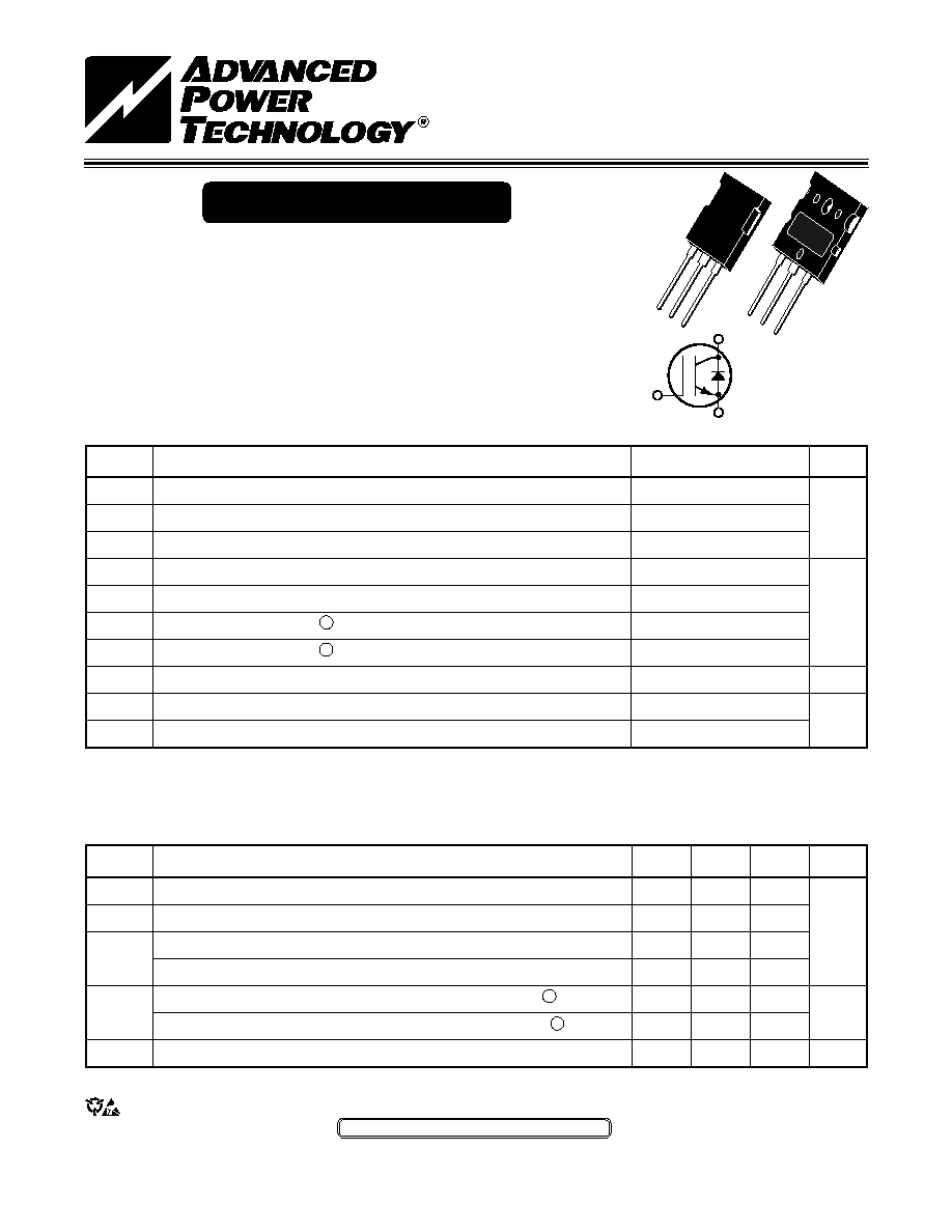
Fast IGBT
& FRED
TO-264
(LRD)
G
C
E
T-Max
TM
(B2RD)
G
C
E
APT50GF60B2RD
APT50GF60LRD
600V
80A
APT50GF60B2RD
APT50GF60LRD
MIN
TYP
MAX
600
4.5
5.5
6.5
2.1
2.7
2.2
2.8
0.50
TBD
±
100
Characteristic / Test Conditions
Collector-Emitter Breakdown Voltage (V
GE
= 0V, I
C
= 0.50mA)
Gate Threshold Voltage (V
CE
= V
GE
, I
C
= 700
µ
A, T
j
= 25
∞
C)
Collector-Emitter On Voltage (V
GE
= 15V, I
C
= I
C2
, T
j
= 25
∞
C)
Collector-Emitter On Voltage (V
GE
= 15V, I
C
= I
C2
, T
j
= 125
∞
C)
Collector Cut-off Current (V
CE
= V
CES
, V
GE
= 0V, T
j
= 25
∞
C)
2
Collector Cut-off Current (V
CE
= V
CES
, V
GE
= 0V, T
j
= 125
∞
C)
2
Gate-Emitter Leakage Current (V
GE
=
±
20V, V
CE
= 0V)
Symbol
BV
CES
V
GE
(TH)
V
CE
(ON)
I
CES
I
GES
STATIC ELECTRICAL CHARACTERISTICS (IGBT)
UNIT
Volts
mA
nA
Symbol
V
CES
V
CGR
V
GE
I
C1
I
C2
I
CM1
I
CM2
P
D
T
J
,T
STG
T
L
Parameter
Collector-Emitter Voltage
Collector-Gate Voltage (R
GE
= 20K
)
Gate-Emitter Voltage
Continuous Collector Current @ T
C
= 25
∞
C
Continuous Collector Current @ T
C
= 90
∞
C
Pulsed Collector Current
1
@ T
C
= 25
∞
C
Pulsed Collector Current
1
@ T
C
= 90
∞
C
Total Power Dissipation
Operating and Storage Junction Temperature Range
Max. Lead Temp. for Soldering: 0.063" from Case for 10 Sec.
UNIT
Volts
Amps
Watts
∞
C
CAUTION: These Devices are Sensitive to Electrostatic Discharge. Proper Handling Procedures Should Be Followed.
USA
405 S.W. Columbia Street
Bend, Oregon 97702 -1035
Phone: (541) 382-8028
FAX: (541) 388-0364
EUROPE
Avenue J.F. Kennedy B‚t B4 Parc CadÈra Nord
F-33700 Merignac - France
Phone: (33) 5 57 92 15 15
FAX: (33) 5 56 47 97 61
APT Website - http://www.advancedpower.com
052-6253 Rev A
PRELIMINAR
Y
Symbol
C
ies
C
oes
C
res
Q
g
Q
ge
Q
gc
t
d
(on)
t
r
t
d
(off)
t
f
t
d
(on)
t
r
t
d
(off)
t
f
E
on
E
off
E
ts
t
d
(on)
t
r
t
d
(off)
t
f
E
ts
gfe
DYNAMIC CHARACTERISTICS (IGBT)
APT50GF60B2RD/LRD
UNIT
∞
C/W
oz
gm
lb∑in
N∑m
MIN
TYP
MAX
0.42
0.66
40
0.22
6.1
10
1.1
Characteristic
Junction to Case (IGBT)
Junction to Case (FRED)
Junction to Ambient
Package Weight
Mounting Torque using a 6-32 or 3mm Binding Head Machine Screw
Symbol
R
JC
R
JA
W
T
Torque
THERMAL AND MECHANICAL CHARACTERISTICS (IGBT and FRED)
Test Conditions
Capacitance
V
GE
= 0V
V
CE
= 25V
f = 1 MHz
Gate Charge
V
GE
= 15V
V
CC
= 0.5V
CES
I
C
= I
C2
Resistive Switching (25
∞
C)
V
GE
= 15V
V
CC
= .8V
CES
I
C
= I
C2
R
G
= 10
Inductive Switching (150
∞
C)
V
CLAMP
(Peak)
= 0.66V
CES
V
GE
= 15V
I
C
= I
C2
R
G
= 10
T
J
= +150
∞
C
Inductive Switching (25
∞
C)
V
CLAMP
(Peak)
= 0.66V
CES
V
GE
= 15V
I
C
= I
C2
R
G
= 10
T
J
= +25
∞
C
V
CE
= 20V, I
C
= I
C2
MIN
TYP
MAX
2600
3600
475
710
165
250
170
225
25
45
100
140
20
100
160
200
30
50
90
135
290
435
170
340
2.2
2.4
4.6
30
90
260
100
4.3
6
UNIT
pF
nC
ns
ns
mJ
ns
mJ
S
Characteristic
Input Capacitance
Output Capacitance
Reverse Transfer Capacitance
Total Gate Charge
3
Gate-Emitter Charge
Gate-Collector ("Miller ") Charge
Turn-on Delay Time
Rise Time
Turn-off Delay Time
Fall Time
Turn-on Delay Time
Rise Time
Turn-off Delay Time
Fall Time
Turn-on Switching Energy
4
Turn-off Switching Energy
Total Switching Losses
4
Turn-on Delay Time
Rise Time
Turn-off Delay Time
Fall Time
Total Switching Losses
4
Forward Transconductance
1
Repetitive Rating: Pulse width limited by maximum junction temperature.
2
Leakages include the FRED and IGBT.
3
See MIL-STD-750 Method 3471
4
Switching losses include the FRED and IGBT.
APT Reserves the right to change, without notice, the specifications and information contained herein.
052-6253 Rev A
EUROPE
Avenue J.F. Kennedy B‚t B4 Parc CadÈra Nord
F-33700 Merignac - France
Phone: (33) 5 57 92 15 15
FAX: (33) 5 56 47 97 61
USA
405 S.W. Columbia Street
Bend, Oregon 97702 -1035
Phone: (541) 382-8028
FAX: (541) 388-0364
APT50GF60B2RD/LRD
PRELIMINARY
Power dissipation
P
tot
=
(
T
C
)
parameter:
T
j
150 ∞C
0
20
40
60
80
100
120
∞C
160
T
C
0
40
80
120
160
200
240
W
320
P
tot
Collector current
I
C
=
(
T
C
)
parameter:
V
GE
15 V ,
T
j
150 ∞C
0
20
40
60
80
100
120
∞C
160
T
C
0
10
20
30
40
50
60
A
80
I
C
Safe operating area
I
C
=
(
V
CE
)
parameter:
D
= 0
, T
C
= 25∞C ,
T
j
150 ∞C
-1
10
0
10
1
10
2
10
3
10
A
I
C
10
0
10
1
10
2
10
3
V
V
CE
DC
10 ms
1 ms
100 µs
10 µs
t
p
= 2.9µs
Transient thermal impedance IGBT
Z
th JC
=
(
t
p
)
parameter:
D = t
p
/
T
-3
10
-2
10
-1
10
0
10
K/W
Z
thJC
10
-5
10
-4
10
-3
10
-2
10
-1
10
0
s
t
p
single pulse
0.01
0.02
0.05
0.10
0.20
D = 0.50
052-6253 Rev A
EUROPE
Avenue J.F. Kennedy B‚t B4 Parc CadÈra Nord
F-33700 Merignac - France
Phone: (33) 5 57 92 15 15
FAX: (33) 5 56 47 97 61
USA
405 S.W. Columbia Street
Bend, Oregon 97702 -1035
Phone: (541) 382-8028
FAX: (541) 388-0364
APT50GF60B2RD/LRD
PRELIMINARY
Typ. output characteristics
I
C
=
f
(
V
CE
)
parameter:
t
p
= 80 µs,
T
j
= 25 ∞C
0
1
2
3
V
5
V
CE
0
10
20
30
40
50
60
70
80
A
100
I
C
17V
15V
13V
11V
9V
7V
Typ. output characteristics
I
C
=
f
(
V
CE
)
parameter:
t
p
= 80 µs,
T
j
= 125 ∞C
0
1
2
3
V
5
V
CE
0
10
20
30
40
50
60
70
80
A
100
I
C
17V
15V
13V
11V
9V
7V
Short circuit safe operating area
I
Csc
=
f
(
V
CE
) ,
T
j
= 150∞C
parameter:
V
GE
= ± 15 V,
t
sc
10 µs, L < 50 nH
0
100
200
300
400
500
600
V
800
V
CE
0
2
4
6
10
I
Csc
/
I
C(90∞C)
Reverse biased safe operating area
I
Cpuls
=
f
(V
CE
) ,
T
j
= 150∞C
parameter:
V
GE
= 15 V
0
100
200
300
400
500
600
V
800
V
CE
0.0
0.5
1.0
1.5
2.5
I
Cpuls
/
I
C
I
Cpulse
/I
C1
I
Csc
/I
C2

052-6253 Rev A
APT50GF60B2RD/LRD
PRELIMINAR
Y
Characteristic / Test Conditions
Maximum D.C. Reverse Voltage
Maximum Peak Repetitive Reverse Voltage
Maximum Working Peak Reverse Voltage
Maximum Average Forward Current (T
C
= 85
∞
C, Duty Cycle = 0.5)
RMS Forward Current
Non-Repetitive Forward Surge Current (T
J
= 45
∞
C, 8.3ms)
Symbol
V
R
V
RRM
V
RWM
I
F
(AV)
I
F
(RMS)
I
FSM
Symbol
V
F
Characteristic / Test Conditions
I
F
= 60A
Maximum Forward Voltage
I
F
= 120A
I
F
= 60A, T
J
= 150
∞
C
STATIC ELECTRICAL CHARACTERISTICS (FRED)
UNIT
Volts
Amps
UNIT
Volts
MIN
TYP
MAX
1.8
1.75
1.5
APT50GF60B2RD/LRD
600
60
100
600
MAXIMUM RATINGS (FRED)
All Ratings: T
C
= 25
∞
C unless otherwise specified.
ULTRAFAST SOFT RECOVERY PARALLEL DIODE
MIN
TYP
MAX
55
70
70
90
160
160
10
17
20
30
350
900
6
6
800
500
UNIT
ns
Amps
nC
Volts
A/
µ
s
Characteristic
Reverse Recovery Time, I
F
= 1.0A, di
F
/dt
= -15A/
µ
s, V
R
= 30V,
T
J
= 25
∞
C
Reverse Recovery Time
T
J
= 25
∞
C
I
F
= 60A, di
F
/dt
= -480A/
µ
s, V
R
= 350V
T
J
= 100
∞
C
Forward Recovery Time
T
J
= 25
∞
C
I
F
= 60A, di
F
/dt
= 480A/
µ
s, V
R
= 350V
T
J
= 100
∞
C
Reverse Recovery Current
T
J
= 25
∞
C
I
F
= 60A, di
F
/dt
= -480A/
µ
s, V
R
= 350V
T
J
= 100
∞
C
Recovery Charge
T
J
= 25
∞
C
I
F
= 60A, di
F
/dt
= -480A/
µ
s, V
R
= 350V
T
J
= 100
∞
C
Forward Recovery Voltage
T
J
= 25
∞
C
I
F
= 60A, di
F
/dt
= 480A/
µ
s, V
R
= 350V
T
J
= 100
∞
C
Rate of Fall of Recovery Current
T
J
= 25
∞
C
I
F
= 60A, di
F
/dt
= -480A/
µ
s, V
R
= 350V
T
J
= 100
∞
C
DYNAMIC CHARACTERISTICS (FRED)
Symbol
t
rr1
t
rr2
t
rr3
t
fr1
t
fr2
I
RRM1
I
RRM2
Q
rr1
Q
rr2
V
fr1
V
fr2
diM/dt
PRELIMINAR
Y
Z
JC
, THERMAL IMPEDANCE
t
rr
, REVERSE RECOVERY TIME
I
RRM
, REVERSE RECOVERY CURRENT
I
F
, FORWARD CURRENT
(
∞
C/W)
(nano-SECONDS)
(AMPERES)
(AMPERES)
t
fr
, FORWARD RECOVERY TIME
K
f
, DYNAMIC PARAMETERS
Q
rr
, REVERSE RECOVERY CHARGE
(nano-SECONDS)
(NORMALIZED)
(nano-COULOMBS)
V
fr
, FORWARD RECOVERY VOLTAGE
(VOLTS)
V
F
, ANODE-TO-CATHODE VOLTAGE (VOLTS)
di
F
/dt, CURRENT SLEW RATE (AMPERES/
µ
SEC)
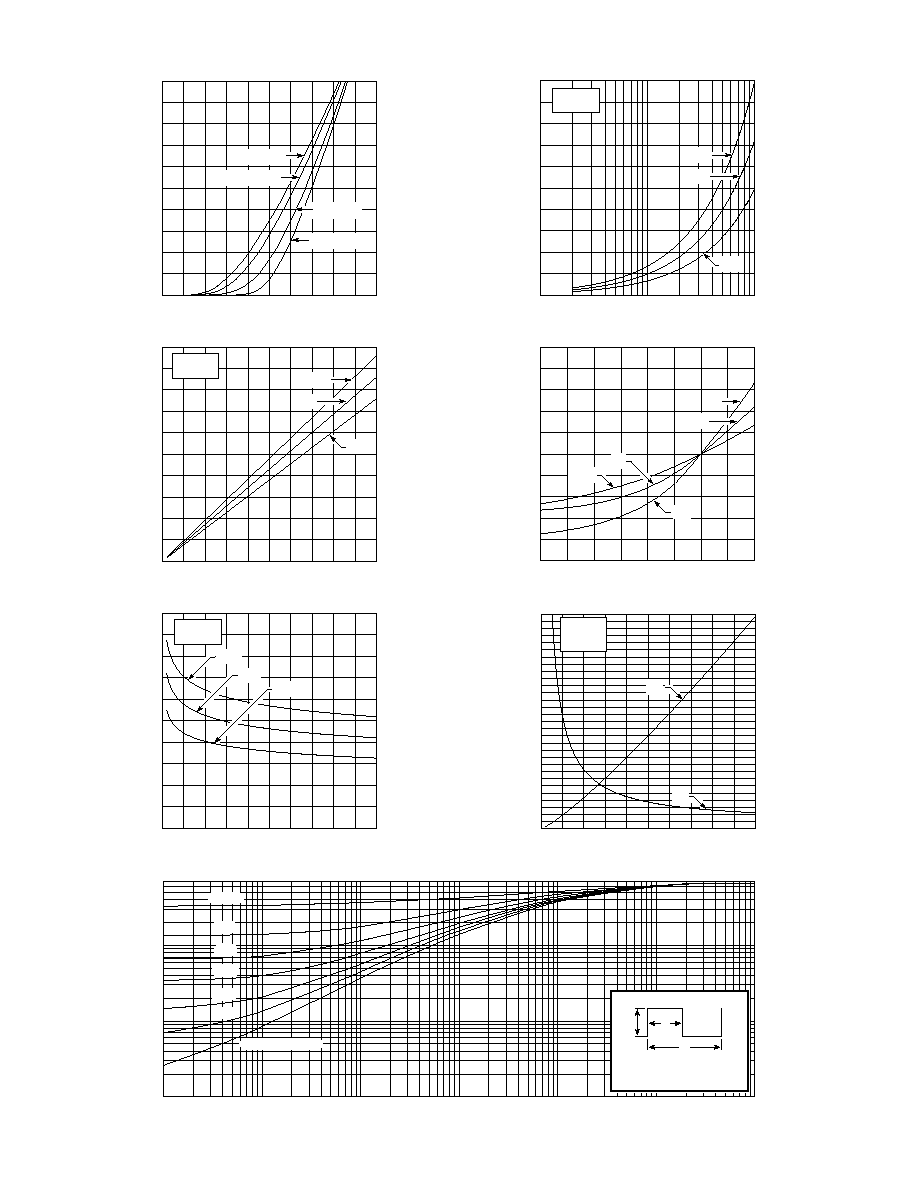
Figure 1, Forward Voltage Drop vs Forward Current
Figure 2, Reverse Recovery Charge vs Current Slew Rate
di
F
/dt, CURRENT SLEW RATE (AMPERES/
µ
SEC)
T
J
, JUNCTION TEMPERATURE (
∞
C)
Figure 3, Reverse Recovery Current vs Current Slew Rate
Figure 4, Dynamic Parameters vs Junction Temperature
di
F
/dt, CURRENT SLEW RATE (AMPERES/
µ
SEC)
di
F
/dt, CURRENT SLEW RATE (AMPERES/
µ
SEC)
Figure 5, Reverse Recovery Time vs Current Slew Rate
Figure 6, Forward Recovery Voltage/Time vs Current Slew Rate
V
R
, REVERSE VOLTAGE (VOLTS)
Figure 7, Maximum Effective Transient Thermal Impedance, Junction-To-Case vs Pulse Duration
APT50GF60B2RD/LRD
052-6253 Rev A
0
0.5
1.0
1.5
2.0
2.5
10
50
100
500
1000
0
200
400
600
800
1000
-50
-25
0
25
50
75
100 125
150
0
200
400
600
800
1000
0
200
400
600
800
1000
10
-5
10
-4
10
-3
10
-2
10
-1
1.0
10
RECTANGULAR PULSE DURATION (SECONDS)
TJ = 100
∞
C
VR = 350V
TJ = 100
∞
C
VR = 350V
TJ = 100
∞
C
VR = 350V
TJ = 100
∞
C
VR = 350V
IF = 60A
T
J
= 150
∞
C
T
J
= -55
∞
C
T
J
= 100
∞
C
120A
30A
V
fr
T
fr
t
rr
Q
rr
Q
rr
t
rr
200
160
120
80
40
0
50
40
30
20
10
0
200
160
120
80
40
0
0.7
0.5
0.1
0.05
0.01
0.005
0.001
2500
2000
1500
1000
500
0
2.0
1.6
1.2
0.8
0.4
0.0
1200
1000
800
600
400
200
0
120A
60A
30A
120A
I
RRM
60A
15.0
12.5
10.0
7.5
5.0
2.5
0
T
J
= 25
∞
C
60A
30A
Note:
Duty Factor D =
t1/t
2
Peak TJ = PDM x Z
JC + TC
t1
t2
P
DM
0.1
SINGLE PULSE
0.02
0.05
0.2
D=0.5
0.01
PRELIMINAR
Y
PRELIMINAR
Y
APT50GF60B2RD/LRD
052-6253 Rev A
PEARSON 411
CURRENT
TRANSFORMER
0.5 IRRM
di
F
/dt Adjust
30
µ
H
D.U.T.
+15v
-15v
0v
Vr
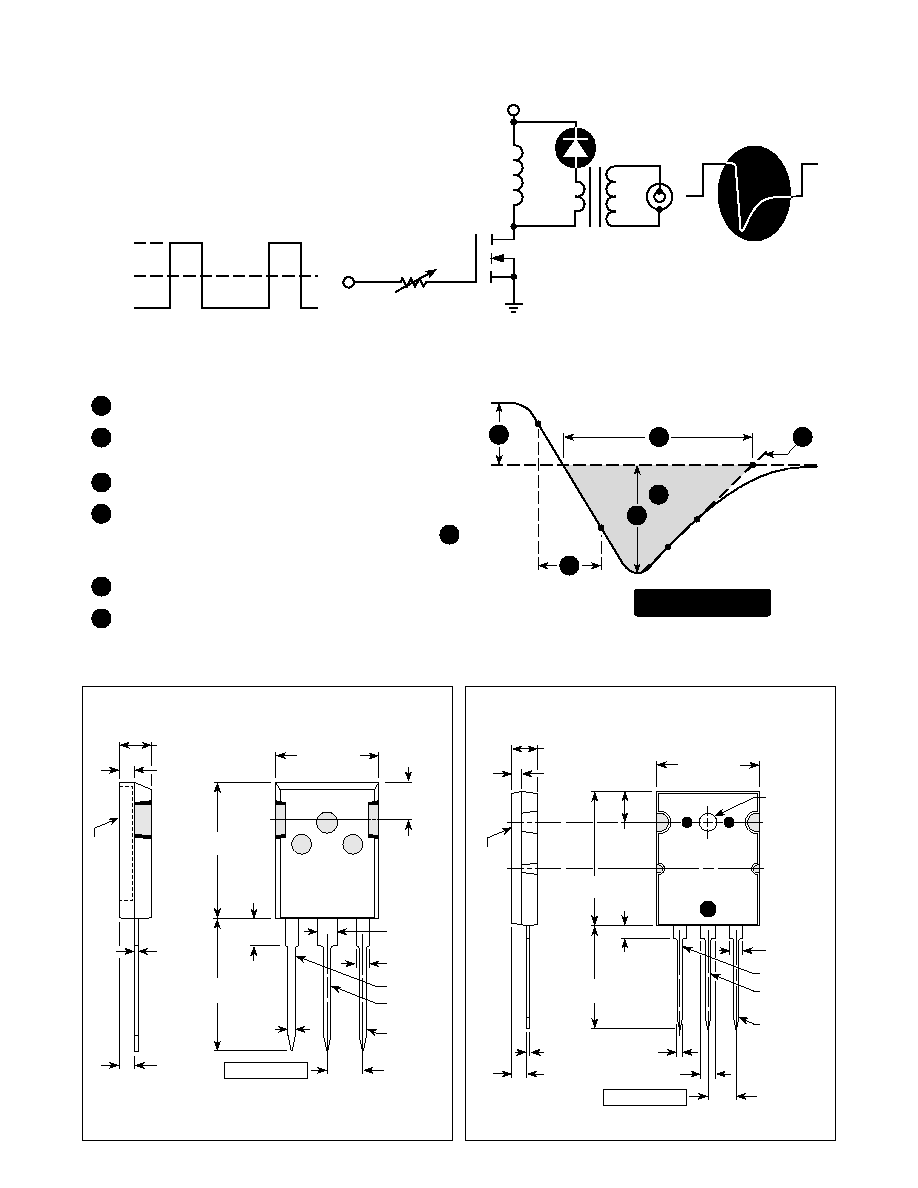
Dimensions in Millimeters and (Inches)
Dimensions in Millimeters and (Inches)
4
3
1
2
5
5
0.75 IRRM
trr/Qrr
Waveform
Zero
6
1
2
3
4
6
di
F
/dt - Current Slew Rate, Rate of Forward
Current Change Through Zero Crossing.
I
F
- Forward Conduction Current
I
RRM
- Peak Reverse Recovery Current.
trr - Reverse Recovery Time Measured from Point of I
F
Qrr - Area Under the Curve Defined by I
RRM
and trr.
diM/dt - Maximum Rate of Current Change During the Trailing Portion of trr.
Current Falling Through Zero to a Tangent Line
{
diM/dt
}
Extrapolated Through Zero Defined by 0.75 and 0.50 I
RRM
.
6
Figure 25, Diode Reverse Recovery Test Circuit and Waveforms
Figure 8, Diode Reverse Recovery Waveform and Definitions
Qrr = 1/2
(
trr . I
RRM
)
4.69 (.185)
5.31 (.209)
1.49 (.059)
2.49 (.098)
2.21 (.087)
2.59 (.102)
0.40 (.016)
0.79 (.031)
Collector
(Cathode)
Emitter
(Anode)
Gate
Collector
(Cathode)
Emitter
(Anode)
Gate
Collector
(Cathode)
Collector
(Cathode)
19.51 (.768)
20.50 (.807)
19.81 (.780)
21.39 (.842)
25.48 (1.003)
26.49 (1.043)
2.29 (.090)
2.69 (.106)
0.76 (.030)
1.30 (.051)
3.10 (.122)
3.48 (.137)
4.60 (.181)
5.21 (.205)
1.80 (.071)
2.01 (.079)
2.59 (.102)
3.00 (.118)
0.48 (.019)
0.84 (.033)
2.29 (.090)
2.69 (.106)
5.79 (.228)
6.20 (.244)
2.79 (.110)
3.18 (.125)
5.45 (.215) BSC
2-Plcs.
15.49 (.610)
16.26 (.640)
5.38 (.212)
6.20 (.244)
4.50
(.177) Max.
19.81 (.780)
20.32 (.800)
20.80 (.819)
21.46 (.845)
1.65 (.065)
2.13 (.084)
1.01 (.040)
1.40 (.055)
5.45 (.215) BSC
2.87 (.113)
3.12 (.123)
2-Plcs.
TO-264 Package Outline
T-MAXTM Package Outline