APT50M75JLLU3
A
P
T
5
0M
75J
L
L
U
3 ≠ R
e
v 0
A
p
r
i
l
,
2004
APT website ≠ http://www.advancedpower.com
1 ≠ 8
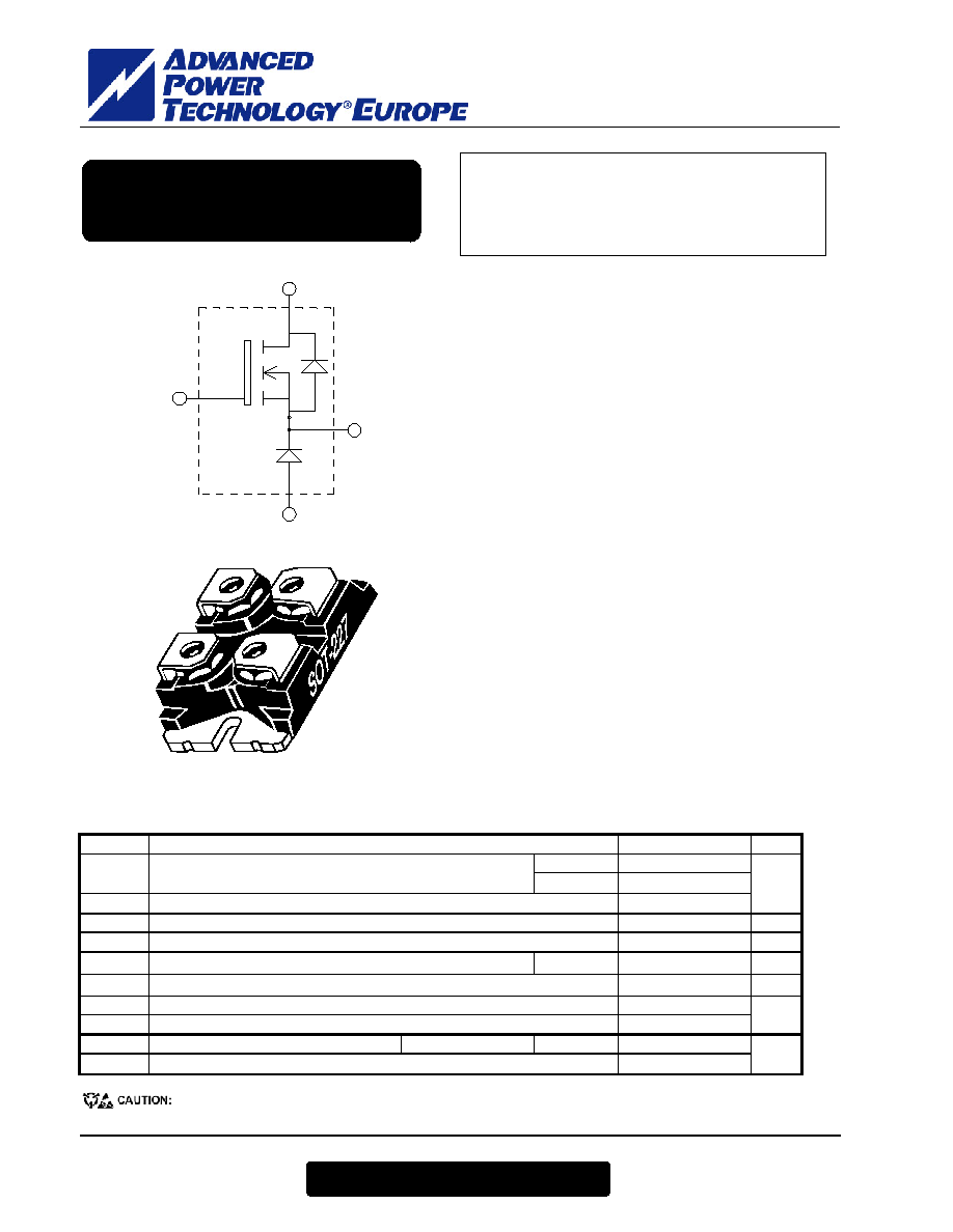
ISOTOP
“
Absolute maximum ratings
These Devices are sensitive to Electrostatic Discharge. Proper Handing Procedures Should Be Followed.
A
S
G
D
Symbol Parameter
Max
ratings
Unit
V
DSS
Drain - Source Breakdown Voltage
500
V
T
c
= 25∞C
51
I
D
Continuous Drain Current
T
c
= 80∞C
39
I
DM
Pulsed Drain current
204
A
V
GS
Gate - Source Voltage
±30
V
R
DSon
Drain - Source ON Resistance
75
m
W
P
D
Maximum Power Dissipation
T
c
= 25∞C
290
W
I
AR
Avalanche current (repetitive and non repetitive)
51
A
E
AR
Repetitive Avalanche Energy
50
E
AS
Single Pulse Avalanche Energy
2500
mJ
IF
AV
Maximum Average Forward Current
Duty cycle=0.5
Tc = 80∞C
30
IF
RMS
RMS Forward Current (Square wave, 50% duty)
39
A
V
DSS
= 500V
R
DSon
= 75m
W max @ Tj = 25∞C
I
D
= 51A @ Tc = 25∞C
Application
∑ AC and DC motor control
∑ Switched Mode Power Supplies
Features
∑ Power MOS 7
Æ
MOSFETs
- Low
R
DSon
- Low input and Miller capacitance
- Low gate charge
- Fast intrinsic reverse diode
- Avalanche energy rated
- Very
rugged
∑ ISOTOP
Æ
Package (SOT-227)
∑ Very low stray inductance
∑ High level of integration
Benefits
∑ Outstanding performance at high frequency operation
∑ Direct mounting to heatsink (isolated package)
∑ Low junction to case thermal resistance
∑ Very rugged
∑ Low profile
ISOTOP
Æ
Buck chopper
MOSFET Power Module
A
D
G
S

APT50M75JLLU3
A
P
T
5
0M
75J
L
L
U
3 ≠ R
e
v 0
A
p
r
i
l
,
2004
APT website ≠ http://www.advancedpower.com
2 ≠ 8
All ratings @ T
j
= 25∞C unless otherwise specified
Electrical Characteristics
Symbol Characteristic
Test
Conditions
Min Typ Max Unit
BV
DSS
Drain - Source Breakdown Voltage V
GS
= 0V, I
D
= 250µA
500
V
V
GS
= 0V,V
DS
= 500V
T
j
= 25∞C
100
I
DSS
Zero Gate Voltage Drain Current
V
GS
= 0V,V
DS
= 400V
T
j
= 125∞C
500
µA
R
DS(on)
Drain ≠ Source on Resistance
V
GS
= 10V, I
D
= 25.5A
75
m
W
V
GS(th)
Gate Threshold Voltage
V
GS
= V
DS
, I
D
= 1mA
3
5
V
I
GSS
Gate ≠ Source Leakage Current
V
GS
= ±20
V, V
DS
= 0V
±100
nA
Dynamic Characteristics
Symbol Characteristic
Test
Conditions
Min Typ Max Unit
C
iss
Input
Capacitance
5590
C
oss
Output
Capacitance
1180
C
rss
Reverse Transfer Capacitance
V
GS
= 0V
V
DS
= 25V
f = 1MHz
85
pF
Q
g
Total gate Charge
123
Q
gs
Gate ≠ Source Charge
33
Q
gd
Gate ≠ Drain Charge
V
GS
= 10V
V
Bus
= 250V
I
D
= 51A
65
nC
T
d(on)
Turn-on Delay Time
10
T
r
Rise Time
20
T
d(off)
Turn-off Delay Time
21
T
f
Fall Time
Resistive Switching
V
GS
= 15V
V
Bus
= 250V
I
D
= 51A
R
G
= 0.6
W
5
ns
Eon
Turn-on Switching Energy
u
755
Eoff
Turn-off Switching Energy
v
Inductive switching @ 25∞C
V
GS
= 15V, V
Bus
= 330V
I
D
= 51A,
R
G
= 5
726
µJ
Eon
Turn-on Switching Energy
u
1241
Eoff
Turn-off Switching Energy
v
Inductive switching @ 125∞C
V
GS
= 15V, V
Bus
= 330V
I
D
= 51A,
R
G
= 5
846
µJ
u Eon includes diode reverse recovery
v In accordance with JEDEC standard JESD24-1.
APT50M75JLLU3
A
P
T
5
0M
75J
L
L
U
3 ≠ R
e
v 0
A
p
r
i
l
,
2004
APT website ≠ http://www.advancedpower.com
3 ≠ 8
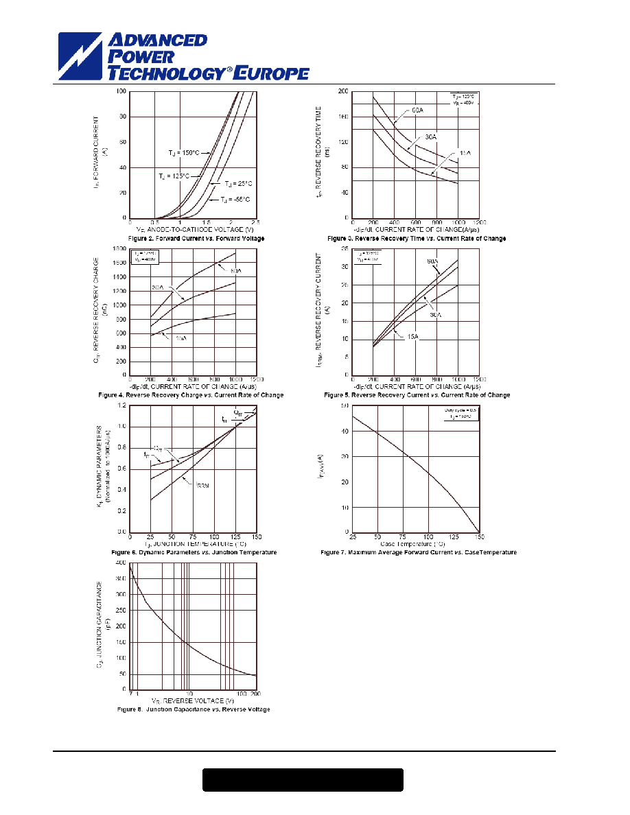
Diode ratings and characteristics
Symbol Characteristic
Test
Conditions
Min Typ Max Unit
I
F
= 30A
1.6
1.8
I
F
= 60A
1.9
V
F
Diode Forward Voltage
I
F
= 30A
T
j
= 125∞C
1.4
V
V
R
= 600V
T
j
= 25∞C
250
I
RM
Maximum Reverse Leakage Current
V
R
= 600V
T
j
= 125∞C
500
µA
C
T
Junction
Capacitance
V
R
=
200V
44 pF
Reverse Recovery Time
I
F
=1A,V
R
=30V
di/dt =100A/µs
T
j
= 25∞C
23
T
j
= 25∞C
85
t
rr
Reverse Recovery Time
T
j
= 125∞C
160
ns
T
j
= 25∞C
4
I
RRM
Maximum Reverse Recovery Current
T
j
= 125∞C
8
A
T
j
= 25∞C
130
Q
rr
Reverse Recovery Charge
I
F
= 30A
V
R
= 400V
di/dt =200A/µs
T
j
= 125∞C
700
nC
t
rr
Reverse Recovery Time
70
ns
Q
rr
Reverse Recovery Charge
1300
nC
I
RRM
Maximum Reverse Recovery Current
I
F
= 30A
V
R
= 400V
di/dt =1000A/µs
T
j
= 125∞C
30 A
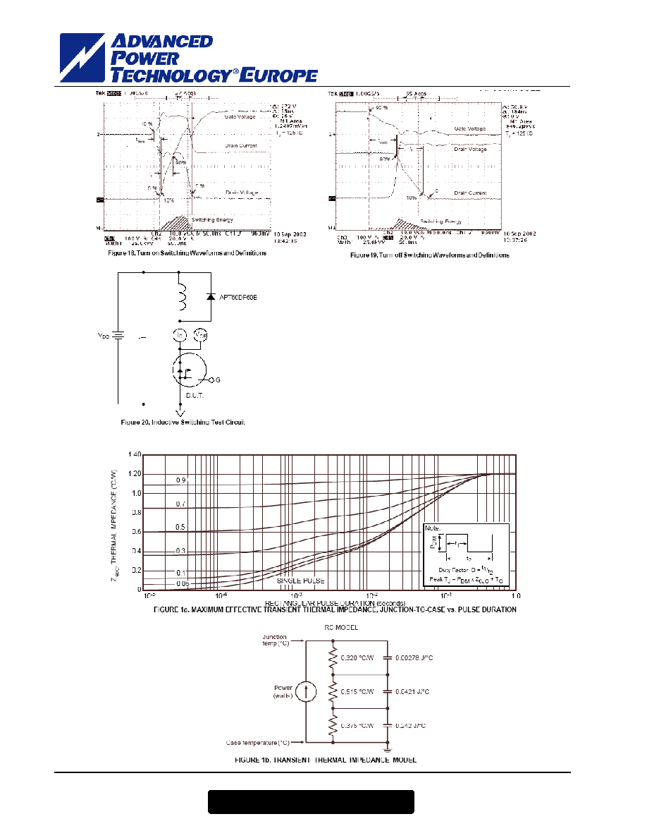
Thermal and package characteristics
Symbol Characteristic
Min Typ Max Unit
MOSFET
0.27
R
thJC
Junction
to
Case
Diode
1.21
R
thJA
Junction to Ambient (IGBT & Diode)
20
∞C/W
V
ISOL
RMS Isolation Voltage, any terminal to case t =1 min, I isol<1mA, 50/60Hz
2500 V
T
J
,T
STG
Storage
Temperature
Range
-55
150
T
L
Max Lead Temp for Soldering:0.063" from case for 10 sec
300
∞C
Torque Mounting
torque
(Mounting = 8-32 or 4mm Machine and terminals = 4mm Machine)
1.5
N.m
Wt Package
Weight
29.2 g
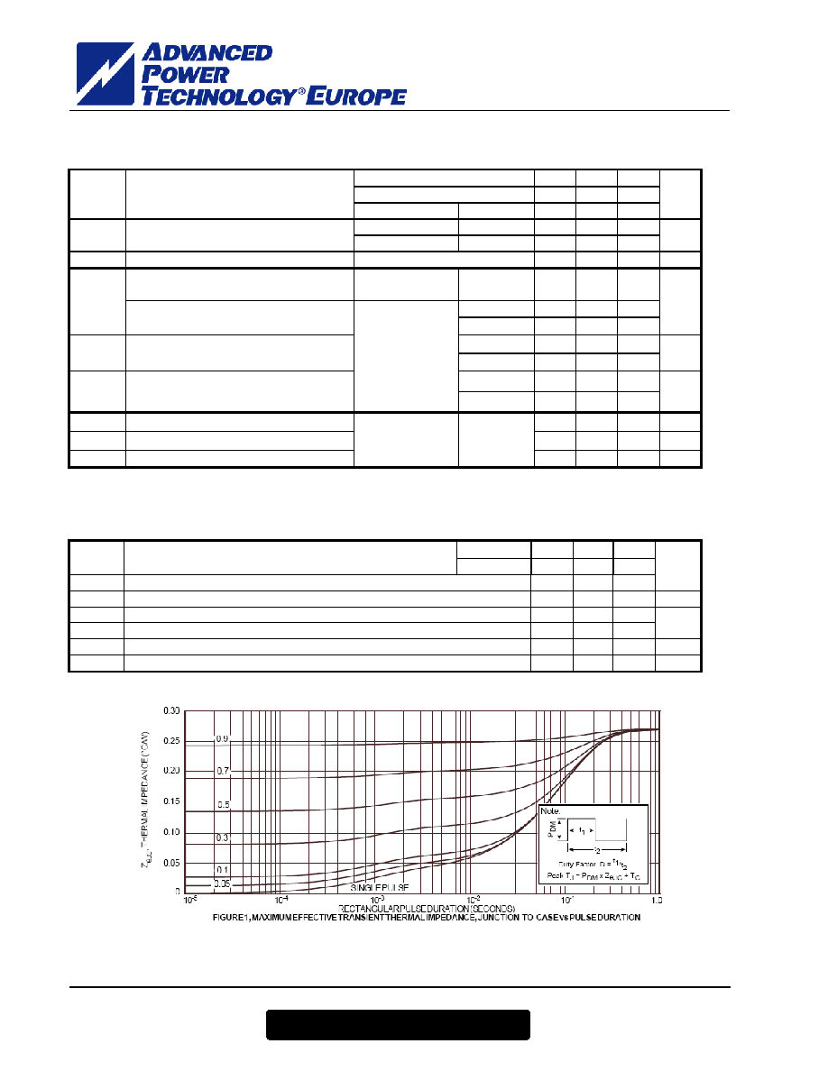
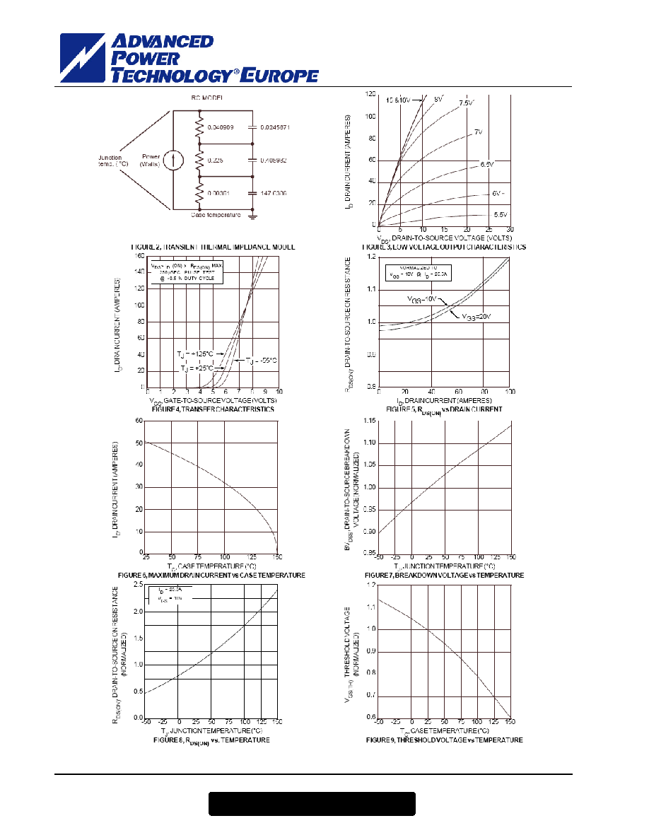
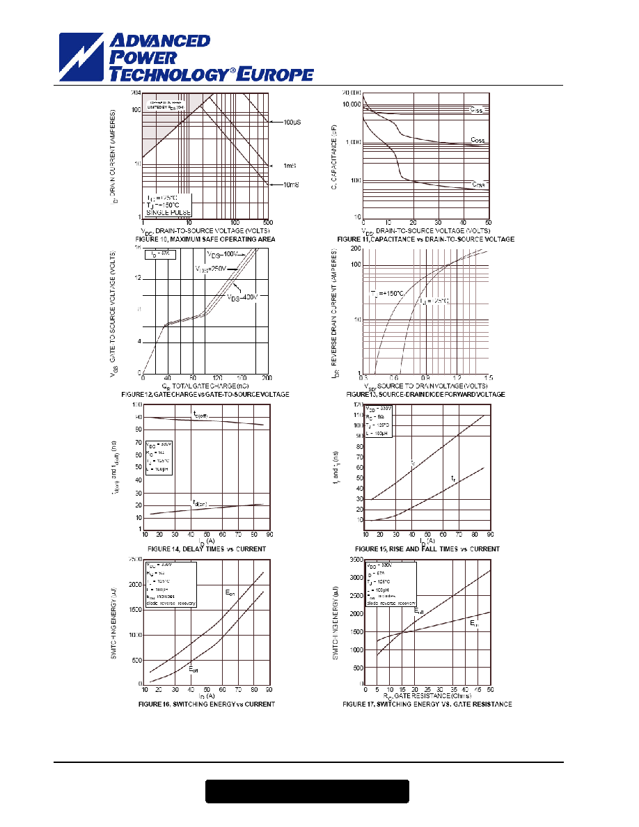
Typical
MOSFET
Performance Curve
APT50M75JLLU3
A
P
T
5
0M
75J
L
L
U
3 ≠ R
e
v 0
A
p
r
i
l
,
2004
APT website ≠ http://www.advancedpower.com
4 ≠ 8
APT50M75JLLU3
A
P
T
5
0M
75J
L
L
U
3 ≠ R
e
v 0
A
p
r
i
l
,
2004
APT website ≠ http://www.advancedpower.com
5 ≠ 8
APT50M75JLLU3
A
P
T
5
0M
75J
L
L
U
3 ≠ R
e
v 0
A
p
r
i
l
,
2004
APT website ≠ http://www.advancedpower.com
6 ≠ 8
Typical Diode Performance Curve
APT50M75JLLU3
A
P
T
5
0M
75J
L
L
U
3 ≠ R
e
v 0
A
p
r
i
l
,
2004
APT website ≠ http://www.advancedpower.com
7 ≠ 8
APT50M75JLLU3
A
P
T
5
0M
75J
L
L
U
3 ≠ R
e
v 0
A
p
r
i
l
,
2004
APT website ≠ http://www.advancedpower.com
8 ≠ 8
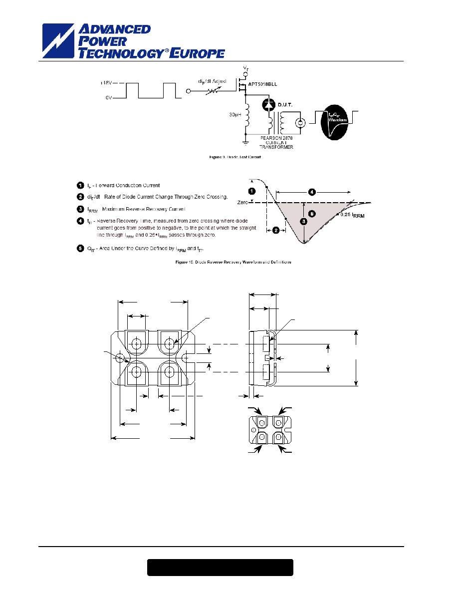
SOT-227 (ISOTOP
Æ
) Package Outline
31.5 (1.240)
31.7 (1.248)
Dimensions in Millimeters and (Inches)
7.8 (.307)
8.2 (.322)
30.1 (1.185)
30.3 (1.193)
38.0 (1.496)
38.2 (1.504)
14.9 (.587)
15.1 (.594)
11.8 (.463)
12.2 (.480)
8.9 (.350)
9.6 (.378)
Hex Nut M4
(4 places)
0.75 (.030)
0.85 (.033)
12.6 (.496)
12.8 (.504)
25.2 (0.992)
25.4 (1.000)
1.95 (.077)
2.14 (.084)
*
r = 4.0 (.157)
(2 places)
4.0 (.157)
4.2 (.165)
(2 places)
W=4.1 (.161)
W=4.3 (.169)
H=4.8 (.187)
H=4.9 (.193)
(4 places)
3.3 (.129)
3.6 (.143)
Emitter terminals are shorted
internally. Current handling
capability is equal for either
Emitter terminal.
ISOTOP
Æ
is a Registered Trademark of SGS Thomson
APT reserves the right to change, without notice, the specifications and information contained herein
APT's products are covered by one or more of U.S patents 4,895,810 5,045,903 5,089,434 5,182,234 5,019,522
5,262,336 6,503,786 5,256,583 4,748,103 5,283,202 5,231,474 5,434,095 5,528,058 and foreign patents. U.S and Foreign patents pending. All Rights Reserved.
Source
Gate
Drain
Anode