APTC60DDAM35T3
AP
T
C
6
0
DDAM
3
5
T
3
≠
R
e
v
1
J
u
n
e
,
2005
APT website ≠ http://www.advancedpower.com
1 - 6
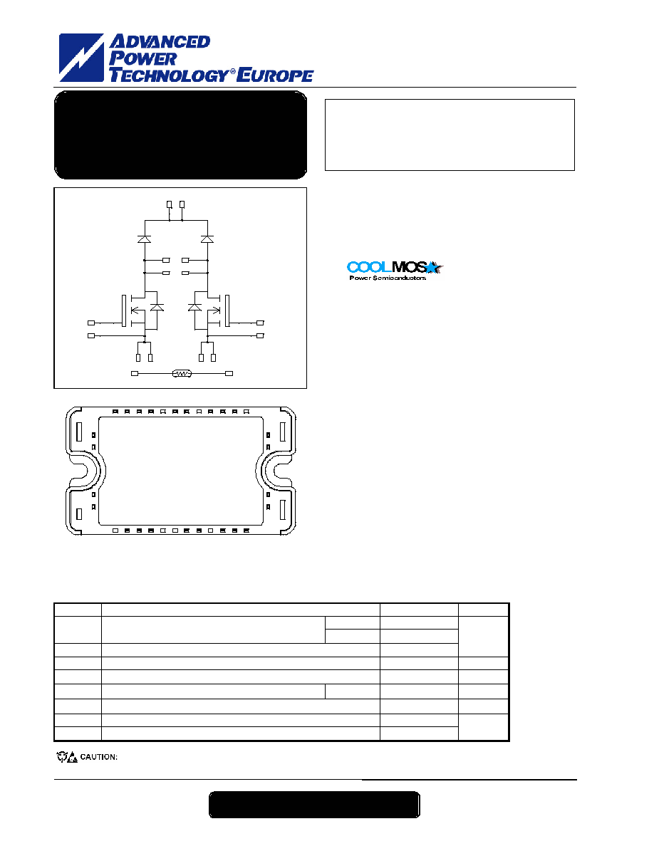
14
13
Q1
Q2
23
8
22
7
CR1
CR2
30
29
32
4
26
3
27
31
16
15
R1
16
15
18
20
23 22
13
11 12
14
8
7
29
30
28 27 26
3
32
31
10
19
2
25
4
All multiple inputs and outputs must be shorted together
Example: 13/14 ; 29/30 ; 22/23 ...
Absolute maximum ratings
These Devices are sensitive to Electrostatic Discharge. Proper Handing Procedures Should Be Followed.
Symbol Parameter
Max ratings
Unit
V
DSS
Drain - Source Breakdown Voltage
600
V
T
c
= 25∞C
72
I
D
Continuous
Drain
Current
T
c
= 80∞C
54
I
DM
Pulsed Drain current
200
A
V
GS
Gate - Source Voltage
±20
V
R
DSon
Drain - Source ON Resistance
35
m
P
D
Maximum Power Dissipation
T
c
= 25∞C
416
W
I
AR
Avalanche current (repetitive and non repetitive)
20
A
E
AR
Repetitive Avalanche Energy
1
E
AS
Single Pulse Avalanche Energy
1800
mJ
V
DSS
= 600V
R
DSon
= 35m
max @ Tj = 25∞C
I
D
= 72A @ Tc = 25∞C
Application
∑ AC and DC motor control
∑ Switched Mode Power Supplies
∑ Power Factor Correction
Features
∑
- Ultra low R
DSon
- Low Miller capacitance
- Ultra low gate charge
- Avalanche energy rated
- Very rugged
∑ Kelvin source for easy drive
∑ Very low stray inductance
- Symmetrical design
∑ Internal thermistor for temperature monitoring
∑ High level of integration
Benefits
∑ Outstanding performance at high frequency operation
∑ Direct mounting to heatsink (isolated package)
∑ Low junction to case thermal resistance
∑ Solderable terminals both for power and signal for
easy PCB mounting
∑ Low profile
∑ Each leg can be easily paralleled to achieve a single
boost of twice the current capability
Dual boost chopper
Super Junction MOSFET
Power Module
APTC60DDAM35T3
AP
T
C
6
0
DDAM
3
5
T
3
≠
R
e
v
1
J
u
n
e
,
2005
APT website ≠ http://www.advancedpower.com
2 - 6
All ratings @ T
j
= 25∞C unless otherwise specified
Electrical Characteristics
Symbol Characteristic
Test
Conditions
Min Typ Max Unit
BV
DSS
Drain - Source Breakdown Voltage V
GS
= 0V, I
D
= 375µA
600
V
V
GS
= 0V,V
DS
= 600V
T
j
= 25∞C
1
40
I
DSS
Zero Gate Voltage Drain Current
V
GS
= 0V,V
DS
= 600V
T
j
= 125∞C
375
µA
R
DS(on)
Drain ≠ Source on Resistance
V
GS
= 10V, I
D
= 72A
35
m
V
GS(th)
Gate
Threshold
Voltage
V
GS
= V
DS
, I
D
=
5.4mA
2.1 3 3.9 V
I
GSS
Gate ≠ Source Leakage Current
V
GS
= ±20
V, V
DS
= 0V
±150
nA
Dynamic Characteristics
Symbol Characteristic
Test
Conditions
Min Typ Max Unit
C
iss
Input
Capacitance
14
C
oss
Output
Capacitance
5.13
C
rss
Reverse Transfer Capacitance
V
GS
= 0V
V
DS
= 25V
f = 1MHz
0.42
nF
Q
g
Total gate Charge
518
Q
gs
Gate ≠ Source Charge
58
Q
gd
Gate ≠ Drain Charge
V
GS
= 10V
V
Bus
= 300V
I
D
= 72A
222
nC
T
d(on)
Turn-on
Delay
Time
21
T
r
Rise Time
30
T
d(off)
Turn-off Delay Time
283
T
f
Fall Time
Inductive Switching @ 125∞C
V
GS
= 15V
V
Bus
= 400V
I
D
= 72A
R
G
= 2.5
84
ns
E
on
Turn-on Switching Energy
1340
E
off
Turn-off Switching Energy
Inductive switching @ 25∞C
V
GS
= 15V, V
Bus
= 400V
I
D
= 72A,
R
G
= 2.5
1960
µJ
E
on
Turn-on Switching Energy
2192
E
off
Turn-off Switching Energy
Inductive switching @ 125∞C
V
GS
= 15V, V
Bus
= 400V
I
D
= 72A,
R
G
= 2.5
2412
µJ
Chopper diode ratings and characteristics
Symbol Characteristic
Test
Conditions
Min Typ Max Unit
V
RRM
Maximum Peak Repetitive Reverse Voltage
600
V
T
j
= 25∞C
250
I
RM
Maximum Reverse Leakage Current
V
R
=600V
T
j
= 125∞C
750
µA
I
F(A V)
Maximum Average Forward Current
50% duty cycle
T
c
= 70∞C
60
A
I
F
= 60A
2.2
2.7
I
F
= 120A
2.3
V
F
Diode Forward Voltage
I
F
= 60A
T
j
= 125∞C
1.4
V
T
j
= 25∞C
55
t
rr
Reverse Recovery Time
T
j
= 125∞C
151
ns
T
j
= 25∞C
121
Q
rr
Reverse Recovery Charge
I
F
= 60A
V
R
= 400V
di/dt=200A/µs
T
j
= 125∞C
999
nC
E
on
includes diode reverse recovery.
In accordance with JEDEC standard JESD24-1.
APTC60DDAM35T3
AP
T
C
6
0
DDAM
3
5
T
3
≠
R
e
v
1
J
u
n
e
,
2005
APT website ≠ http://www.advancedpower.com
3 - 6
Thermal and package characteristics
Symbol Characteristic
Min Typ Max Unit
IGBT 0.3
R
thJC
Junction
to
Case
Diode 0.9
∞C/W
V
ISOL
RMS Isolation Voltage, any terminal to case t =1 min, I isol<1mA, 50/60Hz
2500
V
T
J
Operating junction temperature range
-40 150
T
STG
Storage Temperature Range
-40
125
T
C
Operating Case Temperature
-40
100
∞C
Torque Mounting torque
To heatsink
M4
1.5
4.7
N.m
Wt Package
Weight
110 g
Temperature sensor NTC
(see application note APT0406 on www.advancedpower.com for more information).
Symbol Characteristic
Min Typ Max Unit
R
25
Resistance @ 25∞C
50
k
B
25/85
T
25
= 298.15 K
3952
K
-
=
T
T
B
R
R
T
1
1
exp
25
85
/
25
25
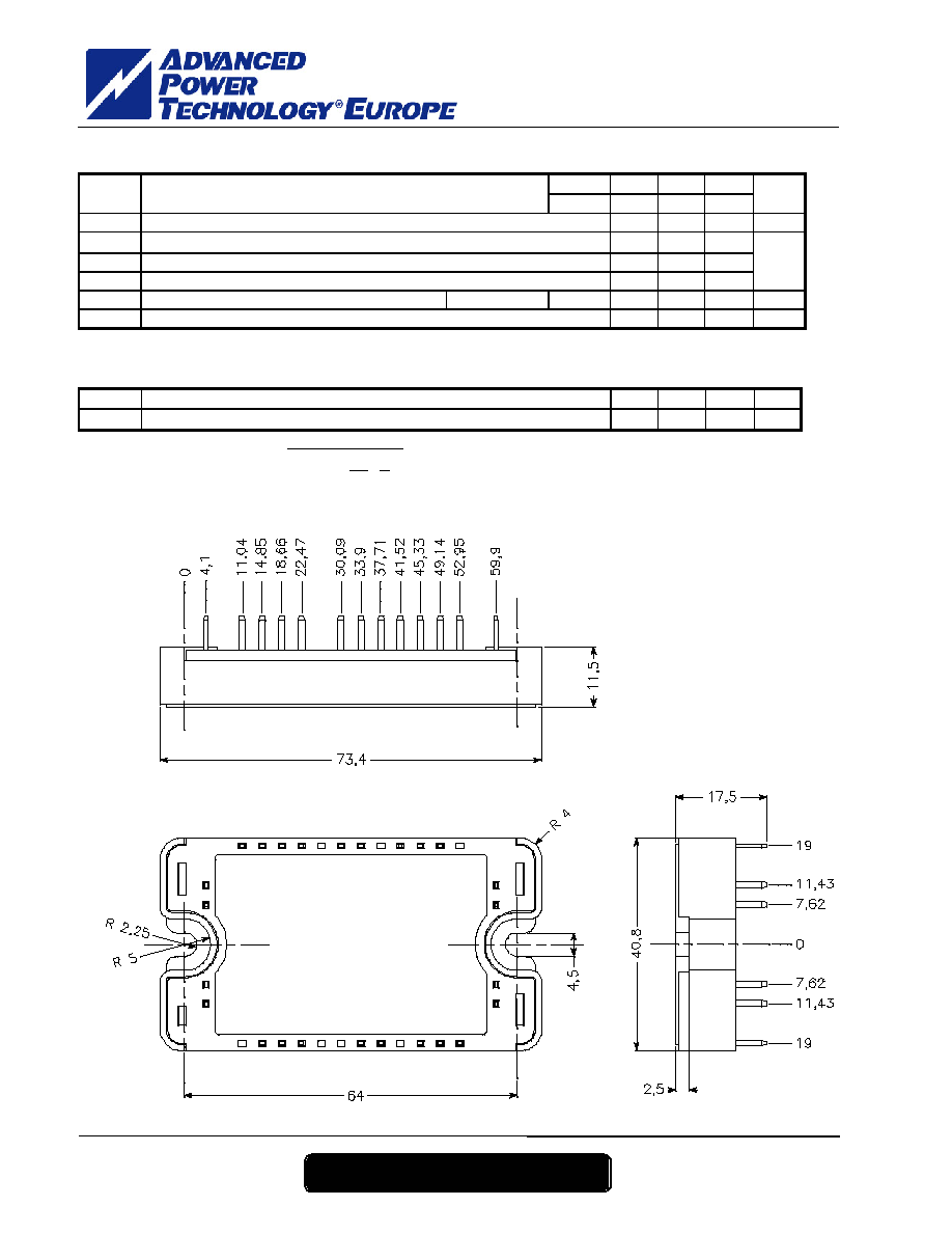
Package outline
(dimensions in mm)
17
12
28
1
T: Thermistor temperature
R
T
: Thermistor value at T
APTC60DDAM35T3
AP
T
C
6
0
DDAM
3
5
T
3
≠
R
e
v
1
J
u
n
e
,
2005
APT website ≠ http://www.advancedpower.com
4 - 6
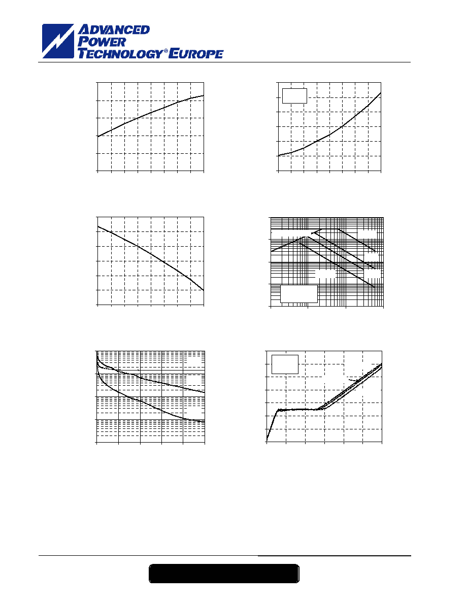
Typical Performance Curve
0.9
0.7
0.5
0.3
0.1
0.05
Single Pulse
0
0.05
0.1
0.15
0.2
0.25
0.3
0.35
0.00001
0.0001
0.001
0.01
0.1
1
10
rectangular Pulse Duration (Seconds)
The
r
m
a
l
I
m
pe
da
n
c
e
(
∞
C
/
W
)
Maximum Effective Transient Thermal Impedance, Junction to Case vs Pulse Duration
4V
4.5V
5V
5.5V
6V
6.5V
0
40
80
120
160
200
240
280
320
360
400
0
5
10
15
20
25
V
DS
, Drain to Source Voltage (V)
I
D
,
Dr
a
i
n
Cu
r
r
e
n
t
(
A
)
V
GS
=15&10V
Low Voltage Output Characteristics
Transfert Characteristics
T
J
=-55∞C
T
J
=25∞C
T
J
=125∞C
0
40
80
120
160
200
240
280
0
1
2
3
4
5
6
7
V
GS
, Gate to Source Voltage (V)
I
D
,
Dr
a
i
n
Cu
r
r
e
n
t
(
A
)
V
DS
> I
D
(on)xR
DS
(on)MAX
250µs pulse test @ < 0.5 duty cycle
R
DS
(on) vs Drain Current
V
GS
=10V
V
GS
=20V
0.9
0.95
1
1.05
1.1
0
20
40
60
80
100
120
I
D
, Drain Current (A)
R
DS
(
o
n
)
D
r
ai
n
t
o
S
o
u
r
ce O
N
R
esi
st
an
ce
Normalized to
V
GS
=10V @ 36A
0
10
20
30
40
50
60
70
80
25
50
75
100
125
150
T
C
, Case Temperature (∞C)
I
D
,
DC
D
r
a
i
n
Cu
r
r
e
n
t
(
A
)
DC Drain Current vs Case Temperature
APTC60DDAM35T3
AP
T
C
6
0
DDAM
3
5
T
3
≠
R
e
v
1
J
u
n
e
,
2005
APT website ≠ http://www.advancedpower.com
5 - 6
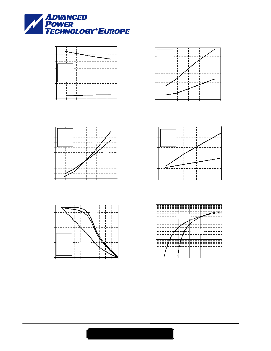
0.7
0.8
0.9
1.0
1.1
1.2
-50 -25
0
25 50 75 100 125 150
T
J
, Junction Temperature (∞C)
Breakdown Voltage vs Temperature
BV
DS
S
,
D
r
ai
n
t
o
S
o
u
r
ce B
r
eakd
o
w
n
V
o
l
t
ag
e (
N
o
r
m
a
l
i
z
e
d
)
ON resistance vs Temperature
0.0
0.5
1.0
1.5
2.0
2.5
3.0
-50 -25 0
25 50 75 100 125 150
T
J
, Junction Temperature (∞C)
R
DS
(
o
n
)
,
D
r
a
i
n
t
o
S
o
u
r
ce O
N
r
esi
st
an
ce
(
N
or
m
a
l
i
z
e
d)
V
GS
=10V
I
D
= 72A
Threshold Voltage vs Temperature
0.6
0.7
0.8
0.9
1.0
1.1
1.2
-50 -25
0
25 50 75 100 125 150
T
C
, Case Temperature (∞C)
V
GS
(
T
H
)
,
Thr
e
s
h
o
l
d
V
o
l
t
a
g
e
(
N
or
m
a
l
i
z
e
d)
Maximum Safe Operating Area
DC line
10 ms
1 ms
100 µs
0.1
1
10
100
1000
1
10
100
1000
V
DS
, Drain to Source Voltage (V)
I
D
,
D
r
a
i
n
C
u
r
r
e
nt
(
A
)
limited by R
DS
on
Single pulse
T
J
=150∞C
Ciss
Crss
Coss
10
100
1000
10000
100000
0
10
20
30
40
50
V
DS
, Drain to Source Voltage (V)
C
,
C
a
p
aci
t
a
n
ce (
p
F
)
Capacitance vs Drain to Source Voltage
V
DS
=120V
V
DS
=300V
V
DS
=480V
0
2
4
6
8
10
12
14
0
100
200
300
400
500
600
Gate Charge (nC)
V
GS
,
G
a
t
e
t
o
S
o
u
r
ce V
o
l
t
ag
e
(
V
)
Gate Charge vs Gate to Source Voltage
I
D
=72A
T
J
=25∞C
APTC60DDAM35T3
AP
T
C
6
0
DDAM
3
5
T
3
≠
R
e
v
1
J
u
n
e
,
2005
APT website ≠ http://www.advancedpower.com
6 - 6
T
J
=25∞C
T
J
=150∞C
1
10
100
1000
0.3
0.5
0.7
0.9
1.1
1.3
1.5
V
SD
, Source to Drain Voltage (V)
I
DR
,
R
ever
se
D
r
ai
n
C
u
r
r
en
t
(
A
)
Source to Drain Diode Forward Voltage
Delay Times vs Current
td(on)
td(off)
0
50
100
150
200
250
300
350
0
20
40
60
80
100 120
I
D
, Drain Current (A)
t
d(o
n
)
a
nd t
d(
off
)
(n
s
)
V
DS
=400V
R
G
=2.5
T
J
=125∞C
L=100µH
Rise and Fall times vs Current
t
r
t
f
0
20
40
60
80
100
120
0
20
40
60
80
100
120
I
D
, Drain Current (A)
t
r
a
nd t
f
(n
s
)
V
DS
=400V
R
G
=2.5
T
J
=125∞C
L=100µH
Switching Energy vs Current
E
on
E
off
0
0.5
1
1.5
2
2.5
3
3.5
4
4.5
5
0
20
40
60
80
100
120
I
D
, Drain Current (A)
S
w
it
c
h
in
g
E
n
e
r
g
y
(
m
J
)
V
DS
=400V
R
G
=2.5
T
J
=125∞C
L=100µH
E
on
E
off
0
2
4
6
8
10
0
5
10
15
20
25
Gate Resistance (Ohms)
S
w
i
t
ch
i
n
g
E
n
er
g
y
(
m
J)
Switching Energy vs Gate Resistance
V
DS
=400V
I
D
=72A
T
J
=125∞C
L=100µH
hard
switching
ZCS
ZVS
0
20
40
60
80
100
120
140
15 20 25 30 35 40 45 50 55 60 65
I
D
, Drain Current (A)
Fr
e
que
nc
y
(
k
H
z
)
Operating Frequency vs Drain Current
V
DS
=400V
D=50%
R
G
=2.5
T
J
=125∞C
T
C
=75∞C
"COOLMOSTM comprise a new family of transistors developed by Infineon Technologies AG. "COOLMOS" is a trademark of Infineon
Technologies AG".
APT reserves the right to change, without notice, the specifications and information contained herein
APT's products are covered by one or more of U.S patents 4,895,810 5,045,903 5,089,434 5,182,234 5,019,522
5,262,336 6,503,786 5,256,583 4,748,103 5,283,202 5,231,474 5,434,095 5,528,058 and foreign patents. U.S and Foreign patents pending. All Rights Reserved.