 | –≠–ª–µ–∫—Ç—Ä–æ–Ω–Ω—ã–π –∫–æ–º–ø–æ–Ω–µ–Ω—Ç: ACT4438-1 | –°–∫–∞—á–∞—Ç—å:  PDF PDF  ZIP ZIP |

CIRCUIT TECHNOLOGY
www.aeroflex.com
eroflex Circuit T
echnology
≠ Data Bus Modules For The Future © SCD4438-1 REV A 11/19/01
Features
∑ Transceiver meets military data bus requirements,
MIL-STD-1553 and MIL-STD-1760
∑ Low power dissipation at full output power
∑ Single +5V power supply
∑ Current Source Transmitter Output
∑ Bipolar Monolithic Construction
∑ Miniature Chipscale Package Bumped Chip Carrier
TM
(BCC++)
General Description
The Aeroflex Circuit Technology
Model ACT4438-1 is a next
generation monolithic transceiver
which provide full compliance with
MIL-STD-1553/1760 and data bus
requirements in a Bumped Chip
CarrierTM (BCC++) with the lowest
standby power consumption and
single power supply operation.
The Model ACT4438-1 performs the
front-end analog function of inputting
and outputting data through a
transformer to a MIL-STD-1553/1760
data bus with a few external
components.
Design of these transceivers reflects
particular attention to active filter
performance. This results in low bit
and word error rate with superior
waveform purity and minimal zero
crossover distortion. Efficient
transmitter electrical and thermal
design provides low internal power
dissipation and heat rise at high as
well as low duty cycles.
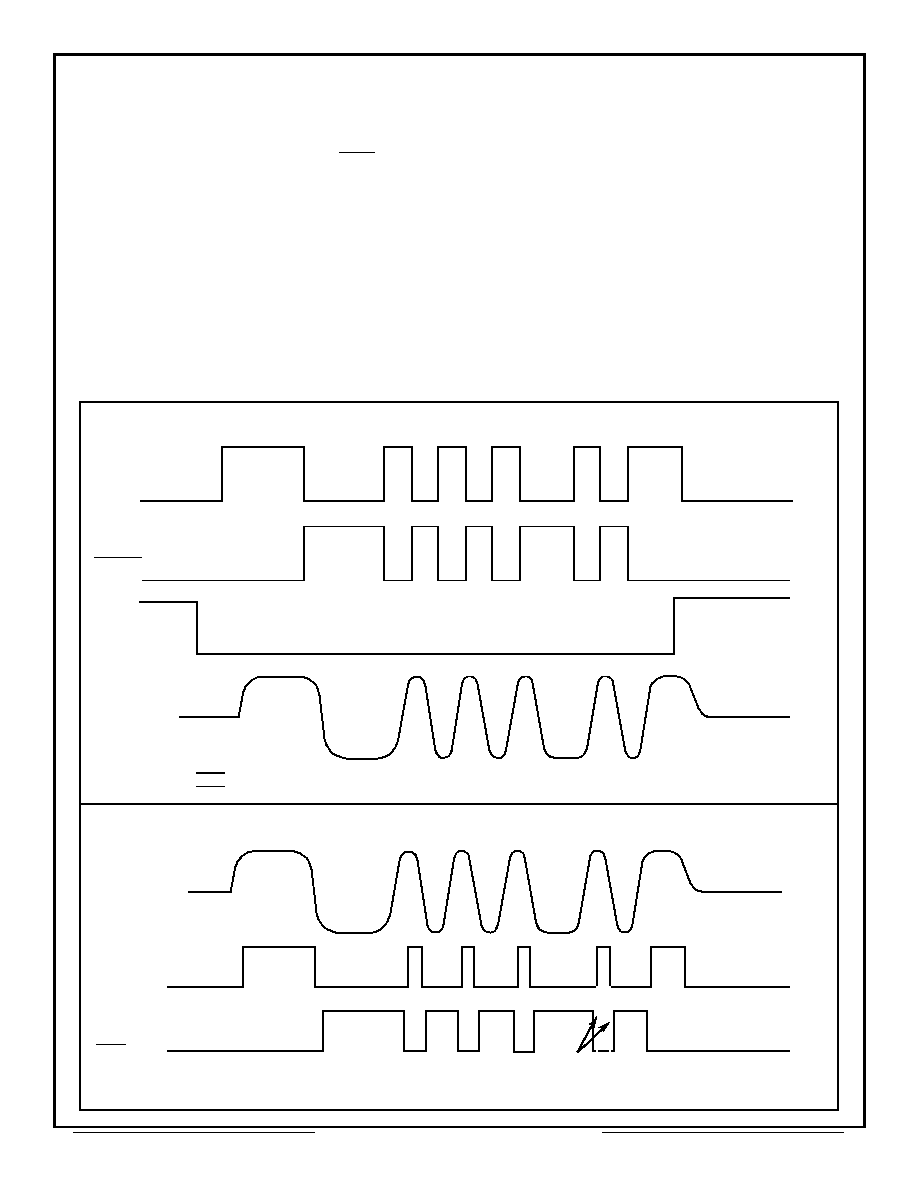
Transmitter
The Transmitter section accepts
bi-phase TTL data at the input and
when coupled to the data bus with a
1:2.5 transformer, isolated on the
data bus side with two 55 Ohm fault
isolation resistors for direct stub
coupling. The data bus signal
produced for RISET = 2.7K Ohm is
typically 7.5 Volts nominal P-P at
A-A', See Figure 5. When both DATA
and DATA inputs are held low, the
transmitter output becomes a high
impedance and is "removed" from the
line. In addition, an overriding
"INHIBIT" input provides for the
removal of the transmitter output from
the line. A logic "1" applied to the
"INHIBIT" takes priority over the
Block Diagram (without Transformer)
ACT4438≠1
Transceiver for MIL-STD-1553 / 1760
Preliminary
NOTE: BCC++ and Bumped Chip Carrier are Trademarks of Fujitsu Ltd.
SHAPING
OUTPUT
STAGE
COMP.
COMP.
REFERENCE
ACTIVE
FILTER
TX DATA IN
TX DATA IN
TX INHIBIT
+5 V
STROBE
RX DATA OUT
RX DATA OUT
GROUND
DRIVER
RISET
RX DATA IN
RX DATA IN
INPUT
AMP
TX DATA OUT
TX DATA OUT
in a Chipscale Package
Shown 2X
Aeroflex Circuit Technology
2
SCD4438-1 REV A 11/19/01 Plainview NY (516) 694-6700
condition of the data inputs and
disables the transmitter. (See
Transmitter Logic Waveform,
Figure 1.)
The transceiver utilizes an active
filter to suppress harmonics above
1MHz. The Transmitter may be
safely operated at 100% duty cycle
for an indefinite period into a short
circuited 1553 bus.
Receiver
The Receiver section accepts
bi-phase differential data at the input
and produces two TTL signals at the
output. The outputs are DATA and
DATA, and represent positive and
negative excursions of the input
beyond a pre-determined threshold.
(See Receiver Logic Waveform,
Figure 2.)
DATA IN
DATA IN
INHIBIT
LINE TO LINE
OUTPUT
NOTES:
1. DATA and DATA inputs must be complementary waveforms or 50% duty cycle average, with no delays between them.
2. DATA and DATA must be in the same state during off time (both high or low).
Figure 1. Transmitter Logic Waveforms
Figure 2. Receiver Logic Waveforms
Note overlap
NOTE
:
Waveforms shown are for normally low devices.
LINE TO LINE
INPUT
DATA OUT
DATA OUT
The pre-set internal thresholds will
detect data bus signals exceeding
1.150 Volts P-P and reject signals
less than 0.6 volts P-P when used
with a 1:2.5 turns ratio transformer.
(See Figure 5 for transformer data
and typical connection.)

Aeroflex Circuit Technology
3
SCD4438-1 REV A 11/19/01 Plainview NY (516) 694-6700
Absolute Maximum Ratings
Operating Case Temperature
-55∞C to +90∞C
Storage Case Temperature
-65∞C to +150∞C
Positive Power Supply Voltage
-0.3 V to +7.0 V
Receiver Differential Input
±10 V
Receiver Input Voltage (Common Mode)
±5 V
Driver Peak Output Current
650 mA
Total Package Power Dissipation over the full operating case
temperature rise at 100% duty cycle
2.2 Watt
Maximum Junction to Case temperature rise
44∞C
Thermal Resistance, Junction to bottom of case
20∞C/W
Electrical Characteristics ≠ Driver Section
Input Characteristics, TX DATA in or TX DATA in
Parameter
Condition
Symbol
Min
Typ
Max
Unit
"0" Input Current
V
IN
= 0.4 V
I
ILD
-
-0.2
-0.4
mA
"1" Input Current
V
IN
= 2.7 V
I
IHD
-
1
40
µA
"0" Input Voltage
V
IHD
-
-
0.7
V
"1" Input Voltage
V
IHD
2.0
-
-
V
Inhibit Characteristics
"0" Input Current
V
IN
= 0.4 V
I
ILI
-
-0.2
-0.4
mA
"1" Input Current
V
IN
= 2.7 V
I
IHI
-
1.0
40
µA
"0" Input Voltage
V
ILI
-
-
0.7
V
"1" Input Voltage
V
IHI
2
-
-
V
Delay from TX inhibit, (0
1) to inhibited output
t
DXOFF
-
150
300
nS
Delay from TX inhibit, (1
0) to active output
t
DXON
-
150
300
nS
Differential Output Noise, inhibit mode
V
NOI
-
2
10
mV p-p
Differential Output Impedance (inhibited)
Note 1
Z
OI
2K
-
-
Output Characteristics
Differential output level
R
L
= 35
V
O
6.5
7.5
8.0
V p-p
Rise and Fall Times
(10% to 90% of p-p output)
t
r
100
200
300
nS
Output Offset at point A-A' on Fig 5., 2.5 µS
after midpoint crossing of the parity bit of the
last word of a 660 µS message
R
L
= 35
V
OS
-
-
±90
mV peak
Delay from 50% point of TX DATA or TX DATA
input to zero crossing of differential signal
t
DTX
-
150
300
nS
Note 1. Power ON/OFF, measured from 75KHz to 1MHz at Point A-A. See Figure 5

Aeroflex Circuit Technology
4
SCD4438-1 REV A 11/19/01 Plainview NY (516) 694-6700
Note 2. V
cc
= 5 Volts ±0.1 V, for all measurements unless otherwise specified.
Note 3. Specifications apply over the case temperature range of -55∞C to +90∞C unless otherwise specfied.
Note 4. All typical values are measured at +25∞C.
Electrical Characteristics ≠ Receiver Section
Parameter
Condition
Symbol
Min
Typ
Max
Unit
Differential Voltage Range
V
IDR
-
-
20
V peak
Common Mode Rejection Ratio
CMRR
45
-
-
dB
Strobe Characteristics (Logic "0" inhibits output)
if not used, a 1K pullup to 5 V is recommended
"0" Input Current
V
S
= 0.4 V
I
IL
-
-0.2
-0.4
mA
"1" Input Current
V
S
= 2.7V
I
IH
-
1
+40
µA
"0" Input Voltage
V
IL
-
-
0.7
V
"1" Input Voltage
V
IH
2.0
-
-
V
Strobe Delay (turn-on)
t
SD(ON)
-
90
200
nS
Strobe Delay (turn-off)
t
SD(OFF)
-
90
200
nS
Threshold Characteristics (Sinewave input )
Input Threshold Voltage (Referred to the bus)
100KHz-
1MHz
V
TH
0.60
0.8
1.15
V p-p
Output Characteristics, RX DATA and RX DATA
"1" State
I
OH
= -0.4 mA
V
OH
2.5
3.7
-
V
"0" State
I
OL
= 4 mA
V
OL
-
0.3
0.5
V
Delay, (average)from differential input zero
crossings to RX DATA and RX DATA output
50% points
t
DRX
-
330
450
nS
Power Data
Maximum Currents, (+5V)
For RISET = 2.2 K
Duty Cycle
Typ
Max
Transmitter Standby
20 mA
30 mA
25% duty cycle
155 mA
185 mA
50% duty cycle
264 mA
335 mA
100% duty cycle
600 mA
650 mA
Power Supply Voltage
+V
4.75 to 5.5 Volts

Aeroflex Circuit Technology
5
SCD4438-1 REV A 11/19/01 Plainview NY (516) 694-6700
Figure 3 ≠ Transmitter (TX) Output Waveform
Figure 4 ≠ Transmitter (TX) Output Offset
Figure 5 ≠ Typical Transformer Connection
6V P-P MIN
7.7V P-P MAX
90%
10%
t
r
*
t
f
*
* Rise and fall times measured at point A-A' in Fig 5
0 Volts
OUTPUT OFFSET
*
OUTPUT OFFSET
*
LAST BIT
2.5 µsec
*Offset measured at point A-A' in Fig 5
A
A'
Z
O
Z
O
55
55
0 volts
Magnified View
3
1
Figure 6 ≠ Power Dissipation vs. Duty Cycle
P
O
W
E
R DI
S
S
I
P
A
T
I
O
N
M
I
L
L
IW
A
T
TS
Note: Vcc = 5 Volts, V
bus
(pt A-A') at 7.5 Volts P-P
10 20 30 40 50 60 70 80 90 100
1600
1400
1200
1000
800
600
400
200
0
DUTY CYCLE ≠ PERCENT
Z
O
Typical
Maximum
2
4
5
6
7
8
Use Pulse/Technitrol
Part# 1553-45 or equivalent
TX DATA OUT
TX DATA OUT
RX DATA IN
RX DATA IN
ACT4438-1
Transformer Model:
51
52
23-26
18-21
GND
RISET
2.7K
+5V
6.8µF
0.1µF
9,35,39,50
37
Direct Stub
1 :2.5
10,11,33,34
1800
2000
2200
Configurations and Ordering Information
Model No.
Screening Level
Receiver and Transmitter
Data Levels
(See Figure 1)
Case
ACT4438-1
Industrial Temperature
-55∞C to +90∞C
Normally Low
56 Bump Chip
Carrier