 | –≠–ª–µ–∫—Ç—Ä–æ–Ω–Ω—ã–π –∫–æ–º–ø–æ–Ω–µ–Ω—Ç: ACT5101-1 | –°–∫–∞—á–∞—Ç—å:  PDF PDF  ZIP ZIP |

CIRCUIT TECHNOLOGY
www.aeroflex.com
eroflex Circuit T
echnology
≠ Motor Driver Modules For The Future © SCD5101-1 REV D 5/14/01
Features
∑ 500 VDC RATING
∑ 40 AMP CONTINUOUS CURRENT (UP TO 85
∞
∞
∞
∞
C)
∑ PACKAGE SIZE 3.0" X 2.1" X 0.39"
∑ 4 QUADRANT CONTROL
∑ 6 STEP TRAPEZOIDAL DRIVE CAPABILITY
∑ MILITARY PROCESSING AVAILABLE
∑ MIL-PRF-38534 COMPLIANT CIRCUITS
AVAILABLE
∑ ISOLATED UPPER AND LOWER GATE DRIVERS
∑ FULL MILITARY (-55∞C TO +125∞C) TEMPERATURE
RANGE
General Description
The ACT5101-1 high voltage 3
phase brushless DC motor drive
combines a 500 VDC, 40A high
power output stage along with
low power digital input and gate
drive stages. A digital lock-out
feature protects the output stage
from accidental cross-conduction
thus preventing shoot-through
conditions. The ACT5101-1 also
includes a floating gate drive
design for each upper and lower
transistor. On-board gate drive
supplies provide a continuous
floating voltage for each upper
and lower transistor, even during a
motor stall.
The high power output stage
rated at 500 VDC, 40A is capable
of delivering over 20 kW to the
load even after derating. This is
accomplished through the use of
high power IGBTS with ultra-fast
recovery rectifiers in parallel.
The ACT5101-1 utilizes power
hybrid technology to provide the
highest levels of reliability and
lightest weight while requiring the
smallest amount of board space.
The ACT5101-1 is available with
military processing and operates
over the full -55 to +125 degrees C
temperature range.
This makes the ACT5101-1 ideal for
all military, space,and commercial
avionics' applications. These incl-
ude electro-hydrostatic actuators
[EHA's] and electro-mechanical
actuators [EMA's] for flight surface
control, missile fin actuators, thrust
vector control, electric brakes,
fuel and cooling pumps.
FIGURE 1 ≠ BLOCK DIAGRAM
Phase V+
Phase OUT
Phase RTN
+15V
SD
Ux
Lx
+15V
+15V
+15V
+15V
DC / AC
Converter
XFMR
Rect
&
XFMR
Rect
&
Optical
Isolation
To Other Sections
BRUSHLESS DC MOTOR DRIVE
ACT5101-1 HIGH VOLTAGE 3-PHASE

2
Aeroflex Circuit Technology
SCD5101-1 REV D 5/14/01 Plainview NY (516) 694-6700
Additional applications include environmental conditioning blowers, radar positioning, solar panel
positioning, and cryogenic cooler pumps. The ACT5101-1 is therefore especially suitable for use in
applications for all military tank upgrades, helicopters, planes and new commercial avionics using 270 VDC
as the main power.
50%
50%
90%
50%
10%
t
r
t
f
t
r
t
f
t
d
off
t
d
off
t
d
on
t
d
on
Ux INPUTS
LX INPUTS
PHASE
OUTPUTS
H
Z
Z
L
PHASE
OUTPUTS
t
SDU
t
SDL
UPPER TRANSISTOR
BEING SHUTDOWN
LOWER TRANSISTOR
BEING SHUTDOWN
FIGURE 2 ≠ TIMING DIAGRAM
SD
50%

3
Aeroflex Circuit Technology
SCD5101-1 REV D 5/14/01 Plainview NY (516) 694-6700
Table I ≠ Absolute Maximums
(T
C
= +25
∞
C unless otherwise specified)
PARAMETER
SYMBOL
RANGE
UNITS
SUPPLY VOLTAGE (PINS 3,7,11)
V+A,V+B,V+C
500
V DC
+15 V SUPPLY (PIN 12)
+15V
18
V DC
OUTPUT CURRENT
CONTINUOUS
lo
40
A
PULSED
l
op
60
A
CASE OPERATING TEMPERATURE
T
C
-55 to +125
∞
C
CASE STORAGE TEMPERATURE RANGE
T
CS
-55 to 150
∞
C
JUNCTION TEMPERATURE
T
J
150
∞
C
Table II ≠ Normal Operating Conditions
(T
C
= +25
∞
C unless otherwise specified)
PARAMETERS
SYMBOL
TEST
CONDITIONS
MIN
TYP
MAX
UNIT
POWER OUTPUT STAGE
Output Current Continuous
l
o
40
A
Supply Voltage
V+A,V+B,V+C
15
270
500
V DC
Output Voltage Drop (each IGBT)
V
CE(SAT)
lo = 40A
3.4
V DC
Instantaneous Forward Voltage
(flyback diode)
V
F
lop = 40A
(See Note 1)
2.4
V DC
Reverse Recovery Time (flyback diode)
t
rr
35
nsec
Reverse Leakage Current at Tc=25
∞
C
l
r
See Note 2
0.25
mA
Reverse Leakage Current at Tc=125
∞
C
l
r
8
mA
LOGIC INPUT SIGNALS (INTERNALLY PULLED UP) (V+ = 15V)
Input Voltage Low
V
INL
4
V DC
Input Voltage High
V
INH
6.8
V DC
Input Current Low
I
INH
3.75
mA

4
Aeroflex Circuit Technology
SCD5101-1 REV D 5/14/01 Plainview NY (516) 694-6700
SWITCHING CHARACTERISTICS
Upper Drive:
Turn-on propagation delay
t
d
(on)
700
nsec
Turn-off propagation delay
t
d
(off)
2
µsec
Shut-down propagation delay
t
SDU
3.5
µsec
Turn-on Transition Time
t
r
100
nsec
Turn-off Transition Time
t
f
250
nsec
Lower Drive:
Turn-on propagation delay
t
d
(on)
600
nsec
Turn-off propagation delay
t
d
(off)
2
µsec
Shut-down propagation delay
t
SDL
3.5
µsec
Turn-on Transition Time
t
r
250
nsec
Turn-off Transition Time
t
f
200
nsec
SWITCHING ENERGY LOSSES (At I = 40A, V = 480V)
Turn-on Energy
E
on
T
c
= +125
∞
C
4
mJ
Turn-off Energy
E
off
6
mJ
DEAD TIME
t
dt
500
nsec
THERMAL
Junction-Case Thermal Resistance (IGBT)
jcIGBT
each transistor
.45
∞
C/W
Junction-Case Thermal Resistance (DIODE)
jcDIODE
each diode
.85
∞
C/W
Maximum Lead Soldering Temp
T
S
See Note 3
250
∞
C
Junction Temperature Range
T
J
-55
150
∞
C
Case Operating Temperature
T
C
-55
125
∞
C
Case Storage Temperature
T
cs
-55
150
∞
C
NOTES:
1. Pulse width
300 usec duty cycle
2%
2. V+ = 480 V, Inputs = logic "1"
3. Solder 1/8" from case for 5 seconds maximum
Table II ≠ Normal Operating Conditions (Continued)
(T
C
= +25
∞
C unless otherwise specified)
PARAMETERS
SYMBOL
TEST
CONDITIONS
MIN
TYP
MAX
UNIT

5
Aeroflex Circuit Technology
SCD5101-1 REV D 5/14/01 Plainview NY (516) 694-6700
FUNCTION
PIN #
DESCRIPTION
V+ A
11
High Voltage D.C. Bus, Phase A
V+ B
7
High Voltage D.C. Bus, Phase B
V+ C
3
High Voltage D.C. Bus, Phase C
+15V
12
+15 VDC input required to power gate drive supply and gate drive circuitry of all
three phases.
GND
19,22,26
Reference for LOGIC supply, +15V supply, and digital inputs.
RTN A
8
Return for High Voltage Bus, Phase A.
RTN B
5
Return for High Voltage Bus, Phase B
RTN C
1
Return for High Voltage Bus, Phase C
PHASE A
9
Output to motor winding Phase A
PHASE B
6
Output to motor winding Phase B
PHASE C
2
Output to motor winding Phase C
UA
18
Digital input to Phase A upper transistor
LA
17
Digital input to Phase A lower transistor
UB
21
Digital input to Phase B upper transistor
LB
20
Digital input to Phase B lower transistor
UC
25
Digital input to Phase C upper transistor
LC
24
Digital input to Phase C lower transistor
SD
23
Digital shut-down input to enable / disable all six gate drives
N/C
4,10,13-16
No connection Internally
DIGITAL INPUT STAGE
The ACT5101-1 offers complete flexibility by allowing the user to turn on/off each of the 6 IGBTS in any order
or combination desired which enables the hybrid to be commutated in a 6 step trapezoidal mode. The only
unacceptable combination would be to turn on an upper and lower transistor of the same phase. This is not
a desirable condition for normal operation and is therefore not allowed. The ACT5101-1 has a digital lockout
feature that prevents turn-on of two in-line transistors. Damage to one or both of the transistors would occur
if this protection circuitry was not present in the hybrid. As a safety precaution, it is still recommended that a
500 nsec dead time be installed between commands at the inputs of the upper and lower transistors of the
same phase. This will compensate for any lag in transistor turn-off due to the inductive load.
The SD input allows the user to enable/disable the drive stage of the ACT5101-1 on demand. This input can
be incorporated into the user's temperature or current monitoring circuitry to shutdown the hybrid if
excessive current or case temperatures are sensed.
The digital input circuits are of the Schmitt trigger type with hystersesis of at least 1.6 volts, thus greatly
enhancing the input noise immunity. The inputs are internally pulled up to 15 volts so that an uncommitted
input is sensed as "OFF", providing a measure of protection against an accidental input disconnect.
GATE DRIVE
The ACT5101-1 includes a gate drive supply which provides a floating voltage for each upper and lower
transistor. This constant voltage allows the motor to be operated at very low duty cycles or driven into a stall
without any loss of upper or lower gate drive. This performance could not be obtained with only a
conventional boot strap design.

6
Aeroflex Circuit Technology
SCD5101-1 REV D 5/14/01 Plainview NY (516) 694-6700
POWER OUTPUT STAGE
IGBTS [insulated gate bipolar transistors] are technically similar to bipolars and MOSFETS. An IGBT is a
composite of a transistor with an N-channel MOSFET connected to the base of a PNP transistor. Like the
MOSFET, it offers high input impedance and requires low input drive current. IGBT conduction losses are low,
as with bipolar technology, and IGBT voltage drops are much lower compared with those of MOSFETs.
Consequently, the IGBT offers a high current density. With a smaller die size than the MOSFET, it can handle
the same current rating. Unlike MOSFETS, IGBTS have no intrinsic body diode. The ACT5101-1 includes 35 nsec
fast recovery rectifiers in parallel across each of the 6 IGBTS to carry the reverse current when the IGBT is
turned off.
It is important for the user to observe the Absolute Maximum ratings of the ACT5101-1 so that the voltage
and current rating is not exceeded. If over-voltage/over-current protection is desired it must be
implemented external to the ACT5101-1. Figure 3 shows the ACT5101-1 output current capability vs. case
temperature.
FIGURE 3 - OUTPUT CURRENT VS. CASE TEMPERATURE
POWER DISSIPATION
Power dissipation in the ACT5101-1 is composed of three elements: IGBT conduction losses, IGBT switching
losses, and commutation diode conduction losses. It is important that the user calculates power dissipations
over the full range of operating conditions of the hybrid, and uses these dissipations to compute the worst
case junction temperatures both for the IGBTs and diodes. The 150
∞
C maximum junction temperature
shown in Table 2 must not be exceeded. Additionally, program specific derating and reliability constraints
may require lower junction temperatures than the 150
∞
C maximum.
Calculating IGBT conduction losses requires the user to determine load profiles for the hybrid both in
current and time duration. IGBT collector-emitter voltage drops are shown in Figure 4.
0
20
40
60
80
100 120 140
10
15
20
25
30
35
40
45
Case Temperature T
C
(
∞C)
O
u
tpu
t
C
u
rre
n
t
I
O
(A
)

7
Aeroflex Circuit Technology
SCD5101-1 REV D 5/14/01 Plainview NY (516) 694-6700
FIGURE 4 - IGBT COLLECTOR-TO-EMITTER VOLTAGE VS. COLLECTOR CURRENT
Based upon this voltage drop and the conduction duty cycle a conduction power loss may be calculated
as:
where:
p
c
=
Conduction IGBT Power Dissipation
s
=
Switch Duty Cycle, (.33 for brushless drives in run condition, 1 in stall)
PWM
=
PWM on/off ratio
V
CE
=
Collector Emitter voltage from Figure 4 for a particular collector current
I
C
=
Collector current
Switching losses are dependent upon the operating frequency, collector current and again duty cycle as:
where:
P
s
=
Switching IGBT Power Dissipation
E
on
=
Turn on energy loss from Table 2
E
off
=
Turn off energy loss from Table 2
f
o
=
Pulse width modulation frequency
I
C
=
Collector current
Commutation diode losses are calculated as:
80
70
60
50
40
30
20
10
1.6
1.4
1.2
1.0
2.4
2.2
2.0
1.8
2.8
2.6
I
C
(A)
V
CE
(V)
T
J
= 150
∞
C
T
J
= 25
∞
C
P
c
S
PWM
V
CE
I
C
=
P
s
S
E
on
E
off
+
[
] f
o
I
C
40
------
=
P
d
s
1
PWM
≠
[
] V
f
I
f
=

8
Aeroflex Circuit Technology
SCD5101-1 REV D 5/14/01 Plainview NY (516) 694-6700
where:
P
d
=
Commutation diode losses
V
f
=
Commutation diode forward voltage from Figure 5
I
f
=
Commutation diode current
FIGURE 5 - DIODE VOLTAGE DROP VS. FORWARD CURRENT
Once the dissipations are calculated the junction temperatures may then be computed by summing the
conduction losses and switching losses for the IGBT and the commutation diode loss and multiplying these
dissipations by the respective junction to case thermal resistance as shown below:
where:
T
jIGBT
=
IGBT Junction Temperature
T
jDIODE
=
Commutation Diode Junction Temperature
jcIGBT
=
IGBT Thermal resistance from Table 2
jcDIODE
=
Diode Thermal resistance from Table 2
T
case
=
Case temperature
It is important that the user calculate junction temperatures over the full range of operating conditions,
including maximum load and stall conditions. Typically, hybrid losses peak at just maximum load with duty
cycles approaching, but just under, unity. Single transistor and diode losses peak under stall conditions since
power is dissipated in just one channel.
EXAMPLE
As a typical application consider a 10 HP brushless DC motor operating off a 270V line in a pump
application. The drive is trapezoidal, and the nominal load current will be 30 A. The system current limit is set
to roll back the PWM to maintain a maximum load current of 25 amperes in the event of a stall. Maximum
case temperature will be 85 C. Duty cycles may approach unity, but at stall it will be approximately 0.1.
PWM frequency is 20 kHz.
I
f
(A)
V
f
(V)
T
J
= 25
∞
C
T
J
= 150
∞
C
80
70
60
50
40
30
20
10
1.2
1.0
0.8
0.6
1.8
1.6
1.4
0
T
jIGBT
P
c
P
s
+
[
]
jcIGBT
T
C
+
=
T
jDIODE
P
d
jcDIODE
T
C
+
=

9
Aeroflex Circuit Technology
SCD5101-1 REV D 5/14/01 Plainview NY (516) 694-6700
At a run condition each transistor will be on for 120 degrees; then
Maximum hybrid dissipation is:
S
0.33
=
PWM
1
=
V
CE
1.6 V
=
I
C
30 A
=
P
c
S
PWM
V
CE
I
C
=
P
c
0.33 1.6 30
=
P
c
15.8 W
=
P
s
S
E
on
E
off
+
[
] f
o
I
C
40
------
=
E
on
0.004 J
=
E
off
0.006 J
=
f
o
20000 Hz
=
P
s
0.33
0.004
0.006
+
[
] 20000
30
40
------
=
P
s
49.5 W
=
T
jIGBT
P
c
P
s
+
[
]
jcIGB T
T
C
+
=
T
jIGBT
15.8
49.5
+
[
] 0.45∞ 85∞
+
=
T
jIGBT
114.4
∞ C
=
jcIGBT
0.45
∞C/W
=
T
C
85
∞ C
=
P
HYBRID
6 P
s
P
c
+
[
]
=
P
HYBRID
6 49.5
15.8
+
[
]
=
P
HYBRID
391.8 W
=

10
Aeroflex Circuit Technology
SCD5101-1 REV D 5/14/01 Plainview NY (516) 694-6700
At stall only two elements will be on, and they will be on full time.
S
1
=
PWM
0.1
=
V
CE
1.6 V
=
I
C
25 A
=
P
c
S
PWM
V
CE
I
C
=
P
c
1 0.1 1.6 25
=
P
c
4.0 W
=
P
s
S
E
on
E
off
+
[
] f
o
I
C
40
------
=
E
on
0.004 J
=
E
off
0.006 J
=
f
o
20000 Hz
=
P
s
1
0.004
0.006
+
[
] 20000
25
40
------
=
P
s
125 W
=
P
d
s
1
PWM
≠
[
] V
f
I
f
=
I
F
25 A
=
V
f
1.3 V
=
P
d
29.25 W
=
P
d
1
1
0.1
≠
[
] 1.3 25
=
T
jIGBT
P
c
P
s
+
[
]
jcIGBT
T
C
+
=
T
jIGBT
4
125
+
[
] 0.45∞ 85∞
+
=
T
jIGBT
143
∞ C
=
jcIGBT
0.45
∞C/W
=
T
C
85
∞ C
=

11
Aeroflex Circuit Technology
SCD5101-1 REV D 5/14/01 Plainview NY (516) 694-6700
MECHANICAL
The ACT5101-1 construction utilizes only the highest quality materials and manufacturing available to
ensure a high reliability, robust power hybrid design. The case is selected for best thermal conductivity,
hermeticity, and voltage/current carrying capability. The case is electrically isolated from the circuit and
can withstand 1500 VAC from pin to case, and input pins to output pins, therefore no insulating pads or
washers are required for mounting.
In order to remove the heat being generated from the ACT5101-1, it must be bolted down to the motor, a
heat sink or the actual system chassis such as a missile structure or aircraft wing rib for example. Thermally
conductive grease or a "Sil-pad" is recommended between the hybrid case baseplate and its mounting
surface to fill in any surface imperfections and improve the heat transfer from case-to-heat sink. It is
important to keep the temperature at this interface no greater than +125 degrees C in order to maintain
safe semi-conductor junction temperatures.
The leads of the ACT5101-1 can be formed upward, away from the baseplate, so that a PC board can be
mounted directly above it. A wiring harness can also be hand-wired and soldered directly to the leads of
the ACT5101-1 if this is preferred.
T
jDIODE
P
d
[ ]
jcDIODE
T
C
+
=
T
jDIODE
29.25 0.85
∞ 85∞
+
=
T
jDIODE
109.9
∞ C
=
jc DIODE
0.85
∞C/W
=
T
C
85
∞ C
=
P
HYBRID
2 P
s
P
c
P
d
+
+
[
]
=
P
HYBRID
2 125
4
29.25
+
+
[
]
=
P
HYBRID
316.5 W
=
Maximum hybrid dissipation will be:
12
Aeroflex Circuit Technology
SCD5101-1 REV D 5/14/01 Plainview NY (516) 694-6700
PIN
FUNCTION
PIN
FUNCTION
1
RTN C
26
GND
2
PHASE C
25
UC
3
V + C
24
LC
4
N/C
23
SD
5
RTN B
22
GND
6
PHASE B
21
UB
7
V + B
20
LB
8
RTN A
19
GND
9
PHASE A
18
UA
10
N/C
17
LA
11
V + A
16
N/C
12
+15 V
15
N/C
13
N/C
14
N/C
INPUTS
OUTPUTS
PHASE A PHASE B PHASE C
UA
UB
UC
LA
LB
LC
SD
1
1
1
1
1
1
1
1
1
0
0
0
0
0
0
0
0
0
1
1
1
0
0
0
0
0
0
1
1
1
1
1
1
0
0
0
0
0
0
1
1
1
0
0
0
1
1
1
0
0
0
1
1
1
1
0
0
1
0
0
0
0
0
1
1
1
1
1
0
1
1
0
0
1
0
1
1
1
1
1
0
1
0
0
0
0
0
1
0
1
1
1
1
0
1
0
1
0
1
0
1
0
1
0
1
0
0
0
0
0
0
0
0
0
0
0
0
0
0
0
0
0
0
0
0
0
Z
L
L
Z
L
L
L
L
L
H
H
H
H
H
Z
H
H
Z
L
Z
L
H
H
H
H
H
Z
Z
L
L
L
L
L
H
Z
H
H
H
H
L
Z
L
H
Z
H
L
Z
L
H
Z
H
L
L
L
1
1
0
1
1
0
1
1
0
1
0
1
1
0
1
1
0
1
0
0
0
Z
L
H
Z
L
H
Z
L
H
X
X
X
X
X
X
1
Z
Z
Z
H=high level, L=low level, X=irrelevant, Z=high impedance (off)
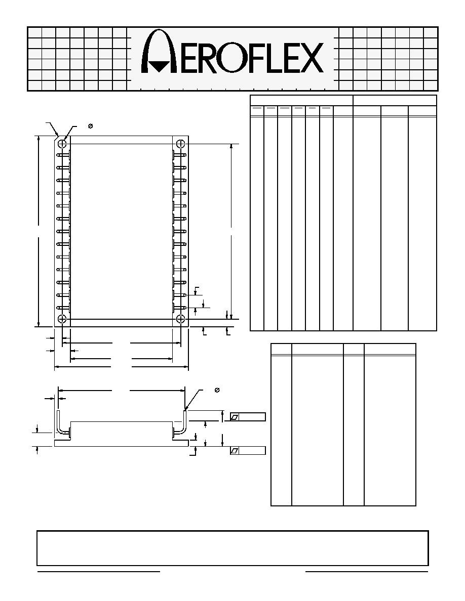
2.100
1.600
.250
.120
1.860
3.000
.125
2.750
.300
.057
2.010
.330
4X .128 -.005,+.002 THRU
26X .048 - .052
13
14
26
.54-.58
1
The information contained in this data sheet is believed to be accurate; however, Aeroflex Laboratories Incorporated assumes no
responsibility for its use, and no license or rights are granted by implication or othewise in connection therewith.
Aeroflex Circuit Technology
35 South Service Road
Plainview New York 11803
FAX: (516) 694-6715
Toll Free Inquiries: 1-(800) 843-1553
Telephone: (516) 694-6700
Specifications subject to change without notice
C I R C U I T T E C H N O L O G Y
12X .200
Power Package Outline
.050
Notes:
1. Package contains BeO substrate.
2. Dimensions Tolerance: ±.005, unless otherwise noted.
±.020
.165
Chamfer
.035-.065 X 45∞
See note 3
3. Pin Tolerance: non-cumulative
.003IN/IN
.003IN/IN