 | –≠–ª–µ–∫—Ç—Ä–æ–Ω–Ω—ã–π –∫–æ–º–ø–æ–Ω–µ–Ω—Ç: ACT5260 | –°–∫–∞—á–∞—Ç—å:  PDF PDF  ZIP ZIP |
eroflex Circuit Technology ≠ RISC TurboEngines For The Future © 9/15/97 SCD5260PC REV A
s
Allows potentially higher pipeline clock rates due to it multiplication of the input clock
by 2,3,4,5,6,7 or 8 compared to the 4XXX series method of multiplying the input clock
by only 2, then dividing it down by 2,3,4 etc for output system clock.
s
The RM5260 is a 3.3 volt device with 5 volt tolerant I/O's.
s
It has a fully operational IEEE 1149.1 JTAG boundary scan interface.
s
On-board supply de-coupling capacitors and PLL filter network.
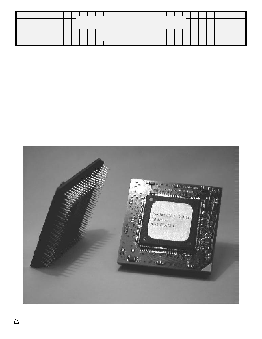
The Aeroflex ACT5260PC-P10-POD adapts a QED RM5260 MIPS microprocessor to an R4400PC,
R4600 or R4700 processor's 179 pin PGA footprint. This product allows the evaluation of the latest
MIPS IV 5XXX series performance in existing 4XXX series hardware. Some of the performance
enhancements include:
ACT5260 FR4 Adapter
ACT5260PC-P10-POD
FR4 Adapter

Aeroflex Circuit Technology
SCD5260PC REV A 9/15/97 Plainview NY (516) 694-6700
2
ACT5260 DESCRIPTION:
The ACT5260 is a highly integrated superscalar
microprocessor that implements a superset of the
MIPS IV Instruction Set Architecture(ISA). It has a
high performance 64-bit integer unit, a high
throughput, fully pipelined 64-bit floating point unit,
an operating system friendly memory management
unit with a 48-entry fully associative TLB, a 16 KByte
2-way set associative instruction cache, a 16 KByte
2-way set associative data cache, and a
high-performance 64-bit system interface. The
ACT5260 can issue both an integer and a floating
point instruction in the same cycle.
The ACT5260 is ideally suited for high-end
embedded control applications such as
internetworking, high performance image
manipulation, high speed printing, and 3-D
visualization.
HARDWARE OVERVIEW
The ACT5260 offers a high-level of integration
targeted at high-performance embedded
applications. Some of the key elements of the
ACT5260 are briefly described below.
Superscalar Dispatch
The ACT5260 has an efficient asymmetric
superscalar dispatch unit which allows it to issue an
integer instruction and a floating-point computation
instruction simultaneously. With respect to
superscalar issue, integer instructions include alu,
branch, load/store, and floating-point load/store,
while floating-point computation instructions include
floating-point add, subtract, combined multiply-add,
converts, etc. In combination with its high throughput
fully pipelined floating-point execution unit, the
superscalar capability of the ACT5260 provides
unparalleled price/performance in computationally
intensive embedded applications.
CPU Registers
Like all MIPS ISA processors, the ACT5260 CPU
has a simple, clean user visible state consisting of 32
general purpose registers, two special purpose
registers for integer multiplication and division, a
program counter, and no condition code bits.
Pipeline
For integer operations, loads, stores, and other
non-floating-point operations, the ACT5260 uses the
simple 5-stage pipeline also found in the circuits
R4600, R4700, and R5000. In addition to this
standard pipeline, the ACT5260 uses an extended
seven stage pipeline for floating-point operations.
Like the R5000, the ACT5260 does virtual to physical
translation in parallel with cache access.
Integer Unit
Like the R5000, the ACT5260 implements the
MIPS IV Instruction Set Architecture, and is therefore
fully upward compatible with applications that run on
processors implementing the earlier generation
MIPS I-III instruction sets. Additionally, the ACT5260
includes two implementation specific instructions not
found in the baseline MIPS IV ISA but that are useful
in the embedded market place. Described in detail in
a later section, these instructions are integer
multiply-accumulate and 3-operand integer multiply.
The ACT5260 integer unit includes thirty-two
general purpose 64-bit registers, a load/store
architecture with single cycle ALU operations (add,
sub, logical, shift) and an autonomous multiply/divide
unit. Additional register resources include: the HI/LO
result registers for the two-operand integer multiply/
divide operations, and the program counter(PC).
Register File
The ACT5260 has thirty-two general purpose
registers with register location 0 hard wired to zero.
These registers are used for scalar integer
operations and address calculation. The register file
has two read ports and one write port and is fully
bypassed to minimize operation latency in the
pipeline.
ALU
The ACT5260 ALU consists of the integer adder/
subtractor, the logic unit, and the shifter. The adder
performs address calculations in addition to
arithmetic operations, the logic unit performs all
logical and zero shift data moves, and the shifter
performs shifts and store alignment operations. Each
of these units is optimized to perform all operations in
a single processor cycle
For Detail Information regarding the operation of
the Quantum Effect Design (QED) RISCMark
TM
RM5260
TM
, 64-Bit Superscalar Microprocessor see
the QED datasheet.

Aeroflex Circuit Technology
SCD5260PC REV A 9/15/97 Plainview NY (516) 694-6700
3
Although the device has a 4XXX PC 179 pin
PGA compatible footprint, it is not a drop-in
replacement since the RM5260 has a different
clocking scheme. The RM5260 does not
generate the system clocks the same as the
R4400, R4600 and R4700. Instead, the system
clock is an input, which is multiplied up to the
pipeline rate. On the adapter, the Tclock and
Rclock pins are floating; not connected to
anything. SYNCout and IOout are connected to
ground to commit possible unconnected CMOS
inputs to a level. Depending on the system
configuration, accommodating the clocking
difference can be as simple as a few re-routing
jumpers or generating divisors of the original
MasterClock and the addition of some
phase-skewing buffers to emulate the Rclock
and Tclock system clocks. In addition, the boot
time mode bit serial stream needs to be
scrutinized before plugging in a RM5260 into an
R4700 or R4400 socket. The R4700 is closest
to the RM5260 whereas the R4400 is quite
different.
Figure 2 is an example of what had to be done
to an Algorithmics P4000i (IDT79S460) Single
Board Computer which was originally configured
for an R4700 with a 50 MHz input clock (100
MHz pipeline) and a divide by 2 output clock (50
MHz bus rate). With three wire jumpers, the
ACT5260PC-P10-POD was up and running with
no changes to the boot and monitor PROM or
any recompilation of application programs. In
this case, the R4700's modebit stream
happened to be compatible, where a board
jumper used to change the output clocks (Tclock
and Rclock) from divide by 2 to divide by 3 had
the effect of changing the Pclock multiplier from
2 to 3, upping the pipeline rate up to 150 Mhz
without changing the board oscillator.
Application Considerations:
R4700
ACT5260PC
M
A
S
T
E
R
C
L
O
C
K
R
C
L
K
T
C
L
K
S
y
s
C
l
k
R
C
L
K
T
C
L
K
Oscillator
50MHz
Oscillator
50MHz
Figure 2 ≠ Setup Example
From
To

Aeroflex Circuit Technology
SCD5260PC REV A 9/15/97 Plainview NY (516) 694-6700
4
Boot Time Mode Stream Comparison Chart ≠ 5260 vs 4700
5260
4700
Mode Bit
Description
Mode Bit
Description
0
Reserved (must be zero)
0
Reserved: Must be zero (0)
4..1
Write-back data rate
0
DDDD
1
DDxDDx
2
DDxxDDxx
3
DxDxDxDx
4
DDxxxDDxxx
5
DDxxxxDDxxxx
6
DxxDxxDxxDxx
7
DDxxxxxxDDxxxxxx
8
DxxxDxxxDxxxDxxx
9-15
reserved
4..1
Write-back data rate
0
D
1
DDx
2
DDxx
3
DxDx
4
DDxxx
5
DDxxxx
6
DxxDxx
7
DDxxxxxx
8
DxxxDxxx
9-15
reserved
7..5
Pclock to SysClock Multiplier
0
Multiply by 2, 1
Multiply by 3
2
Multiply by 4, 3
Multiply by 5
4
Multiply by 6, 5
Multiply by 7
6
Multiply by 8, 7 reserved
7..5
Clock divisor
0
2,1
3
2
4, 3
5
4
6, 5
7
6
8, 7
reserved
8
Specifies byte ordering. Logically ORed with
BigEndian input signal.
0
Little endian
1
Big endian
8
0
Little endian
1
Big endian
10..9
00
R4000 compatible non-block writes,
01
reserved,
10
pipelined non-block writes,
11
non-block write re-issue
10..9
00
R4000 compatible,
01
reserved,
10
pipelined writes,
11
write re-issue
11
0
Enable the timer interrupt on Int[5],
1
Disable the timer interrupt on Int[5].
11
0
Enable the timer interrupt on Int[5],
1
Disable the timer interrupt on Int[5].
12
Reserved: Must be zero (0)
12
Reserved: Must be zero (0)
14..13
Output driver strength
10
100% strength (fastest), 11
83%
strength, 00
67% strength, 01
50%
strength (slowest)
14..13
Output driver strength
10
100% strength (fastest), 11
83%
strength, 00
67% strength, 01
50%
strength (slowest)
15
Reserved: Must be zero (0)
15
0
TClock[0] enabled,
1
TClock[0] disabled
17..16
System configuration identifiers - software
visible in processor Config[21..20]
16
0
TClock[1] enabled,
1
TClock[1] disabled
17
0
RClock[0] enabled,
1
RClock[0] disabled
18
0
Set Timer/Counter to run at Pclock/2
1
Set Timer/Counter to run at Pclock
18
0
RClock[1] enabled,
1
RClock[1] disabled
21..19
Reserved: Must be zero (0)
255..19
Reserved: Must be zero (0)
24..22
Write address to write data delay in P cycles
000
0 cycles(R5000), ..., 111
7 cycles
255..25
Reserved: Must be zero (0)
Aeroflex Circuit Technology
SCD5260PC REV A 9/15/97 Plainview NY (516) 694-6700
5
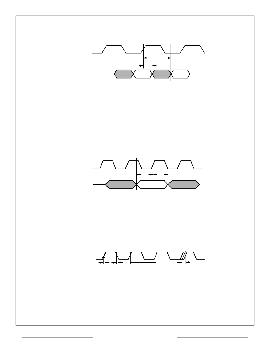
Figure 5 ≠ SysClock Timing
Figure 4 ≠ Input Timing
Figure 3 ≠ Output Timing
±t
JitterIn
t
SCRise
t
SCFall
SysClock
t
SCP
Data
SysClock
Data
t
DH
t
DS
Data
SysClock
Data
Data
t
DO
t
DO
MIN