Data Sheet
January 2002
CSP1027 Voice Band Codec for
Cellular Handset and Modem Applications
1 Features
s
-
(delta-sigma) A/D and D/A converters with stan-
dard 16-bit serial I/O interface.
s
On-chip filters meet ITU-T G.712 voice band fre-
quency response and signal to distortion plus noise
specifications. Suitable for IS-54, GSM, and JDC
digital cellular applications.
s
Low-profile package (<1.5 mm) 48-pin thin quad flat
pack (TQFP) available or 44-pin EIAJ quad flat pack
(QFP).
s
Operates in systems with a 3.0 V to 5.0 V digital
power supply and a 5.0 V analog supply.
s
Low-power 0.9 �m CMOS technology, fully static
design, typical power of 68 mW when active and
0.05 mW in standby with a 3.3 V digital supply and a
5.0 V analog supply.
s
A low-power inactive (standby) state without stop-
ping clock or removing power supply.
s
Sampling rates up to 24 kHz.
s
On-chip programmable sampling clock generator
allows input clock to be an integer multiple of
125 times the sampling rate or an integer multiple of
the sampling rate.
s
Programmable phase adjust of both codec sampling
clock and baseband codec clock.
s
Two on-chip clock dividers for generating the output
clock for the baseband codec and the output clock
for other processors.
s
Regulated microphone power supply.
s
Microphone preamplifier, with programmable input
ranges of 0.16 Vp-p and 0.5 Vp-p.
s
Output amplifier, with programmable gain settings,
0 dB to �45 dB in �3 dB steps.
s
High-pass filters selectable via control registers.
s
Power-on reset pulse generator.
s
Standard 16-bit serial I/O interface.
s
Serial I/O multiprocessor mode compatible with Agere
System Inc.'s DSP16A and DSP1610/1616/1617/1618
digital signal processors.
2 Description
The Agere CSP1027 is a high-precision linear voice
band
-
(delta-sigma) codec designed for cellular
handset and modem applications. The device is fabri-
cated in low-power CMOS technology and designed for
low-voltage (3.0 V to 5.0 V) digital systems. The
CSP1027 is packaged in a 44-pin EIAJ quad flat pack
(QFP) or a 48-pin EIAJ thin quad flat pack (TQFP). In
the 48-pin TQFP, the CSP1027 occupies a total volume
of 0.0784 cm
3
.
The CSP1027 has a variety of significant programmable
features not found in standard voice band codecs. The
analog interface includes a microphone preamplifier with
programmable gain settings, an output amplifier with
gain programmable in 3 dB steps over a 45 dB range,
and a regulated microphone power supply. An inactive
mode allows a low-power standby state, and a mute
function provides suppression of the analog output. On-
chip antialiasing and anti-imaging filtering includes a
selectable high-pass filter. The CSP1027 meets
ITU-T G.712 voice band specifications.
The programmable features of the CSP1027 are set by
writing four on-chip control registers through the serial
I/O interface. The codec's digital input/output uses a lin-
ear 16-bit two's complement data format that is also
transferred through the serial I/O interface. The
CSP1027 interfaces easily to the 16-bit serial ports of
digital signal processors and other devices. The serial
interface supports the Agere fixed-point DSP family
serial multiprocessor mode. This allows up to eight com-
patible devices, including two CSP1027s, to interface to
each other on a common 4-wire bus using a time-divi-
sion-multiplexing scheme.

CSP1027 Voice Band Codec for
Data Sheet
Cellular Handset and Modem Applications
January 2002
Agere Systems Inc.
2
Table of Contents
Contents
Page
1
Features ...................................................................................................................................................... 1
2
Description .................................................................................................................................................. 1
3
Pin Information ........................................................................................................................................... 3
4
Architectural Information ............................................................................................................................ 5
4.1
Overview........................................................................................................................................... 6
4.2
Description of Signal Paths............................................................................................................... 6
4.3
Programmable Features ................................................................................................................. 13
4.4
Power-On Reset ............................................................................................................................. 14
4.5
Clock Generation ............................................................................................................................ 16
4.6
Serial I/O Configurations................................................................................................................. 20
5
Register Information.................................................................................................................................. 26
5.1
Codec I/O Control 0 (cioc0) Register ............................................................................................. 26
5.2
Codec I/O Control 1 (cioc1) Register ............................................................................................. 27
5.3
Codec I/O Control 2 (cioc2) Register ............................................................................................. 28
5.4
Codec I/O Control 3 (cioc3) Register ............................................................................................. 29
6
Signal Descriptions ................................................................................................................................... 30
6.1
Clock Interface................................................................................................................................ 30
6.2
Reset Interface ............................................................................................................................... 31
6.3
Serial I/O Interface.......................................................................................................................... 31
6.4
External Gain Control Interface ...................................................................................................... 32
6.5
Digital Power and Ground............................................................................................................... 32
6.6
Analog Interface.............................................................................................................................. 32
6.7
Analog Power and Ground ............................................................................................................. 32
7
Application Information ............................................................................................................................. 33
7.1
Analog Information.......................................................................................................................... 33
7.2
Power Supply Configuration ........................................................................................................... 36
7.3
The Need for Fully Synchronous Operation ................................................................................... 36
7.4
Crystal Oscillator............................................................................................................................. 38
7.5
Programmable Clock Generation ................................................................................................... 45
8
Device Characteristics .............................................................................................................................. 47
8.1
Absolute Maximum Ratings ............................................................................................................ 47
8.2
Handling Precautions...................................................................................................................... 47
8.3
Recommended Operating Conditions............................................................................................. 47
9
Electrical Characteristics and Requirements ............................................................................................ 48
9.1
Power Dissipation ........................................................................................................................... 50
10 Analog Characteristics and Requirements................................................................................................ 51
10.1
Analog Input and Microphone Regulator ........................................................................................ 51
10.2
Analog-to-Digital Path..................................................................................................................... 52
10.3
Digital-to-Analog Path..................................................................................................................... 53
10.4
Miscellaneous ................................................................................................................................. 54
11 Timing Characteristics and Requirements ................................................................................................ 55
11.1
Clock Generation ............................................................................................................................ 56
11.2
Power-On Reset ............................................................................................................................. 57
11.3
Reset .............................................................................................................................................. 58
11.4
Serial I/O Communication .............................................................................................................. 59
11.5
Serial Multiprocessor Communication ............................................................................................ 61
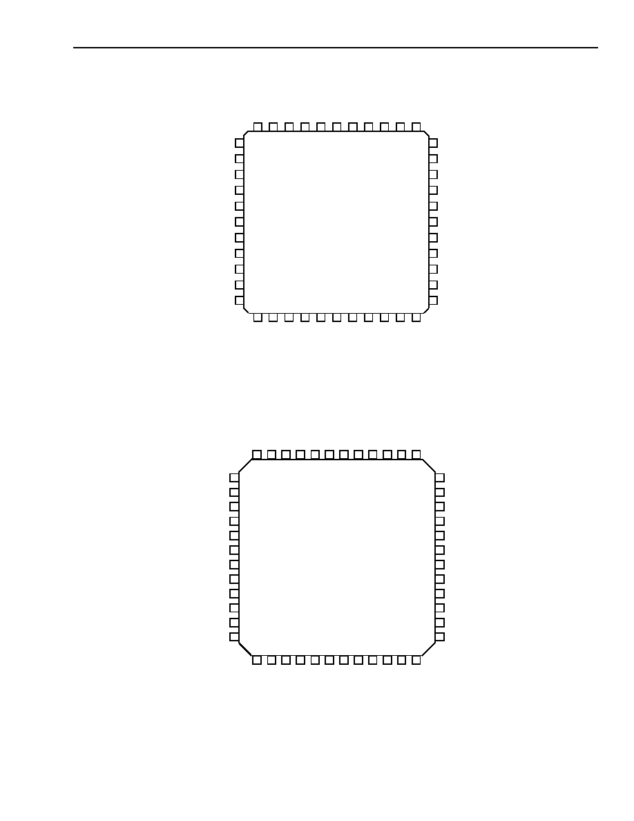
12 Outline Diagrams ...................................................................................................................................... 62
12.1
44-Pin EIAJ Quad Flat Pack (QFP) ................................................................................................ 62
12.2
48-Pin EIAJ Thin Quad Flat Pack (TQFP) ...................................................................................... 63

CSP1027 Voice Band Codec for
Data Sheet
Cellular Handset and Modem Applications
January 2002
Agere Systems Inc.
4
3 Pin Information
(continued)
Functional descriptions of the pins are found in Section 6 on page 30.
Table 1. Pin Descriptions
QFP Pin
TQFP Pin
Symbol
Type
Name/Function
1, 2, 3
1, 2, 3
RES
NC*
Reserved.
4
4
SMODE1
I
Serial Mode Select 1.
5
5
SMODE0
I
Serial Mode Select 0.
6, 7, 8,
9, 10
6, 7, 8,
9, 10, 11
RES
NC*
Reserved.
11
12
CKO1
O
Clock Output 1.
12
13
CLK
I
Clock Input.
13
14
XLO
I
Crystal Input.
14
15
XHI
O
Crystal Output.
15
16
XOSCEN
I
Crystal Oscillator Enable.
16
17
CKO2
O
Clock Output 2.
17
18
V
SS
P
Digital Ground.
18
19
SADD
I/O
Serial Address.
19
20
DI
I
Serial Input Data.
20
21
DO
O
Serial Output Data.
21
22
V
DD
P
Digital Power Supply.
--
23
RES
NC*
Reserved.
22
24
SYNC
I/O
Serial Input/Output Load Strobe and Synchronization.
23
25
IOCK
I
Serial
Clock.
24, 25,
26, 27, 28
26, 27, 28,
29, 30, 31
RES
NC*
Reserved.
29
32
RSTB
I
Reset.
30
33
PORB
O
Power-On Reset Output.
31
34
PORCAP
I
�
External Capacitor Connection for Power-On Reset.
32
35
SMODE2
I
Serial Mode Select 2.
33
36
EIGS
I
**
External Input Gain Select.
--
37
RES
NC*
Reserved.
34
38
V
SSA
P
Analog Ground.
35
39
V
REG
A
Regulated Output Voltage for Electrect Condenser Microphone.
36
40
V
DDA
P
Analog 5.0 V Power Supply.
37
41
AOUTN
A
Inverting Analog Output of Output Amplifier.
38
42
RES
NC*
Reserved.
39
43
AOUTP
A
Noninverting Analog Output of Output Amplifier.
40
44
V
SSA
P
Analog Ground.
41
45
MICIN
A
Analog Input for Microphone.
42
46
REFC
A
External Capacitor Connection for Internal Voltage Regulator.
43
47
AUXIN
A
Analog Input from Auxiliary.
44
48
V
DDA
P
Analog 5.0 V Power Supply.
*
Indicates no connection.
Indicates 3-state output.
Indicates pull-up device on input.
� Indicates pull-up resistor on input.
** Indicates pull-down device on input.