 | –≠–ª–µ–∫—Ç—Ä–æ–Ω–Ω—ã–π –∫–æ–º–ø–æ–Ω–µ–Ω—Ç: LCK4802 | –°–∫–∞—á–∞—Ç—å:  PDF PDF  ZIP ZIP |
Preliminary Data Sheet
July 2001
LCK4802
Low-Voltage PECL Differential Clock
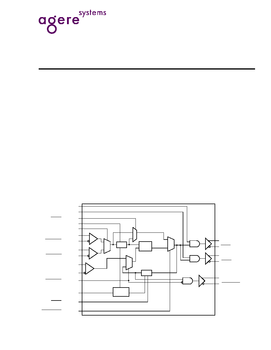
General
The LCK4802 is a low-voltage, 3.3 V PECL
differential clock synthesizer. The LCK4802 supports
two differential PECL output pairs with frequencies
from 336 MHz to 1 GHz. The clock is designed to
support single and multiple processor systems that
require PECL differential inputs. The LCK4802
contains a fully integrated PLL (phase-locked loop)
which multiplies the PECL_CLK input frequency to
match individual processor clock frequencies. The
PLL can be bypassed so that the PCLK outputs are
fed from the PECL_CLK or PECL_CLK input for test
purposes. All outputs are powered from a 2 V
external supply to reduce on-chip power
consumption. All outputs are PECL. The PLL can
operate in the internal feedback mode, or in the
external feedback mode for board level debugging
applications.
Features
s
Two fully selectable clock inputs.
s
Fully integrated PLL.
s
336 MHz to 1 GHz output frequencies.
s
PECL outputs.
s
PECL reference clock.
s
32-pin TQFP package.
Description
2274.b (F)
Figure 1. LCK4802 Logic Diagram
PCLK0_EN (PULL-UP)
PCLK1_EN (PULL-UP)
TESTM (PULL-UP)
PLLREF_EN (PULL-UP)
REF_SEL (PULL-UP)
PECL_CLK (PULL-UP)
PECL_CLK (PULL-UP)
EXTFB_IN (PECL)
(PULL-UP)
(PULL-DOWN)
EXTFB_EN (PULL-UP)
SEL[4:0] (PULL-UP)
RESET (PULL-UP)
PLL_BYPASS (PULL-UP)
EXTFB_OUT (PECL)
PCLK0
PCLK1
PLL
/N
/M
DECODE
0
1
0
1
1
0
0
1
PCLK0 (PECL)
PCLK1 (PECL)
EXTFB_OUT
PECL_CLK (PULL-UP)
PECL_CLK (PULL-UP)

2
Agere Systems Inc.
Preliminary Data Sheet
July 2001
Low-Voltage PECL Differential Clock
LCK4802
Description
(continued)
2275 (F)
Figure 2. 32-Pin TQFP
V
SS
RESET
SEL[4]
SEL[3]
SEL[2]
SEL[1]
SEL[0]
V
DDA
25
26
27
28
29
30
31
32
16
15
14
13
12
11
10
9
24
17
23
22
21
20
19
18
1
8
2
3
4
5
6
7
EXTFB_OUT
EXTFB_OUT
V
DDPECL
EXTFB_IN
EXTFB_IN
EXTFB_EN
PECL_CLK
PECL_CLK
PL
L
_
BYPASS
PL
L
R
EF_
E
N
V
D
D
PEC
L
PCL
K
0
PCL
K
0
PCL
K
1
PCL
K
1
V
D
D
PEC
L
V
DDD
TEST
M
V
SS
P
C
LK
0_
E
N
P
C
LK
1_
E
N
REF
_
S
E
L
PECL
_
CL
K
PECL
_
CL
K
Agere Systems Inc.
3
Preliminary Data Sheet
July 2001
Low-Voltage PECL Differential Clock
LCK4802
Pin Information
Table 1. Pin Description
Pin Number
Pin Name
I/O
1
Type
Description
1
V
DDD
P
Power Supply
3.3 V power supply.
2
TESTM
I
LVCMOS
M divider test pins.
3
V
SS
G
Ground
Digital ground.
4
PCLK0_EN
I
LVCMOS
PCLK0 enable.
5
PCLK1_EN
I
LVCMOS
PCLK1 enable.
6
REF_SEL
I
LVCMOS
Selects the PLL input reference clock.
7
PECL_CLK
I
Differential PECL
PLL reference clock input.
8
PECL_CLK
I
Differential PECL
PLL reference clock input.
9
PECL_CLK
I
Differential LVPECL PLL reference clock input.
10
PECL_CLK
I
Differential LVPECL PLL reference clock input.
11
EXTFB_EN
I
LVCMOS
External feedback enable.
12
EXTFB_IN
I
Differential PECL
External feedback input.
13
EXTFB_IN
I
Differential PECL
External feedback input.
14
V
DDPECL
P
Power Supply
Output buffers power supply.
15
EXTFB_OUT
O
Differential PECL
External feedback output clock.
16
EXTFB_OUT
O
Differential PECL
External feedback output clock.
17
V
DDPECL
P
Power Supply
Output buffers power supply.
18
PCLK1
O
Differential PECL
Output clock 1.
19
PCLK1
O
Differential PECL
Output clock 1.
20
PCLK0
O
Differential PECL
Output clock 0.
21
PCLK0
O
Differential PECL
Output clock 0.
22
V
DDPECL
P
Power Supply
Output buffers power supply.
23
PLLREF_EN
I
LVCMOS
PLL reference enable.
24
PLL_BYPASS
I
LVCMOS
Input signal PLL bypass.
25
V
SS
P
Ground
Analog ground for PLL.
26
RESET
I
LVCMOS
PLL bypass reset (for test use).
27
SEL[4]
I
LVCMOS
Selection of input and feedback frequency.
28
SEL[3]
I
LVCMOS
Selection of input and feedback frequency.
29
SEL[2]
I
LVCMOS
Selection of input and feedback frequency.
30
SEL[1]
I
LVCMOS
Selection of input and feedback frequency.
31
SEL[0]
I
LVCMOS
Selection of input and feedback frequency.
32
V
DDA
P
Power Supply
3.3 V filtered for PLL (PLL power supply).
1. P = power, I = input, G = ground, O = output.

4
Agere Systems Inc.
Preliminary Data Sheet
July 2001
Low-Voltage PECL Differential Clock
LCK4802
Pin Information
(continued)
Table 2. Frequency Selection
Selection
Input
Divide
Feedback
Divide
PCLK (MHz)
for Given Input Frequency (MHz)
4
3
2
1
0
M
N
70
100
120
125
0
0
0
0
0
5
24
336
480
576
600
0
0
0
0
1
5
25
350
500
600
625
0
0
0
1
0
5
26
364
520
624
650
0
0
0
1
1
5
27
378
540
648
675
0
0
1
0
0
5
28
392
560
672
700
0
0
1
0
1
5
29
406
580
696
725
0
0
1
1
0
5
30
420
600
720
750
0
0
1
1
1
5
31
434
620
744
775
0
1
0
0
0
5
32
448
640
768
800
0
1
0
0
1
5
33
462
660
792
825
0
1
0
1
0
5
34
476
680
816
850
0
1
0
1
1
5
35
490
700
840
875
0
1
1
0
0
5
36
504
720
864
900
0
1
1
0
1
5
37
518
740
888
925
0
1
1
1
0
5
38
532
760
912
950
0
1
1
1
1
5
39
546
780
936
975
1
0
0
0
0
5
40
560
800
960
1000
1
0
0
0
1
5
41
564
820
984
NA
1
0
0
1
0
5
42
588
840
NA
NA
1
0
0
1
1
5
43
602
860
NA
NA
1
0
1
0
0
5
44
616
880
NA
NA
1
0
1
0
1
5
45
630
900
NA
NA
1
0
1
1
0
5
46
644
920
NA
NA
1
0
1
1
1
5
47
658
940
NA
NA
1
1
0
0
0
5
48
672
960
NA
NA
1
1
0
0
1
5
49
686
980
NA
NA
1
1
0
1
0
5
50
700
1000
NA
NA
1
1
0
1
1
5
51
714
NA
NA
NA
1
1
1
0
0
5
52
728
NA
NA
NA
1
1
1
0
1
5
53
742
NA
NA
NA
1
1
1
1
0
5
54
756
NA
NA
NA
1
1
1
1
1
5
55
770
NA
NA
NA

Agere Systems Inc.
5
Preliminary Data Sheet
July 2001
Low-Voltage PECL Differential Clock
LCK4802
Pin Information
(continued)
Table 3. Function Control
Absolute Maximum Characteristics
Stresses in excess of the absolute maximum ratings can cause permanent damage to the device. These are
absolute stress ratings only. Functional operation of the device is not implied at these or any other conditions in
excess of those given in the operational sections of the data sheet. Exposure to absolute maximum ratings for
extended periods can adversely affect device reliability.
Table 4. Absolute Maximum Ratings
Control Pin
0
1
REF_SEL
PECL_CLK.
PECL_CLK.
TESTM
M divider test mode enabled.
Reference fed to bypass MUX.
PLLREF_EN
Disable the input to the PLL and reset
the M divider.
Enable the input to the PLL.
PLL_BYPASS
Outputs fed by input reference or M
divider.
Outputs fed by VCO.
EXTFB_EN
External feedback enabled.
Internal feedback enabled.
PCLK0_EN
PCLK0 = low, PCLK0 = high.
PCLK0 = high, PCLK0 = low.
PCLK1_EN
PCLK1 = low, PCLK1 = high.
PCLK1 = high, PCLK1 = low.
RESET
Resets feedback N divider.
Feedback enabled.
SEL[4:0]
See Table 2 on page 4.
See Table 2 on page 4.
Parameter
Symbol
Min
Typical
Max
Unit
Power Supply
V
DDD
/V
DDA
≠0.5
--
4.4
V
V
DDPECL
≠0.5
--
4.4
Input Voltage
V
IN
≠0.5
--
V
DDD
+ 0.3
V
Write Current
I
IN
≠1
--
1
mA
Storage Temperature
T
S
≠50
--
150
∞C

6
Agere Systems Inc.
Preliminary Data Sheet
July 2001
Low-Voltage PECL Differential Clock
LCK4802
Electrical Characteristics
Table 5. dc Characteristics
V
DDA
= V
DDD
= 3.3 V ± 5%, V
DDPECL
= 1.7 V--2.1 V, T
A
= 0 ∞C--70 ∞C.
Symbol
Description
Min
Typ
Max
Unit
Condition
V
IH
Input High Voltage
2.2
--
2.4
V
LVCMOS
V
IL
Input Low Voltage
1.5
--
1.8
V
LVCMOS
V
CMR
Input High Voltage
1
1. dc levels will vary 1:1 with V
DDD
.
V
DDD
≠ 1.3
--
V
DDD
≠ 0.5
V
LVPECL
V
PP
Input Low Voltage
1
0.5
--
--
V
LVPECL
V
OH
Output High Voltage
2.0
--
2.6
V
PECL
V
OL
Output Low Voltage
1.3
--
1.9
V
PECL
I
DDI
Core Supply Current
--
--
140
mA
--
I
DDA
PLL Supply Current
--
15
20
mA
--
I
DDO
Output Supply Current
--
150
--
mA
--
2
2. Two PCLK signals to 25
, and one EXTFB signal through 50
.
Theta
JA
Junction to Ambient
Thermal Resistance
--
53
--
∞C/W
--
3
3. 1.3 M/s (250 fpm) airflow.
Agere Systems Inc.
7
Preliminary Data Sheet
July 2001
Low-Voltage PECL Differential Clock
LCK4802
Electrical Characteristics
(continued)
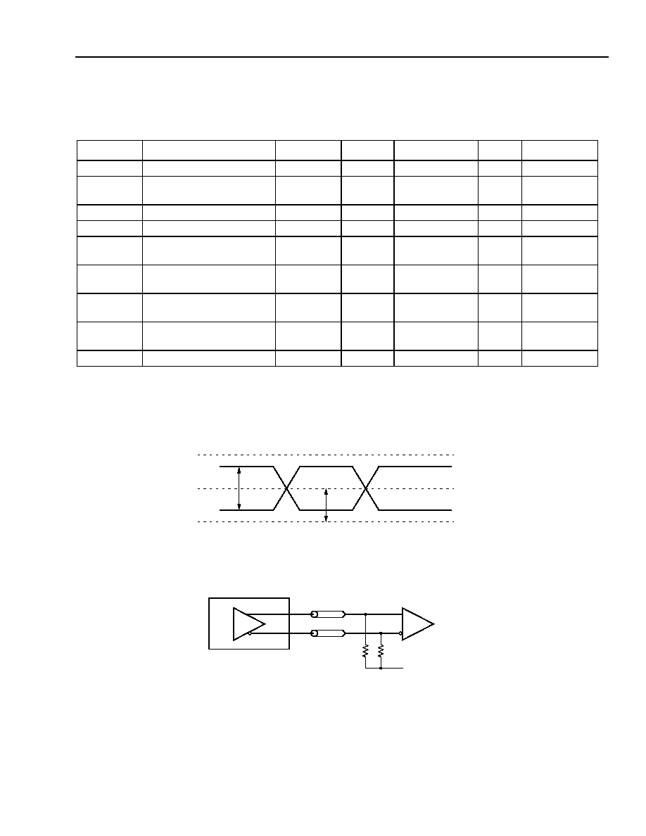
Table 6. ac Characteristics
V
DDA
= V
DDD
= 3.3 V ± 5%, V
DDPECL
= 1.7 V--2.1 V, T
A
= 0 ∞C--70 ∞C.
2276 (F)
Figure 3. PECL Differential Input Levels
2277.a (F)
Figure 4. Output Termination and ac Test Reference
Symbol
Description
Min
Typ
Max
Unit
Condition
fref
Input Frequency
--
70--125
--
MHz
--
fMAX
Maximum Output
Frequency
336
--
1000
MHZ
--
1
1. When the phase-locked loop is active but in bypass mode, fref maximum is limited by input the buffer; optimum performance is obtained
from PECL input.
tsk (o)
Skew Error (PCLK)
--
--
35
ps
--
2
2. At differential pair crossover.
t
jit (0)
Phase Jitter (I/O Jitter)
--
--
(output period)/2
--
--
2
t
jit (cc)
Cycle-to-Cycle Jitter
(Full Period)
--
--
5
%
--
2,
3
3. Full PCLK period.
t
jit (1/2 period)
Cycle-to-Cycle Jitter
(Half Period)
--
--
8
%
--
2,
4
4. Half PCLK period.
V
DIFout
Differential Output
Peak-to-Peak Swing
0.6
--
--
V
For all PECL
output pairs.
V
X
Differential Output
Crosspoint Voltage
0.68
--
0.9
V
For all PECL
output pairs.
t
lock
Maximum PLL Lock Time
--
--
10
ms
--
V
DIF
V
CM
V
DDPECL
V
OH
V
X
V
OL
V
SS
OUTPUT
Z = 50
V
TT
= V
SS
(GROUND)
R
T
= 25

8
Agere Systems Inc.
Preliminary Data Sheet
July 2001
Low-Voltage PECL Differential Clock
LCK4802
Applications
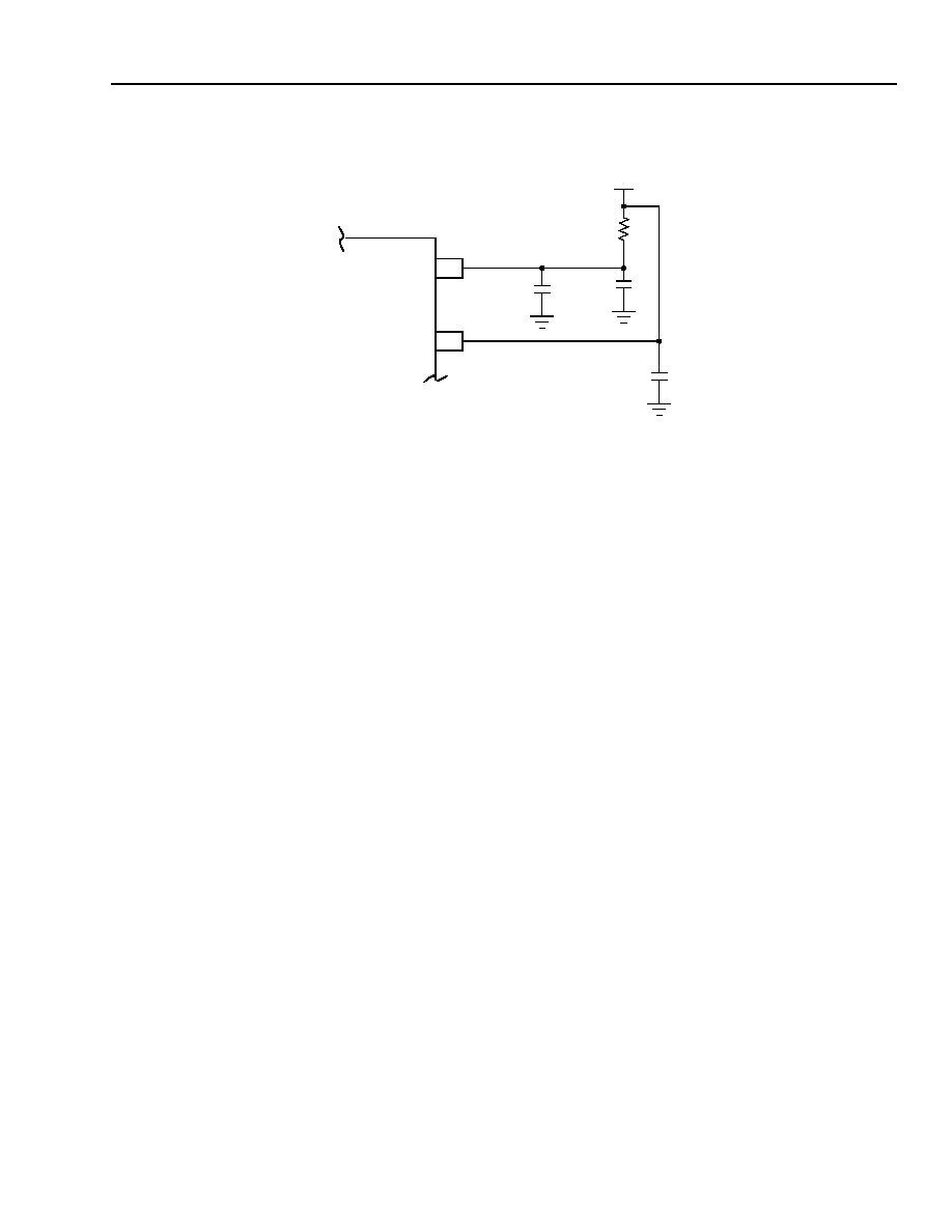
Power Supply Filtering
The LCK4802 is a mixed analog/digital product. Because of this, it exhibits some sensitivities that would not
necessarily be seen on a fully digital product. Analog circuitry is susceptible to random noise, the worst case being
when this noise is seen on the power supply pins. The LCK4802 provides separate power supplies for the output
buffers (V
DDPECL
) and the phase-locked loop (V
DDA
) of the device in order to isolate the high digital output
switching noise from the internal analog PLL. In a controlled evaluation board environment, this level of isolation is
adequate. However, in a digital system, a second level of isolation is suggested.
The easiest way to accomplish this is to add a power supply filter on the V
DDA
pin of the LCK4802. Figure 5 on
page 9 shows the typical power supply scheme. The filter should be designed in the 10 kHz--1 MHz range, since
this is the most likely frequency range to cause spectral content noise.
Note the dc voltage drop between V
DDD
and V
DDA
on the power supply filter. Very little dc voltage drop can be
tolerated when a 3.3 V V
DDD
supply is used. The power supply filter in Figure 5 must be 5
--10
in order to
meet the drop criteria. The RC filter in Figure 5 will provide a broadband filter with approximately 100:1 attenuation
above 20 kHz.
The impedance of an individual capacitor begins to appear inductive and increases with frequency as the noise
frequency crosses the series resonant point of the capacitor. The parallel capacitor combination ensures that for
frequencies much greater than the bandwidth of the PLL there is always a low-impedance path.
Agere Systems Inc.
9
Preliminary Data Sheet
July 2001
Low-Voltage PECL Differential Clock
LCK4802
Applications
(continued)
2278 (F)
Figure 5. Power Supply Filter
Although the LCK4802 has an isolated power supply and grounds, as well as fully differential PLL, there still may
be applications in which overall performance is being compromised due to system power supply noise. The power
supply filter schemes discussed are adequate to eliminate power supply noise problems in most designs.
R
S
= 5--10
V
DDA
V
DDD
0.01
µ
F
22
µ
F
3.3 V
0.01
µ
F
Preliminary Data Sheet
July 2001
Low-Voltage PECL Differential Clock
LCK4802
Agere Systems Inc. reserves the right to make changes to the product(s) or information contained herein without notice. No liability is assumed as a result of their use or application.
Copyright © 2001 Agere Systems Inc.
All Rights Reserved
Printed in U.S.A.
July 2001
DS01-265HSI
For additional information, contact your Agere Systems Account Manager or the following:
INTERNET:
http://www.agere.com
E-MAIL:
docmaster@micro.lucent.com
N. AMERICA: Agere Systems Inc., 555 Union Boulevard, Room 30L-15P-BA, Allentown, PA 18109-3286
1-800-372-2447, FAX 610-712-4106 (In CANADA: 1-800-553-2448, FAX 610-712-4106)
ASIA PACIFIC: Agere Systems Singapore Pte. Ltd., 77 Science Park Drive, #03-18 Cintech III, Singapore 118256
Tel. (65) 778 8833, FAX (65) 777 7495
CHINA:
Agere Systems (Shanghai) Co., Ltd., 33/F Jin Mao Tower, 88 Century Boulevard Pudong, Shanghai 200121 PRC
Tel. (86) 21 50471212, FAX (86) 21 50472266
JAPAN:
Agere Systems Japan Ltd., 7-18, Higashi-Gotanda 2-chome, Shinagawa-ku, Tokyo 141, Japan
Tel. (81) 3 5421 1600, FAX (81) 3 5421 1700
EUROPE:
Data Requests: DATALINE: Tel. (44) 7000 582 368, FAX (44) 1189 328 148
Technical Inquiries: GERMANY: (49) 89 95086 0 (Munich), UNITED KINGDOM: (44) 1344 865 900 (Ascot),
FRANCE: (33) 1 40 83 68 00 (Paris), SWEDEN: (46) 8 594 607 00 (Stockholm), FINLAND: (358) 9 3507670 (Helsinki),
ITALY: (39) 02 6608131 (Milan), SPAIN: (34) 1 807 1441 (Madrid)
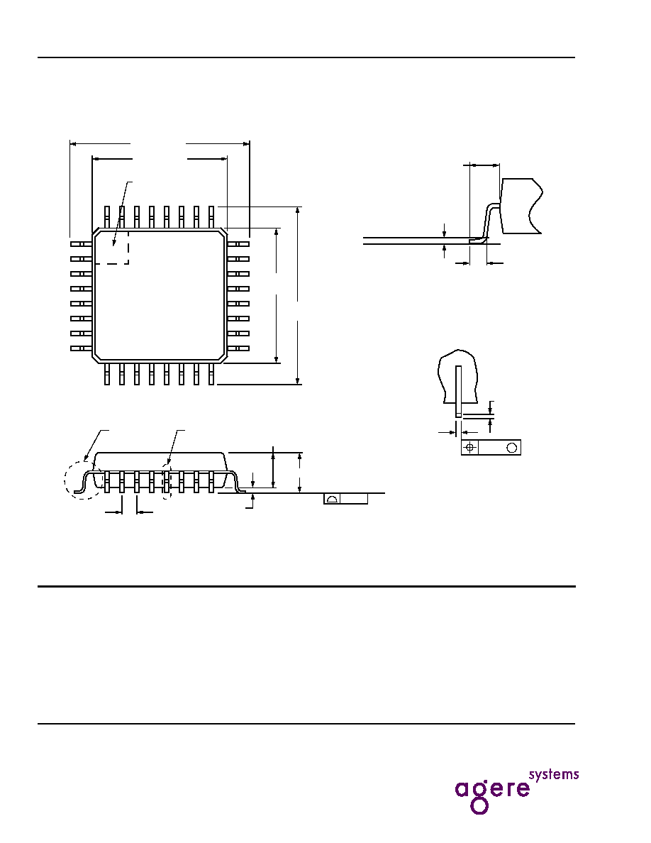
Outline Diagram
Dimensions are in millimeters.
12-3076(F)
PIN #1
IDENTIFIER ZONE
16
7.00 ± 0.20
9.00 ± 0.20
1
32
25
8
9
24
17
9.00
± 0.20
7.00
± 0.20
1.60 MAX
SEATING PLANE
DETAIL A
0.10
1.40 ± 0.05
0.80 TYP
0.05/0.15
DETAIL B
DETAIL B
0.30/0.45
0.20
M
0.09/0.200
DETAIL A
0.45/0.75
GAGE PLANE
SEATING PLANE
1.00 REF
0.25