 | –≠–ª–µ–∫—Ç—Ä–æ–Ω–Ω—ã–π –∫–æ–º–ø–æ–Ω–µ–Ω—Ç: LCK4950 | –°–∫–∞—á–∞—Ç—å:  PDF PDF  ZIP ZIP |

Data Sheet
November 2001
LCK4950
Low-Voltage PLL Clock Driver
Features
s
Fully integrated phase-locked loop (PLL)
s
Oscillator or crystal reference input
s
Output frequency up to 180 MHz
s
Outputs disable in high impedance
s
Compatible with PowerPC
Æ
, Intel
Æ
, and high-
performance RISC microprocessors
s
TQFP packaging
s
Output frequency configurable
s
±35 ps typical cycle-to-cycle jitter
s
Pin compatible with the Motorola
Æ
MPC950 clock
driver
Description
The LCK4950 is a PLL-based clock driver device
intended for high-performance clock tree designs.
The LCK4950 is 3.3 V compatible with output
frequencies of up to 180 MHz and output skews of
200 ps. The LCK4950 can accommodate the most
demanding tree designs by employing a fully
differential PLL design. This minimizes cycle-to-cycle
jitter, which is critical when the device is acting as the
reference clock for PLLs in today's microprocessors
and ASICs. The device has nine low-skew
configurable outputs for support of the clocking
needs of the various high-performance
microprocessors.
To provide input reference clock flexibility, two
selectable division ratios are available on the
LCK4950. The internal V
CO
runs at either 2x or 4x
the high-speed output. The FBSEL pin is used to
select between a divide by 8 or a divide by 16 of the
V
CO
frequency to be compared with the input
reference. These selections allow the input reference
to be either one-half, one-fourth, or one-eighth of the
high-speed output.
The LCK4950 is capable of scan clock distribution or
system diagnostics due to an external test clock
input. The REF_SEL pin allows the selection
between a crystal input to an on-chip oscillator for the
reference or selection of a TTL level oscillator input
directly. Only a parallel resonant crystal is required
for the onboard crystal oscillator external
components.
The LCK4950 is fully 3.3 V compatible and requires
no external loop filter components. All inputs accept
LVCMOS or LVTTL compatible levels while the
outputs provide LVCMOS levels with the capability to
drive terminated 50
transmission lines. The
LCK4950 can drive two traces, giving the device an
effective fan out of 1:18 for series-terminated 50
lines. For optimum performance and board density,
the device is packaged in a 7 mm x 7 mm 32-lead
TQFP package.

2
Agere Systems Inc.
Data Sheet
November 2001
Low-Voltage PLL Clock Driver
LCK4950
Description
(continued)
5-9698 (F)
Figure 1. Logic Diagram
fsela
PLL_En
Tclk
Ref_Sel
xtal1
xtal2
FBsel
(PULL-DOWN)
fselb
fselc
MR/OE
fseld
POWER-ON RESET
˜
4/
˜
8
˜
4/
˜
8
˜
4/
˜
8
˜
2/
˜
4
Qa
Qb
Qc0
Qc1
Qd0
Qd1
Qd2
Qd3
Qd4
(V
CO
)
200 MHz--480 MHz
PHASE
DETECTOR
LPF
˜
8/
˜
16
xtal
OSC

Agere Systems Inc.
3
Data Sheet
November 2001
Low-Voltage PLL Clock Driver
LCK4950
Pin Information
5-9699 (F)
Figure 2. Pin Diagram
Functional Description
Table 1. Function Tables
Ref_Sel
Function
1
TCLK
0
XTAL_OSC
PLL_En
Function
1
PLL Enabled
0
PLL Bypass
FBsel
Function
1
˜
8
0
˜
16
MR/OE
Function
1
Outputs Disabled
0
Outputs Enabled
fseln
Function
1
Qa =
˜
4; Qb:d =
˜
8
0
Qa =
˜
2; Qb:d =
˜
4
LCK4950
25
26
27
28
29
30
31
32
16
15
14
13
12
11
10
9
8
7
6
5
4
3
2
1
17
18
19
20
21
22
23
24
V
SS
Qb
V
DD
Qa
V
SS
TCLK
PLL_En
Ref_Sel
V
SS
Qd
1
V
DD
Qd
0
V
SS
Qc
1
V
DD
Qc
0
Qd2
V
DD
Qd3
V
SS
Qd4
V
DD
MR/OE
xtal2
xt
al
1
V
SS
fs
e
l
d
fs
e
l
c
fs
e
l
b
fs
e
l
a
FB
se
l
V
DDA

4
4
Agere Systems Inc.
Data Sheet
November 2001
Low-Voltage PLL Clock Driver
LCK4950
Functional Description
(continued)
Table 2. Function Table
Note: x = fVCO/4; 200 MHz < fVCO < 480 MHz.
Table 3. PLL Input Reference Characteristics
* Maximum and minimum input reference is limited by the V
CO
lock range and the feedback divider for the TCLK or xtal1 inputs.
See the Applications section for more crystal information.
Inputs
Outputs
Totals
fsela
fselb
fselc
fseld
Qa(1)
Qb(1)
Qc(2)
Qd(5)
Total 2x
Total x
Total x/2
0
0
0
0
2x
x
x
x
1
8
0
0
0
0
1
2x
x
x
x/2
1
3
5
0
0
1
0
2x
x
x/2
x
1
6
2
0
0
1
1
2x
x
x/2
x/2
1
1
7
0
1
0
0
2x
x/2
x
x
1
7
1
0
1
0
1
2x
x/2
x
x/2
1
2
6
0
1
1
0
2x
x/2
x/2
x
1
3
5
0
1
1
1
2x
x/2
x/2
x/2
1
0
8
1
0
0
0
x
x
x
x
0
9
0
1
0
0
1
x
x
x
x/2
0
4
5
1
0
1
0
x
x
x/2
x
0
7
2
1
0
1
1
x
x
x/2
x/2
0
2
7
1
1
0
0
x
x/2
x
x
0
8
1
1
1
0
1
x
x/2
x
x/2
0
3
6
1
1
1
0
x
x/2
x/2
x
0
6
3
1
1
1
1
x
x/2
x/2
x/2
0
1
8
Characteristic
Symbol
Min
Max
Unit
TCLK Input Rise/Falls
t
r
, t
f
--
3.0
ns
Reference Input Frequency
f
ref
--*
--*
MHz
Crystal Oscillator Frequency
f
Xtal
12.5
25
MHz
Reference Input Duty Cycle
f
refdc
25
75
%

Agere Systems Inc.
5
Data Sheet
November 2001
Low-Voltage PLL Clock Driver
LCK4950
Applications
Programming the LCK4950S
Several frequency relationships are configurable by the LCK4950. Frequency ratios of 1:1, 2:1, 4:1, and 4:2:1 are
possible from configuring the output dividers for the four output groups. To ensure that the output duty cycle is
always 50%, the LCK4950 uses even dividers. Table 4 illustrates output configurations of the LCK4950, describing
the outputs using the V
CO
frequency as a reference. For example, setting the Qa outputs to V
CO
/2, the Qb and Qc
to V
CO
/4, and the Qd to V
CO
/8 would provide the output frequency relationship of 4:2:1.
Table 4. Programmable Output Frequency Relationships
The division settings establish the output relationship, but one must still ensure that the V
CO
will be stable given the
frequency of the outputs desired. The feedback frequency should be used to situate the V
CO
into a frequency
range in which the PLL will be stable. The design of the PLL is such that for output frequencies between 25 MHz
and 180 MHz, the LCK4950 can generally be configured into a stable region.
Inputs
Outputs
FSELA
FSELB
FSELC
FSELD
Qa
Qb
Qc
Qd
0
0
0
0
V
CO
/2
V
CO
/4
V
CO
/4
V
CO
/4
0
0
0
1
V
CO
/2
V
CO
/4
V
CO
/4
V
CO
/8
0
0
1
0
V
CO
/2
V
CO
/4
V
CO
/8
V
CO
/4
0
0
1
1
V
CO
/2
V
CO
/4
V
CO
/8
V
CO
/8
0
1
0
0
V
CO
/2
V
CO
/8
V
CO
/4
V
CO
/4
0
1
0
1
V
CO
/2
V
CO
/8
V
CO
/4
V
CO
/8
0
1
1
0
V
CO
/2
V
CO
/8
V
CO
/8
V
CO
/4
0
1
1
1
V
CO
/2
V
CO
/8
V
CO
/8
V
CO
/8
1
0
0
0
V
CO
/4
V
CO
/4
V
CO
/4
V
CO
/4
1
0
0
1
V
CO
/4
V
CO
/4
V
CO
/4
V
CO
/8
1
0
1
0
V
CO
/4
V
CO
/4
V
CO
/8
V
CO
/4
1
0
1
1
V
CO
/4
V
CO
/4
V
CO
/8
V
CO
/8
1
1
0
0
V
CO
/4
V
CO
/8
V
CO
/4
V
CO
/4
1
1
0
1
V
CO
/4
V
CO
/8
V
CO
/4
V
CO
/8
1
1
1
0
V
CO
/4
V
CO
/8
V
CO
/8
V
CO
/4
1
1
1
1
V
CO
/4
V
CO
/8
V
CO
/8
V
CO
/8

6
6
Agere Systems Inc.
Data Sheet
November 2001
Low-Voltage PLL Clock Driver
LCK4950
Applications
(continued)
Table 5. Input Reference vs. Output Frequency Relationships
The relationship between the input reference and the output frequency is very flexible. Table 5 shows the
multiplication factors between the inputs and outputs for the LCK4950. Figure 3 through Figure 6 illustrate several
programming possibilities.
Note: The variations of the configurations shown are not complete, but do represent potential applications.
Config
fsela
fselb
fselc
fseld
FB_Sel = 1
FB_Sel = 0
Qa
Qb
Qc
Qd
Qa
Qb
Qc
Qd
1
0
0
0
0
4x
2x
2x
2x
8x
4x
4x
4x
2
0
0
0
1
4x
2x
2x
x
8x
4x
4x
2x
3
0
0
1
0
4x
2x
x
2x
8x
4x
2x
4x
4
0
0
1
1
4x
2x
x
x
8x
4x
2x
2x
5
0
1
0
0
4x
x
2x
2x
8x
2x
4x
4x
6
0
1
0
1
4x
x
2x
x
8x
2x
4x
2x
7
0
1
1
0
4x
x
x
2x
8x
2x
2x
4x
8
0
1
1
1
4x
x
x
x
8x
2x
2x
2x
9
1
0
0
0
2x
2x
2x
2x
4x
4x
4x
4x
10
1
0
0
1
2x
2x
2x
x
4x
4x
4x
2x
11
1
0
1
0
2x
2x
x
2x
4x
4x
2x
4x
12
1
0
1
1
2x
2x
x
x
4x
4x
2x
2x
13
1
1
0
0
2x
x
2x
2x
4x
2x
4x
4x
14
1
1
0
1
2x
x
2x
x
4x
2x
4x
2x
15
1
1
1
0
2x
x
x
2x
4x
2x
2x
4x
16
1
1
1
1
2x
x
x
x
4x
2x
2x
2x

Agere Systems Inc.
7
Data Sheet
November 2001
Low-Voltage PLL Clock Driver
LCK4950
Applications
(continued)
5-9700 (F)
Figure 3. Dual-Frequency Configuration
5-9701 (F)
Figure 4. Dual-Frequency Configuration
66.66 MHz
33.33 MHz
33.33 MHz
66.66 MHz
fsela
fselb
fselc
fseld
FBsel
Qd
Qc
Qb
Qa
INPUT REF
16.66 MHz
0
0
1
1
1
1
1
2
5
33.33 MHz
66.66 MHz
66.66 MHz
66.66 MHz
fsela
fselb
fselc
fseld
FBsel
Qd
Qc
Qb
Qa
INPUT REF
33.33 MHz
1
1
1
0
0
1
1
2
5
5-9702 (F)
Figure 5. Dual-Frequency Configuration
5-9703 (F)
Figure 6. Triple-Frequency Configuration
33.33 MHz
33.33 MHz
33.33 MHz
66.66 MHz
fsela
fselb
fselc
fseld
FBsel
Qd
Qc
Qb
Qa
INPUT REF
16.66 MHz
0
0
1
1
1
1
1
2
5
40 MHz
40 MHz
80 MHz
160 MHz
fsela
fselb
fselc
fseld
FBsel
Qd
Qc
Qb
Qa
INPUT REF
20 MHz
0
1
0
0
1
1
1
2
5
Absolute Maximum Ratings
Stresses in excess of the absolute maximum ratings can cause permanent damage to the device. These are
absolute stress ratings only. Functional operation of the device is not implied at these or any other conditions in
excess of those given in the operational sections of the data sheet. Exposure to absolute maximum ratings for
extended periods can adversely affect device reliability.
Table 6. Absolute Maximum Ratings
Parameter
Symbol
Min
Max
Unit
Supply Voltage
V
DD
, V
DDA
≠0.3
4.6
V
Input Voltage
V
I
≠0.3
V
DD
+ 0.3
V
Input Current
I
IN
--
±20
mA
Storage Temperature Range
T
Stor
≠40
125
∞C

8
8
Agere Systems Inc.
Data Sheet
November 2001
Low-Voltage PLL Clock Driver
LCK4950
Electrical Characteristics
Table 7. dc Characteristics
T
A
= 0 ∞C to 70 ∞C, V
CC
= 3.3 V ± 5%.
Table 8. ac Characteristics
T
A
= 0 ∞C to 70 ∞C, V
CC
= 3.3 V ± 5%.
Characteristic
Symbol
Min
Typ
Max
Unit
Condition
Input High Voltage (LVCMOS inputs)
V
IH
2.0
--
3.6
V
--
Input Low Voltage (LVCMOS inputs)
V
IL
--
--
0.8
V
--
Output High Voltage
V
OH
2.4
--
--
V
I
OH
=
≠40 mA
1
1. The LCK4950 outputs can drive series or parallel-terminated 50
(or 50
to V
CC
/2) transmission lines on the incident edge.
Output Low Voltage
V
OL
--
--
0.5
V
I
OL
= 40 mA
1
Input Current
I
IN
--
--
±120
µA
--
Input Capacitance
C
IN
--
--
4
pF
--
Power Dissipation Capacitance
C
pd
--
25
--
pF
Per Output
Maximum Quiescent Supply Current
Non-PLL
I
DDQ
--
--
1
mA
All V
DD
Pins
Except V
DDA
2
2. Total power = (I
DDPLL
+ I
DDQ
) x V + (fQaCQa + fQbCQb + fQc0CQc0 + fQc1CQc1 + fQd0CQd0 + fQd1CQd1 + fQd2CQd2 + fQd3CQd3 +
fQd4CQd4) x V
2
; where V = V
DD, CQa
= load capacitance on Qa, CQb = load capacitance on Qb, etc.
Maximum PLL Supply Current
I
DDPLL
--
--
55
mA
V
DDA
Pin Only
Characteristic
Symbol
Min
Typ
Max
Unit
Condition
Output Rise/Fall Time
t
r
, t
f
0.10
--
1.0
ns
0.8 V to 2.0 V
Output Duty Cycle
t
pw
48.5
--
52.5
%
--
Same Frequencies
Output-to-Output Skews
t
sk(0)
--
150
300
ps
--
Different Frequencies:
Qa
fmax
< 150 MHz
Qa
fmax
> 150 MHz
--
--
200
--
400
400
ps
ps
--
--
PLL V
CO
(feedback = V
CO
/4)
Lock (feedback = V
CO
/8)
Range (feedback = V
CO
/16)
f
VCO
200
200
200
--
--
--
480
480
480
MHz
MHz
MHz
--
--
--
Maximum Output Frequency:
Qa(
˜
2)
Qa/Qb (
˜
4)
Qb (
˜
8)
f
max
--
--
--
--
--
--
180
120
60
MHz
MHz
MHz
--
--
--
Output Disable Time
t
PLZ,HZ
--
--
7
ns
--
Output Enable Time
t
PZL
--
--
6
ns
--
Cycle-to-Cycle Jitter (peak-to-peak)
t
jitter
--
±35
±50
ps
--
1
1.See Applications section for more information.
Maximum PLL Clock Time
t
lock
--
--
10
ms
--

Agere Systems Inc.
9
Data Sheet
November 2001
Low-Voltage PLL Clock Driver
LCK4950
Electrical Characteristics
(continued)
Jitter Performance of the LCK4950S
More focus is given to clock distribution design and management today because of the continuing increase of
today's digital system's clock rates. System-clock jitter and its effect on overall system timing budget is at the
center of this focus. The LCK4950 is designed to utilize a differential CMOS PLL and incorporate multiple power
and ground pins in the design to minimize clock jitter. The following text provides details on the jitter performance,
illustrates measurement limitations, and provides guidelines to minimize the jitter of the LCK4950.
The most commonly specified jitter parameter is cycle-to-cycle jitter. With today's high-performance measurement
equipment, there is no way to measure this parameter for jitter performance in the class demonstrated by the
LCK4950. As a result, different methods are used which approximate cycle-to-cycle jitter. The typical method of
measuring the jitter is to accumulate a large number of cycles, create a histogram of the edge placements, and
record peak-to-peak as well as standard deviations of the jitter. It is of great importance to measure the edge
immediately following the trigger edge. If this is not the case, the measurement inaccuracy will add significantly to
the measured jitter. The oscilloscope cannot collect adjacent pulses. It is safe to assume that collecting pulse
information in this mode will produce jitter values somewhat larger than if consecutive cycles were measured;
therefore, this measurement will represent an upper bound of cycle-to-cycle jitter. Most likely, this is a conservative
estimate of the cycle-to-cycle jitter.
There are two common sources of jitter for a PLL-based clock driver. The most common source of jitter is random
jitter. Less commonly known is the jitter produced by different frequency outputs switching synchronously. If all of
the outputs are switching at the same frequency, the PLL jitter is equal to the total jitter of the device. In the
LCK4950, where a number of the outputs can be switching synchronously but at different frequencies, a
multimodal jitter distribution can be seen on the highest frequency outputs. It is important to consider what is
happening on the other outputs because the output being monitored is affected by the activity on the other outputs.
From Figure 7, one can see that for each rising edge on the higher-frequency signal, the activity on the lower-
frequency signal is not consistent.
The placement of the edge that is being monitored is displaced in time due to the activity on the other outputs
altering the internal thresholds of the device. The relationship is periodic because the signals are synchronous.
The resulting jitter is a superposition of the PLL jitter on the displaced edges. The multimodal distribution will
appear to be a fat Gaussian distribution, or a truly multimodal distribution depending on the size of the PLL jitter
and displacement of the edges. When all the outputs are switching at the same frequency, there is no edge
displacement and the jitter is that of the PLL.

10
10
Agere Systems Inc.
Data Sheet
November 2001
Low-Voltage PLL Clock Driver
LCK4950
Electrical Characteristics
(continued)
5-9704 (F)
Figure 7. PLL Jitter and Edge Displacement
1
2
2
1
1
2
2
3
1
2
3
1
2
PEAK-TO-PEAK PLL JITTER
PEAK-TO-PEAK PERIOD JITTER
PEAK-TO-PEAK PLL JITTER
PEAK-TO-PEAK PERIOD JITTER
1
2
3
Agere Systems Inc.
11
Data Sheet
November 2001
Low-Voltage PLL Clock Driver
LCK4950
Electrical Characteristics
(continued)
5-9707 (F)
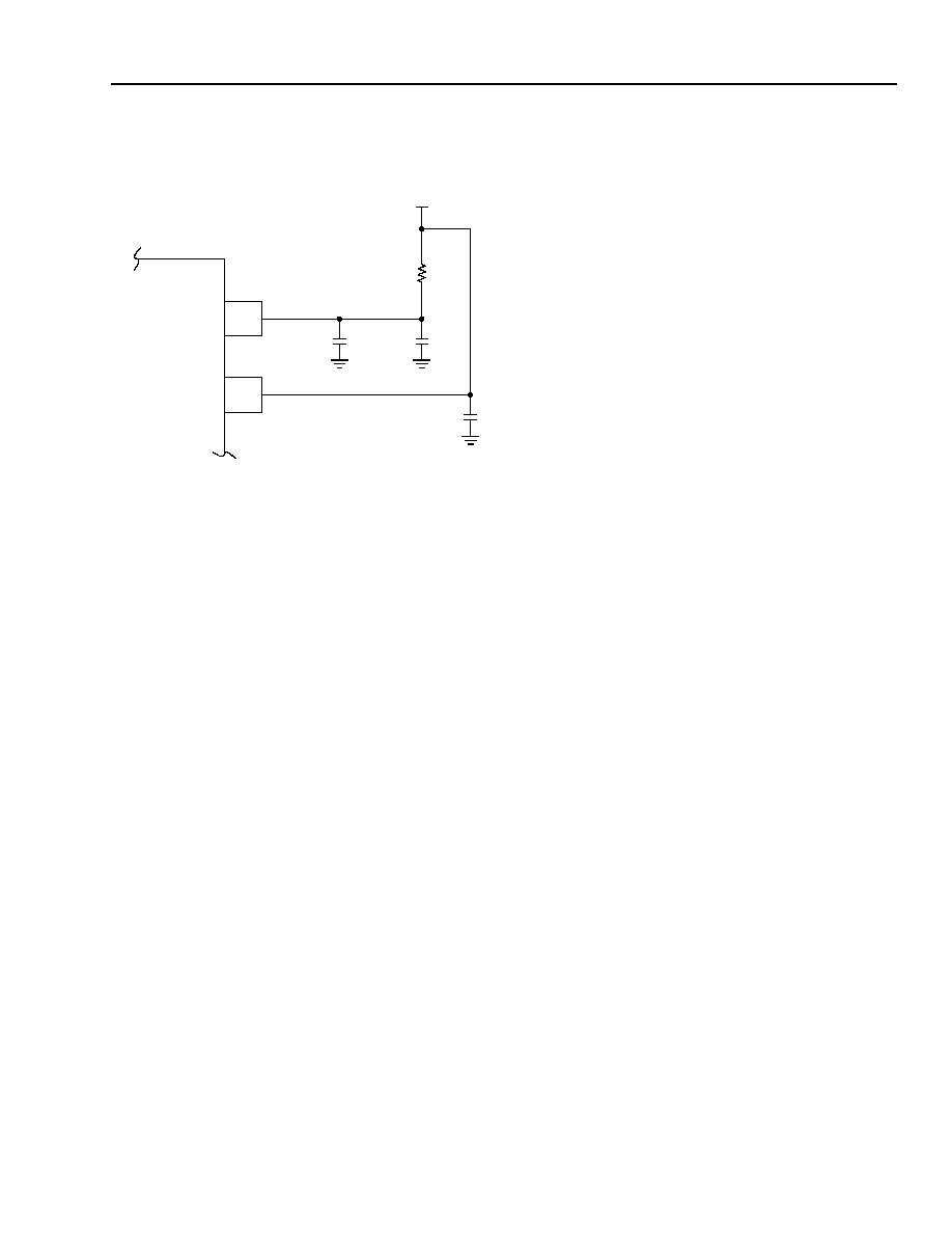
Figure 8. Power Supply Filter
PLL jitter can be measured for configurations where
the outputs are switching at different frequencies by
triggering the lowest-frequency output. PLL jitter is
dependent on internal V
CO
frequency more so than
output configuration.
There are some general guidelines that will minimize
the output jitter of the device. First, always configure
the device so the V
CO
runs as fast as possible. This is
the most important aspect in minimizing jitter of the
LCK4950. Second, maintain the reference frequency at
the highest possible frequency. These more frequent
phase detector updates help to reduce jitter. There is a
trade-off between higher reference frequencies and
higher V
CO
frequency; always choose a higher V
CO
frequency to reduce jitter. Third, and the most difficult
to follow, minimize the number of different frequencies
sourced from a single chip. The fixed edge
displacement associated with the switching noise, in
most cases, nearly doubles the effective jitter of a high-
speed output.
Power Supply Filtering
The LCK4950 exhibits some sensitivities that would not
be seen on a fully digital product because the LCK4950
is a mixed analog/digital product. Analog circuitry is
naturally sensitive to random noise, most noticeably
when the noise is in the power supply pins. The
LCK4950 provides a separate output buffer power
supply (V
DD
) and phase-locked loop (V
DDA
) power
supply pins. This design isolates the high
switching noise digital outputs from the sensitive
internal analog phase-locked loop. In a controlled
setup (i.e., an evaluation board), this amount of
isolation will suffice. In a digital system, where it is
much more difficult to minimize noise on the power
supplies, an additional level of isolation may be
required. The easiest means of accomplishing this is
by applying a power supply filter on the V
DDA
pin for
the LCK4950.
Figure 8 illustrates a typical power supply filter scheme
for the LCK4950. The device is most greatly affected
by spectral content in the 1 kHz to 1 MHz range, and
therefore needs a filter to target this range. The most
important aspect of this final filter design is the dc
voltage drop between the V
DD
supply and V
DDA
pin.
The I
DDPLL
current (current forced through the V
DDA
pin) is normally 45 mA (55 mA maximum), assuming
that a minimum of 3.0 V must be maintained on the
V
DDA
pin. Very little voltage drop can be tolerated when
a 3.3 V V
DD
supply is used. The resistor shown in
Figure 10 must have a resistance of 5
--10
to meet
the voltage drop criteria. The RC filter shown provides
a broadband filter with about 100:1 attenuation for
noise, with a spectral content above 20 kHz. As the
noise frequency crosses the series resonant point of an
individual capacitor, its overall impedance begins to
look inductive and therefore increases with increasing
frequency. The parallel capacitor circuit shown in
Figure 11 guarantees that a low- impedance path to
ground exists for frequencies exceeding the bandwidth
of the PLL. It is recommended that the user start with
an 8
--10
resistor to avoid potential V
DD
drop
problems and only use higher-value resistors when a
higher level of attenuation is needed.
The LCK4950 has several design features to minimize
the susceptibility to power supply noise (isolated power
and grounds and fully differential PLL). Still, there may
be applications in which overall performance is being
degraded due to system power supply noise. The
power supply filter schemes discussed in this section
should be adequate to eliminate power supply noise-
related problems in most designs.
0.01
µ
F
22
µ
F
R
S
=
5
--10
V
CC
PLL_V
CC
LCK4950
0.01
µ
F
3.3 V

12
Agere Systems Inc.
Data Sheet
November 2001
Low-Voltage PLL Clock Driver
LCK4950
Electrical Characteristics
(continued)
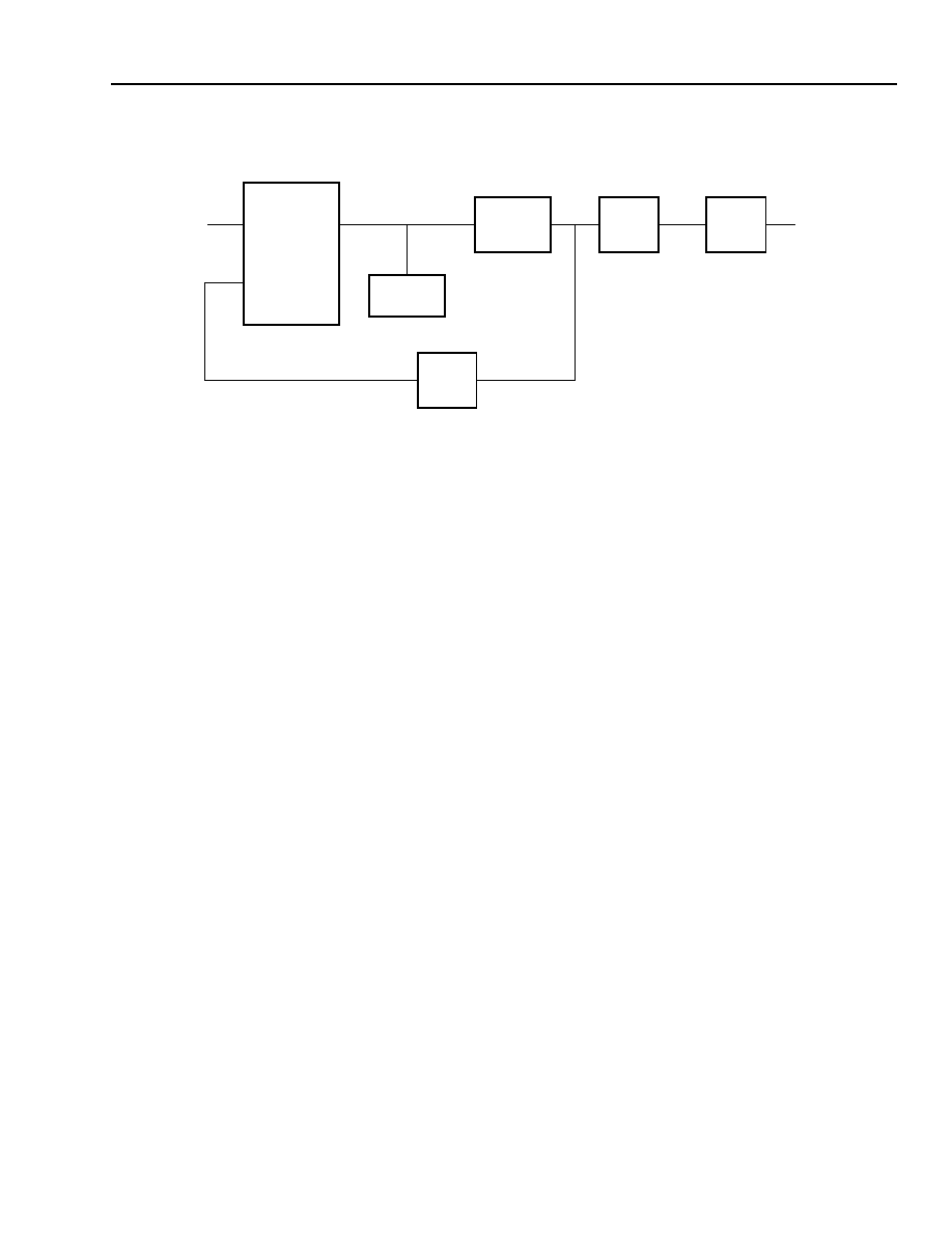
Using the On-Chip Crystal Oscillator
The LCK4950 features an on-chip crystal oscillator buffer to allow for seed clock generation as well as final
distribution. The only external component required is the crystal since the on-chip oscillator buffer is completely
self-contained. The user is advised to mount the crystal as close to the LCK4950 as possible to avoid board-level
parasitics since the oscillator is, to a degree, sensitive to loading at the inputs. To facilitate collocation, surface-
mount crystals are recommended, but not required.
The oscillator circuit is a parallel resonant circuit with on-chip shunt capacitors. A parallel resonant crystal is simply
a crystal that has been characterized in its parallel resonant mode. Therefore, in the majority of cases, a parallel
specified crystal or a series resonant crystal can be used with the LCK4950 with just a minor frequency error.
Typically, a series crystal used in a parallel resonant mode will exhibit an oscillatory frequency a few hundred ppm
different than the specified value. For most processor implementations, a few hundred ppm translates into kHz
inaccuracies, a small enough level not to represent a major issue.
The LCK4950 is a clock driver that was designed to generate outputs with programmable frequency relationships.
As a result, the crystal input frequency is a function of the desired output frequency. To determine the crystal
required to produce the desired output frequency for an application that utilizes internal feedback, the PLL block
diagram (Figure 9) should be used. The P and the M values for the LCK4950 are also included in Figure 9. The M
values can be found in Table 1 on page 3.
Table 9. Crystal Specifications
Parameter
Value
Crystal Cut
Fundamental AT Cut
Resonance
Parallel Resonance
Frequency Tolerance
±75 ppm at 25 ∞C
Frequency/Temperature Stability
±150 ppm at 0
∞C to 70 ∞C
Operating Range
0
∞C to 70 ∞C
Shunt Capacitors
10 pF--40 pF
Equivalent Series Resistance (ESR)
50
to 80
Max
Correction Drive Level
100 µW
Aging
5 ppm/yr (first three years)
Agere Systems Inc.
13
Data Sheet
November 2001
Low-Voltage PLL Clock Driver
LCK4950
Electrical Characteristics
(continued)
5-9708 (F)
Figure 9. PLL Block Diagram
Note: For computations refer to the following equations:
m = 8 (FBsel = 1), 16(FBsel = 0), P = 1
For the LCK4950 clock driver, the following will provide an example of how to determine the crystal frequency
required for a given design.
Given:
Qa = 160 MHz
Qb = 80 MHz
Qc = 40 MHz
Qd = 40 MHz
FBSel = 0
(eq. 1)
From Figure 3:
fQd = V
CO
/8 then N = 8 or fQa = V
CO
/2 then N = 2
From Figure 9:
m = 16 and P = 1
or
PHASE
DETECTOR
LPF
V
CO
˜
P
˜
N
˜
m
Qn
f
ref
f
f
VCO
m
--------------
f
vco
fQ
=
,
=
f
ref
fQn
N
P
∑
∑
m
------------------------------
=
f
ref
fQn
N
P
∑
∑
m
------------------------------
=
t
ref
40
8
1
∑
∑
16
------------------------
20 MHz
=
=
t
ref
160
2
1
∑
∑
16
----------------------------
20 MHz
=
=

14
Agere Systems Inc.
Data Sheet
November 2001
Low-Voltage PLL Clock Driver
LCK4950
Electrical Characteristics
(continued)
Driving Transmission Lines
The LCK4950 clock driver was designed to drive high-speed signals in a terminated transmission line environment.
The output drivers were designed to exhibit the lowest impedance possible to provide the optimum flexibility to the
user. With an output impedance of less than 10
,
the drivers can drive either parallel-terminated or series-
terminated transmission lines.
Point-to-point distribution of signals is the method of choice in most high-performance clock networks. In a point-to-
point scheme, either series-terminated or parallel-terminated transmission lines can be used. The parallel
technique terminates the signal at the end of the line with a 50
resistance to V
DD
/2. Only a single terminated line
can be driven by each output of the LCK4950 clock driver because this technique draws a fairly high level of dc
current. For the series driven case, however, there is no dc current draw and the outputs can drive multiple series-
terminated lines. Figure 10 illustrates an output driving a single series-terminated line.
5-9709 (F)
Figure 10. Single Transmission Line
The situation in Figure 11 should be used to better match the impedances when driving multiple lines. In this case,
the series-terminating resistors are reduced so when the parallel combination is added to the output buffer
impedance the line impedance is perfectly matched.
5-9710 (F)
Figure 11. Optimized Dual Line Termination
IN
OUTPUT
7
BUFFER
R
S
= 43
Z
O
= 50
OutA
OUTPUT
7
BUFFER
R
S
= 36
Z
O
= 50
R
S
= 36
Z
O
= 50

Agere Systems Inc.
15
Data Sheet
November 2001
Low-Voltage PLL Clock Driver
LCK4950
Outline Diagram
Dimensions are in millimeters.
12-3076(F)
PIN #1
IDENTIFIER ZONE
16
7.00 ± 0.20
9.00 ± 0.20
1
32
25
8
9
24
17
9.00
± 0.20
7.00
± 0.20
1.60 MAX
SEATING PLANE
DETAIL A
0.10
1.40 ± 0.05
0.80 TYP
0.05/0.15
DETAIL B
DETAIL B
0.30/0.45
0.20
M
0.09/0.200
DETAIL A
0.45/0.75
GAGE PLANE
SEATING PLANE
1.00 REF
0.25

PowerPC is a registered trademark of International Business Machines Corporation.
Intel is a registered trademark of Intel Corporation.
Motorola is a registerd trademark of Motorola, Inc.
Copyright © 2001 Agere Systems Inc.
All Rights Reserved
November 2001
DS02-033HSI (Replaces DS01-118ANET)
Agere Systems Inc. reserves the right to make changes to the product(s) or information contained herein without notice. No liability is assumed as a result of their use or application.
For additional information, contact your Agere Systems Account Manager or the following:
INTERNET:
http://www.agere.com
E-MAIL:
docmaster@agere.com
N. AMERICA:
Agere Systems Inc., 555 Union Boulevard, Room 30L-15P-BA, Allentown, PA 18109-3286
1-800-372-2447, FAX 610-712-4106 (In CANADA: 1-800-553-2448, FAX 610-712-4106)
ASIA:
Agere Systems Hong Kong Ltd., Suites 3201 & 3210-12, 32/F, Tower 2, The Gateway, Harbour City, Kowloon
Tel. (852) 3129-2000, FAX (852) 3129-2020
CHINA: (86) 21-5047-1212 (Shanghai), (86) 10-6522-5566 (Beijing), (86) 755-695-7224 (Shenzhen)
JAPAN: (81) 3-5421-1600 (Tokyo), KOREA: (82) 2-767-1850 (Seoul), SINGAPORE: (65) 778-8833, TAIWAN: (886) 2-2725-5858 (Taipei)
EUROPE:
Tel. (44) 7000 624624, FAX (44) 1344 488 045