 | –≠–ª–µ–∫—Ç—Ä–æ–Ω–Ω—ã–π –∫–æ–º–ø–æ–Ω–µ–Ω—Ç: OR3TP12 | –°–∫–∞—á–∞—Ç—å:  PDF PDF  ZIP ZIP |
Document Outline
- Introduction
- PCI Bus Core Highlights
- FPSC Highlights
- Software Support
- Description
- OR3TP12 Overview
- PCI Bus Core Detailed Description
- PCI Bus Core Master Controller Detailed Description
- PCI Bus Core Target Controller Detailed Description
- FPGA Configuration Target Controller Data Format
- Bit Stream Error Checking
- FPGA Configuration Modes
- Absolute Maximum Ratings
- Recommended Operating Conditions
- Electrical Characteristics
- Timing Characteristics
- Input/Output Buffer Measurement Conditions
- Output Buffer Characteristics
- Estimating Power Dissipation
- Pin Information
- Package Thermal Characteristics Summary
- Package Thermal Characteristics
- Package Coplanarity
- Package Parasitics
- Package Outline Diagrams
- Ordering Information
- List of Tables
- Table 1 . PCI Local Bus Data Rates
- Table 2 . ORCA PCI FPSC SolutionsÑAvailable FPGA Resources
- Table 3 . PCI Bus Command Descriptions
- Table 4 . Timing Budgets
- Table 5 . PCI Bus Pin Descriptions
- Table 6 . Embedded Core/FPGA Interface Signals
- Table 7 . OR3TP12 FPGA/PCI Core Interface Signal Locations
- Table 8 . PCI Bus Core Options Settable via FPGA Configuration RAM Bits
- Table 9 . Index to State Sequence Tables
- Table 10 . Bit Definitions for Master Command/Address Phase
- Table 11 . Holding Registers, Examples of Typical Operation
- Table 12 . Master State Counter (MStateCntr) Values and the Corresponding Bus Data
- Table 13 . Dual-Port Master Writes
- Table 14 . Quad-Port Master Writes
- Table 15 . Dual-Port Master Read, Specified Burst Length
- Table 16 . Quad-Port Master Read, Duplicate Burst Length
- Table 17 . Quad-Port Master Read, Specified Burst Length
- Table 18 . Bit Destinations for Target Command/Address Phase
- Table 19 . Target State Counter (TStateCntr) Values and the Corresponding Bus Data
- Table 20 . Dual-Port Target Write
- Table 21 . Quad-Port Target Write
- Table 22 . Dual-Port Target Read
- Table 23 . Quad-Port Target Read
- Table 24 . Configuration Space Layout
- Table 25 . Configuration Space Assignment
- Table 26 . Configuration Frame Format and Contents
- Table 27 . Configuration Frame Size
- Table 28 . Configuration Modes
- Table 29 . Absolute Maximum Ratings
- Table 30 . Recommend Operating Conditions
- Table 31 . Electrical Characteristics
- Table 32 . Derating for Commercial Devices (I/O Supply VDD)
- Table 33 . OR3TP12 PCI and FPGA Interface Clock Operation Frequencies
- Table 34 . OR3TP12 FPGA to PCI, and PCI to FPGA, Combinatorial Path Delays
- Table 35 . OR3TP12 FPGA Side Interface Combinatorial Path Delay Signals
- Table 36 . OR3TP12 Interbuf Delays
- Table 37 . OR3TP12 FPGA Side Interface Clock to Output Delays, pciclk Synchronous Signals
- Table 38 . OR3TP12 FPGA Side Interface Clock to Output Delays, fclk Synchronous Signals
- Table 39 . OR3TP12 FPGA Side Interface Input Setup Delays, pciclk Synchronous Signals
- Table 40 . OR3TP12 FPGA Side Interface Input Setup Delays, fclk Synchronous Signals
- Table 41 . FPGA Common-Function Pin Descriptions
- Table 42 . OR3TP12 240-Pin SQFP2 Pinout
- Table 43 . OR3TP12 256-Pin PBGA Pinout
- Table 44 . OR3TP12 352-Pin PBGA Pinout
- Table 45 . ORCA OR3TP12 Plastic Package Thermal Guidelines
- Table 46 . ORCA OR3TP12 Package Parasitics
- Table 47 . Voltage Options
- Table 48 . Temperature Options
- Table 49 . Package Options
- Table 50 . ORCA Series 3+ Package Matrix
- Table 51 . Embedded Core Type
- Table 52 . FPSC Base Array
- List of Figures
- Figure 1 . OR3TP12 Array
- Figure 2 . ORCA OR3TP12 PCI FPSC Block Diagram
- Figure 3 . Master Write Single (FIFO Interface, Dual-Port)
- Figure 4 . Master Write Single (FIFO Interface, Quad-Port)
- Figure 5 . Master Write Single (PCI Bus, 32-Bit)
- Figure 6 . Master Write Burst (FIFO Interface, Dual-Port)
- Figure 7 . Master Write Burst (FIFO Interface, Quad-Port)
- Figure 8 . Master Write Burst (PCI Bus, 32-Bit)
- Figure 9 . Master Read Single (FIFO Interface, Dual-Port)
- Figure 10 . Master Read Single (FIFO Interface, Quad-Port)
- Figure 11 . Master Read Single (PCI Bus, 32-Bit)
- Figure 12 . Master Read Burst (FIFO Interface, Dual-Port)
- Figure 13 . Master Read Burst (FIFO Interface, Quad-Port)
- Figure 14 . Master Read Burst (PCI Bus, 32-Bit)
- Figure 15 . Target Configuration Write (PCI Bus, 32-Bit)
- Figure 16 . Target I/O Write, Nondelayed (PCI Bus, 32-Bit)
- Figure 17 . Target Memory Single Write (PCI Bus, 32-Bit)
- Figure 18 . Target Write Single (FIFO Interface, Dual-Port)
- Figure 19 . Target Write Single (FIFO Interface, Quad-Port)
- Figure 20 . Target Memory Write Burst (PCI Bus, 32-Bit)
- Figure 21 . Target Write Burst (FIFO Interface, Dual-Port)
- Figure 22 . Target Write Burst (FIFO Interface, Quad-Port)
- Figure 23 . Target Configuration Read (PCI Bus, 32-Bit)
- Figure 24 . Target I/O Read, Delayed (PCI Bus, 32-Bit)
- Figure 25 . Target I/O Read, Nondelayed (PCI Bus, 32-Bit)
- Figure 26 . Target Single Memory Read, Delayed (PCI Bus, 32-Bit)
- Figure 27 . Target Read Single (FIFO Interface, Dual-Port)
- Figure 28 . Target Read Single (FIFO Interface, Quad-Port)
- Figure 29 . Target Memory Read Single, Nondelayed Transaction (PCI Bus, 32-Bit)
- Figure 30 . Target Burst Memory Read, Delayed (PCI Bus, 32-Bit)
- Figure 31 . Target Read Burst (FIFO Interface, Dual-Port)
- Figure 32 . Target Read Burst (FIFO Interface, Quad-Port)
- Figure 33 . Target Memory Burst Read, Nondelayed (PCI Bus, 32-Bit)
- Figure 34 . FPSC Block Diagram and Clock Network
- Figure 35 . Serial Configuration Data FormatÑAutoincrement Mode
- Figure 36 . Serial Configuration Data FormatÑExplicit Mode
- Figure 37 . ac Test Loads
- Figure 38 . Output Buffer Delays
- Figure 39 . Input Buffer Delays
- Figure 40 . Sinklim (TJ = 25 ∞C, VDD = 3.3 V)
- Figure 41 . Slewlim (TJ = 25 ∞C, VDD = 3.3 V)
- Figure 42 . Fast (TJ = 25 ∞C, VDD = 3.3 V)
- Figure 43 . Sinklim (TJ = 125 ∞C, VDD = 3.0 V)
- Figure 44 . Slewlim (TJ = 125 ∞C, VDD = 3.0 V)
- Figure 45 . Fast (TJ = 125 ∞C, VDD = 3.0 V)
- Figure 46 . Package Parasitics
- Contact Us

Data Sheet
March 2000
ORCA
Æ
OR3TP12 Field-Programmable System Chip (FPSC)
Embedded Master/Target PCI Interface
Introduction
Lucent Technologies Microelectronics Group has
developed a solution for designers who need the
many advantages of an FPGA-based design imple-
mentation coupled with the high bandwidth of the
industry-standard PCI interface. The
ORCA
OR3TP12 FPSC provides a full-featured
33/50/66 MHz, 32-/64-bit PCI interface, fully
designed and tested, in hardware, plus FPGA logic
for user-programmable functions.
PCI Local Bus
PCI local bus, or simply, PCI bus, has become an
industry-standard interface protocol for use in appli-
cations ranging from desktop PC busing to high-
bandwidth backplanes in networking and communi-
cations equipment. The PCI bus specification* pro-
vides for both 5 V and 3.3 V signaling environments.
The PCI interface clock speed is specified in the
range from dc to 66 MHz with detailed specifications
at 33 MHz and 66 MHz as well as recommendations
for 50 MHz operation. Data paths are defined as
either 32-bit or 64-bit. These data path and frequency
combinations allow for the peak data transfer rates
described in Table 1.
Table 1. PCI Local Bus Data Rates
The PCI bus is electrically specified so that no glue
logic is required to interface to the bus--PCI devices
interface directly to the PCI bus. Other features
include registers for device and subsystem identifica-
tion and autoconfiguration, support for 64-bit
addressing, and multimaster capability that allows
any PCI bus Master access to any PCI bus Target.
PCI Bus Core Highlights
s
Implemented in an
ORCA
Series 3 base array, dis-
placing the bottom four rows of 18 columns.
s
Core is a well-tested ASIC model.
s
Fully compliant to Revision 2.1 of PCI Local Bus
Specification (and designed for Revision 2.2).
* PCI Local Bus Specification Rev. 2.1, PCI SIG, June 1, 1995.
Clock
Frequency
(MHz)
Data Path
Width (bits)
Peak Data Rate
(Mbytes)
33
32
132
33
64
264
66
32
264
66
64
528
Table 2.
ORCA
PCI FPSC Solutions--Available FPGA Resources
* The embedded core and interface comprise approximately 85K standard-cell ASIC gates in addition to these usable gates. The usable
gate counts range from a logic-only gate count to a gate count assuming 30% of the PFUs/SLICs being used as RAMs. The logic-only
gate count includes each PFU/SLIC (counted as 108 gates per PFU/SLIC), including 12 gates per LUT/FF pair (eight per PFU), and 12
gates per SLIC/FF pair (one per PFU). Each of the four PIOs per PIC is counted as 16 gates (two FFs, fast-capture latch, output logic, clk
drivers, and I/O buffers). PFUs used as RAM are counted at four gates per bit, with each PFU capable of implementing a 32
◊
4 RAM (or
512 gates) per PFU.
Device
Usable Gates
*
Number of
LUTs
Number of
Registers
Max User
RAM
Max User
I/Os
Array
Size
Number of
PFUs
OR3TP12
30K--60K
2016
2636
32K
187
14
◊
18
252

Table of Contents
Contents
Page
Contents
Page
ORCA OR3TP12 FPSC
Data Sheet
Embedded Master/Target PCI Interface
March 2000
2
Lucent Technologies Inc.
Introduction............................................................... 1
PCI Local Bus........................................................ 1
PCI Bus Core Highlights........................................... 1
FPSC Highlights ....................................................... 6
Software Support...................................................... 6
Description................................................................ 7
What Is an FPSC?................................................. 7
FPSC Overview..................................................... 7
FPSC Gate Counting............................................. 7
FPGA/Embedded Core Interface .......................... 7
FPSC Design Kit ................................................... 8
ORCA
Foundry Development System................... 8
FPGA Logic Overview ........................................... 8
PLC Logic.............................................................. 9
PIC Logic............................................................... 9
System Features ................................................... 9
Routing ..................................................................10
Configuration .........................................................10
More Series 3 Information .....................................10
OR3TP12 Overview..................................................10
Device Layout........................................................10
OR3TP12 PCI Bus Core Overview...........................10
PCI Bus Interface ..................................................10
Embedded Core Options/FPGA Configuration......12
PCI Bus Core Detailed Description ..........................13
PCI Bus Commands..............................................13
PCI Protocol Fundamentals ..................................16
PCI Bus Pin Information ........................................18
Embedded Core/FPGA Interface
Signal Descriptions ............................................21
Embedded Core/FPGA Interface
Signal Locations.................................................29
Embedded Core Configuration Options ................31
Embedded Core/FPGA FIFO Interface
Operation Summary ...........................................33
PCI Bus Core Master Controller
Detailed Description ..............................................34
FIFO Interface Overview .......................................34
Master Write Operation .........................................35
Master Read Operation .........................................43
PCI Bus Core Target Controller
Detailed Description .............................................. 53
Target FIFO Interface............................................ 53
Target Write Operation.......................................... 53
Target Read Operation.......................................... 65
Clocking Options at FPGA/Embedded
Core Boundary ...................................................80
Configuration Space of the PCI Bus Core.............82
FPSC Configuration ..............................................86
FPGA Configuration Target Controller
Data Format ..........................................................88
Using
ORCA
Foundry to Generate
Configuration RAM Data ....................................88
FPGA Configuration Data Frame ..........................88
Bit Stream Error Checking ........................................90
FPGA Configuration Modes......................................90
Absolute Maximum Ratings......................................91
Recommended Operating Conditions ......................91
Electrical Characteristics ..........................................92
Timing Characteristics ..............................................93
Description................................................................93
PFU Timing .......................................................... 94
PLC Timing........................................................... 94
SLIC Timing.......................................................... 94
PIO Timing ........................................................... 94
Special Function Timing ........................................94
Clock Timing .............................................................94
Configuration Timing .............................................94
Readback Timing ................................................. 94
Input/Output Buffer Measurement Conditions ..........99
Output Buffer Characteristics ................................. 100
Estimating Power Dissipation ................................. 101
Pin Information ....................................................... 102
JA
...................................................................... 119
JC
...................................................................... 119
JC
...................................................................... 119
JB
...................................................................... 119
FPGA Maximum Junction Temperature .............. 119
Package Thermal Characteristics........................... 120
Package Coplanarity .............................................. 120
Package Parasitics ................................................. 120
Package Outline Diagrams..................................... 122
Terms and Definitions ......................................... 122
240-Pin SQFP2 ................................................... 123
256-Pin PBGA ..................................................... 124
352-Pin PBGA ..................................................... 125
Ordering Information............................................... 126

Lucent Technologies Inc.
3
Data Sheet
ORCA OR3TP12 FPSC
March 2000
Embedded Master/Target PCI Interface
List of Figures
Figures
Page
Figures
Page
Figure 1. OR3TP12 Array....................................... 11
Figure 2.
ORCA
OR3TP12 PCI FPSC
Block Diagram ..................................................... 12
Figure 3. Master Write Single
(FIFO Interface, Dual-Port) .................................. 39
Figure 4. Master Write Single
(FIFO Interface, Quad-Port)................................. 40
Figure 5. Master Write Single
(PCI Bus, 32-Bit).................................................. 40
Figure 6. Master Write Burst
(FIFO Interface, Dual-Port) .................................. 41
Figure 7. Master Write Burst
(FIFO Interface, Quad-Port)................................. 42
Figure 8. Master Write Burst
(PCI Bus, 32-Bit).................................................. 42
Figure 9. Master Read Single
(FIFO Interface, Dual-Port) .................................. 46
Figure 10. Master Read Single
(FIFO Interface, Quad-Port)................................. 47
Figure 11. Master Read Single
(PCI Bus, 32-Bit).................................................. 47
Figure 12. Master Read Burst
(FIFO Interface, Dual-Port) .................................. 49
Figure 13. Master Read Burst
(FIFO Interface, Quad-Port)................................. 50
Figure 14. Master Read Burst
(PCI Bus, 32-Bit).................................................. 51
Figure 15. Target Configuration Write
(PCI Bus, 32-Bit).................................................. 57
Figure 16. Target I/O Write, Nondelayed
(PCI Bus, 32-Bit).................................................. 58
Figure 17. Target Memory Single Write
(PCI Bus, 32-Bit).................................................. 59
Figure 18. Target Write Single
(FIFO Interface, Dual-Port) .................................. 60
Figure 19. Target Write Single
(FIFO Interface, Quad-Port)................................. 61
Figure 20. Target Memory Write Burst
(PCI Bus, 32-Bit).................................................. 62
Figure 21. Target Write Burst
(FIFO Interface, Dual-Port) .................................. 63
Figure 22. Target Write Burst
(FIFO Interface, Quad-Port) ...................................64
Figure 23. Target Configuration Read
(PCI Bus, 32-Bit) ....................................................68
Figure 24. Target I/O Read, Delayed
(PCI Bus, 32-Bit) ....................................................69
Figure 25. Target I/O Read, Nondelayed
(PCI Bus, 32-Bit) ....................................................70
Figure 26. Target Single Memory Read,
Delayed (PCI Bus, 32-Bit) ......................................71
Figure 27. Target Read Single
(FIFO Interface, Dual-Port) ....................................72
Figure 28. Target Read Single
(FIFO Interface, Quad-Port) ...................................73
Figure 29. Target Memory Read Single,
Nondelayed Transaction (PCI Bus, 32-Bit).............74
Figure 30. Target Burst Memory Read,
Delayed (PCI Bus, 32-Bit) ......................................75
Figure 31. Target Read Burst
(FIFO Interface, Dual-Port) ....................................76
Figure 32. Target Read Burst
(FIFO Interface, Quad-Port) ...................................77
Figure 33. Target Memory Burst Read,
Nondelayed (PCI Bus, 32-Bit) ................................78
Figure 34. FPSC Block Diagram and
Clock Network........................................................81
Figure 35. Serial Configuration Data Format--
Autoincrement Mode ..............................................89
Figure 36. Serial Configuration Data Format--
Explicit Mode .........................................................89
Figure 37. ac Test Loads ..........................................99
Figure 38. Output Buffer Delays ...............................99
Figure 39. Input Buffer Delays ..................................99
Figure 40. Sinklim (T
J
= 25 ∞C, V
DD
= 3.3 V).......... 100
Figure 41. Slewlim (T
J
= 25 ∞C, V
DD
= 3.3 V) ......... 100
Figure 42. Fast (T
J
= 25 ∞C, V
DD
= 3.3 V) .............. 100
Figure 43. Sinklim (T
J
= 125 ∞C, V
DD
= 3.0 V)........100
Figure 44. Slewlim (T
J
= 125 ∞C, V
DD
= 3.0 V) ....... 100
Figure 45. Fast (T
J
= 125 ∞C, V
DD
= 3.0 V) ............ 100
Figure 46. Package Parasitics ................................ 121

Tables
Page
Tables
Page
ORCA OR3TP12 FPSC
Data Sheet
Embedded Master/Target PCI Interface
March 2000
4
Lucent Technologies Inc.
List of Tables
Table 1. PCI Local Bus Data Rates ...........................1
Table 2.
ORCA
PCI FPSC Solutions--
Available FPGA Resources ..................................1
Table 3. PCI Bus Command Descriptions ...............13
Table 4. Timing Budgets ..........................................17
Table 5. PCI Bus Pin Descriptions ...........................18
Table 6. Embedded Core/FPGA
Interface Signals ................................................21
Table 7. OR3TP12 FPGA/PCI Core
Interface Signal Locations..................................29
Table 8. PCI Bus Core Options Settable
via FPGA Configuration RAM Bits ....................31
Table 9. Index to State Sequence Tables.................33
Table 10. Bit Definitions for Master
Command/Address Phase .................................35
Table 11. Holding Registers,
Examples of Typical Operation...........................36
Table 12. Master State Counter (MStateCntr)
Values and the Corresponding Bus Data ...........36
Table 13. Dual-Port Master Writes...........................43
Table 14. Quad-Port Master Writes .........................43
Table 15. Dual-Port Master Read,
Specified Burst Length .......................................51
Table 16. Quad-Port Master Read,
Duplicate Burst Length.......................................52
Table 17. Quad-Port Master Read,
Specified Burst Length .......................................52
Table 18. Bit Destinations for Target
Command/Address Phase .................................54
Table 19. Target State Counter (TStateCntr)
Values and the Corresponding Bus Data ...........55
Table 20. Dual-Port Target Write..............................64
Table 21. Quad-Port Target Write ............................65
Table 22. Dual-Port Target Read .............................79
Table 23. Quad-Port Target Read ............................79
Table 24. Configuration Space Layout .....................82
Table 25. Configuration Space Assignment.............83
Table 26. Configuration Frame
Format and Contents .........................................89
Table 27. Configuration Frame Size.........................90
Table 28. Configuration Modes ................................90
Table 29. Absolute Maximum Ratings .....................91
Table 30. Recommend Operating Conditions ..........91
Table 31. Electrical Characteristics..........................92
Table 32. Derating for Commercial Devices
(I/O Supply V
DD
) ................................................93
Table 33. OR3TP12 PCI and FPGA Interface
Clock Operation Frequencies .............................95
Table 34. OR3TP12 FPGA to PCI, and PCI to
FPGA, Combinatorial Path Delays .....................95
Table 35. OR3TP12 FPGA Side Interface
Combinatorial Path Delay Signals......................96
Table 36. OR3TP12 Interbuf Delays ........................96
Table 37. OR3TP12 FPGA Side Interface Clock to
Output Delays, pciclk Synchronous Signals.......97
Table 38. OR3TP12 FPGA Side Interface Clock to
Output Delays, fclk Synchronous Signals ..........97
Table 39. OR3TP12 FPGA Side Interface Input
Setup Delays, pciclk Synchronous Signals ........98
Table 40. OR3TP12 FPGA Side Interface Input
Setup Delays, fclk Synchronous Signals............98
Table 41. FPGA Common-Function
Pin Descriptions ...............................................102
Table 42. OR3TP12 240-Pin SQFP2 Pinout..........105
Table 43. OR3TP12 256-Pin PBGA Pinout............109
Table 44. OR3TP12 352-Pin PBGA Pinout............113
Table 45.
ORCA
OR3TP12 Plastic Package
Thermal Guidelines..........................................120
Table 46.
ORCA
OR3TP12 Package Parasitics.....121
Table 47. Voltage Options ......................................126
Table 48. Temperature Options..............................126
Table 49. Package Options ....................................126
Table 50.
ORCA
Series 3+ Package Matrix ...........126
Table 51. Embedded Core Type.............................126
Table 52. FPSC Base Array ...................................126

Lucent Technologies Inc.
5
Data Sheet
ORCA OR3TP12 FPSC
March 2000
Embedded Master/Target PCI Interface
Lucent Technologies Inc.
PCI Bus Core Highlights
(continued)
s
Operates at PCI bus speeds up to 66 MHz.
s
Comprises two independent controllers for Master
and Target.
s
Meets/exceeds all requirements for
PICMG
*
Hot
Swap Friendly silicon, Full Hot Swap model, per the
CompactPCI
*
Hot Swap Specification,
PICMG
2.1
R1.0.
s
PCI SIG Hot-Plug (R1.0) compliant.
s
Four internal FIFOs individually buffer both directions
of both the Master and Target interfaces:
-- Both Master FIFOs are 64 bits wide by 32 bits
deep.
-- Both Target FIFOs are 64 bits wide by 16 bits
deep.
s
Capable of no-wait-state, full-burst PCI transfers in
either direction, on either the Master or Target inter-
face. Dual 32-bit data paths extend into the FPGA
logic, permitting full-bandwidth, simultaneous bidirec-
tional data transfers of up to 264 Mbytes/s to be sus-
tained indefinitely.
s
Can be configured to provide either two 32-bit buses
(one in each direction) to be multiplexed between
Master and Target, or four independent 16-bit buses.
s
Provides many hardware options in the PCI bus core
that are set during FPGA logic configuration.
s
Operates within the requirements of the PCI 5 V and
3.3 V signaling environments, allowing the same
device to be used in 5 V or 3.3 V PCI systems.
s
FPGA is reconfigurable via the PCI interface configu-
ration space (as well as conventionally), allowing the
FPGA to be field-updated to meet late-breaking
requirements of emerging protocols.
s
Master:
-- Generates all defined command codes except
interrupt acknowledge and special cycle.
-- Capable of acting as the system's configuration
agent by booting up with the Master logic enabled.
-- Provides multiple options to increase PCI bus
bandwidth.
s
Target:
-- Responds legally to most command codes: inter-
rupt acknowledge, special cycle, and reserved
commands ignored; memory read multiple and
line handled as memory read; memory write and
invalidate handled as memory write.
-- Implements Target abort, disconnect, retry, and
wait cycles.
-- Handles delayed transactions.
-- Handles fast back-to-back transactions.
-- Supports programmable latency timer control.
-- Method of handling wait-states is programmable
to allow tailoring to different Target data access
latencies.
-- Decodes at medium speed.
s
Supports dual-address cycles (both as Master and
Target).
s
Supports all six base address registers (BARs), as
either memory (32-bit or 64-bit) or I/O. Any legal
page size can be independently specified for each
BAR during FPGA configuration.
s
Provides versatile clocking capabilities with FPGA
clocks sourced from PCI bus clock or elsewhere.
FIFO interface buffers asynchronous clock domains
between the PCI interface and FPGA-based logic.
s
PCI interface timing: meets or exceeds 33 MHz,
50 MHz, and 66 MHz PCI requirements.
s
Standard 256-byte PCI configuration space:
-- Class code, revision ID.
-- Latency timer.
-- Cache line size.
-- Subsystem ID.
-- Subsystem vendor ID.
-- Maximum latency, minimum grant.
-- Interrupt line.
-- Hot plug/hot swap capability.
*
CompactPCI
and
PICMG
are registered trademarks of the PCI
Industrial Computer Manufacturers Group.
Parameter
33 MHz
50 MHz
66 MHz
Device clock = > out
11.0 ns
7.5 ns
6.0 ns
Device setup time
7.0 ns
4.5 ns
3.0 ns
Board prop. delay
10.0 ns
6.5 ns
5.0 ns
Board clock skew
2.0 ns
1.5 ns
1.0 ns
Total budget
30.0 ns
20.0 ns
15.0 ns

ORCA OR3TP12 FPSC
Data Sheet
Embedded Master/Target PCI Interface
March 2000
6
Lucent Technologies Inc.
Lucent Technologies Inc.
PCI Bus Core Highlights
(continued)
s
Generates interrupts on intan as directed by the
FPGA.
s
Provisions for 64-bit PCI bus capability in 352-pin
PBGA package.
s
Automatically detects 5 V or 3.3 V PCI bus signaling
environment and provides appropriate I/O signal
clamping.
s
Pinout compatible with the
ORCA
PCI Master/Target
Customer Solution Core V2.0 for OR2C/TxxA or
ORCA
Series 3 FPGAs.
s
Ideally suited for such applications as:
-- PCI-based graphics/video/multimedia.
-- Bridges to ISA/EISA/MCA, LAN, SCSI, Ethernet,
ATM, or other bus architectures.
-- High-bandwidth data transfer in proprietary sys-
tems.
FPSC Highlights
s
Implemented as an embedded core into the
advanced Series 3+
ORCA
FPSC architecture.
s
Allows the user to integrate the core with up to 60K
gates of programmable logic, all in one device, and
provides up to 187 user I/O pins in addition to the
PCI interface pins.
s
FPGA portion retains all of the features of the
ORCA
Series 3 FPGA architecture:
-- High-performance, cost-effective, 0.3 µm
4-level metal technology, with a migration plan to
0.25 µm technology.
-- Twin-quad programmable function unit (PFU)
architecture with eight 16-bit look-up tables
(LUTs) per PFU, organized in two nibbles for use
in nibble- or byte-wide functions. Allows for mixed
arithmetic and logic functions in a single PFU.
-- Softwired LUTs (SWL) allow fast cascading of up
to three levels of LUT logic in a single PFU for up
to 40% speed improvement (-5 speed grade).
-- Supplemental logic and interconnect cell (SLIC)
provides 3-statable buffers, up to 10-bit decoder,
and
PAL
*-like AND-OR-INVERT (AOI) in each
programmable logic cell (PLC).
-- Up to three ExpressCLK inputs allow extremely
fast clocking of signals on- and off-chip plus
access to internal general clock routing.
-- Dual-use microprocessor interface (MPI) can be
used for configuration, readback, device control,
and device status, as well as for a general-pur-
pose interface to the FPGA. Glueless interface to
i960
and
PowerPC
processors with user-config-
urable address space provided.
-- Programmable clock manager (PCM) adjusts
clock phase and duty cycle for input clock rates
from 5 MHz to 120 MHz. The PCM may be com-
bined with FPGA logic to create complex func-
tions, such as digital phase-locked loops (DPLL),
frequency counters, and frequency synthesizers
or clock doublers. Two PCMs are provided per-
device.
-- True internal 3-state, bidirectional buses with sim-
ple control provided by the SLIC.
-- 32
◊
4 RAM per PFU, configurable as single or
dual-port at >170 MHz (-5 speed). Create large,
fast RAM/ROM blocks (128
◊
8 in only eight
PFUs) using the SLIC decoders as bank drivers.
-- Built-in boundary scan (
IEEE
ß
1149.1 JTAG) and
TS_ALL testability function to 3-state all I/O pins.
s
High-speed on-chip interface provided between
FPGA logic and embedded core to reduce bottle-
necks typically found when interfacing off-chip.
s
Supported in three packages: 240-pin SQFP2,
256-pin PBGA, and 352-pin PBGA (64-bit PCI in
352-pin PBGA only).
Software Support
s
Supported by
ORCA
Foundry software and third-
party CAE tools for implementing
ORCA
Series 3+
devices and simulation/timing analysis with embed-
ded PCI bus core.
s
PCI bus core configuration options and simulation
models generated by FPSC configuration manager
utility in
ORCA
FPSC Design Kit software.
s
Timing constraints provided for interface between
PCI bus core and FPGA logic.
*
PAL
is a trademark of Advanced Micro Devices, Inc.
i960
is a registered trademark of Intel Corporation.
PowerPC
is a registered trademark of International Business
Machines Corporation.
ß
IEEE
is a registered trademark of The Institute of Electrical and
Electronics Engineers, Inc.

Lucent Technologies Inc.
7
Data Sheet
ORCA OR3TP12 FPSC
March 2000
Embedded Master/Target PCI Interface
Lucent Technologies Inc.
Description
What Is an FPSC?
FPSCs, or field-programmable system chips, are
devices that combine field-programmable logic with
ASIC or mask-programmed logic on a single device.
FPSCs provide the time to market and flexibility of
FPGAs, the design effort savings of using soft intellec-
tual property (IP) cores, and the speed, design density,
and economy of ASICs.
FPSC Overview
Lucent's Series 3+ FPSCs are created from Series 3
ORCA
FPGAs. To create a Series 3+ FPSC, several
rows of programmable logic cells (see FPGA Logic
Overview section for FPGA logic details) are removed
from a Series 3
ORCA
FPGA, and the area is replaced
with an embedded logic core. Other than replacing
some FPGA gates with ASIC gates, at greater than
10:1 efficiency, none of the FPGA functionality is
changed--all of the Series 3 FPGA capability is
retained: MPI, PCMs, boundary scan, etc. The rows of
programmable logic are replaced at the bottom of the
device, allowing pins on the bottom and sides of the
replaced rows to be used as I/O pins for the embedded
core. The remainder of the device pins retain their
FPGA functionality as do special function FPGA pins
within the embedded core area.
The embedded cores can take many forms and gener-
ally come from Lucent Technologies ASIC libraries.
Future offerings will allow customers to supply their
own core functions for the creation of custom FPSCs.
FPSC Gate Counting
The total gate count for an FPSC is the sum of its
embedded core (standard-cell/ASIC gates) and its
FPGA gates. Because FPGA gates are generally
expressed as a usable range with a nominal value, the
total FPSC gate count is sometimes expressed in the
same manner. Standard cell/ASIC gates are, however,
10 to 25 times more silicon area efficient than FPGA
gates. Therefore, an FPSC with an embedded function
is gate equivalent to an FPGA with a much larger gate
count.
FPGA/Embedded Core Interface
The interface between the FPGA logic and the embed-
ded core is designed to look like FPGA I/Os from the
FPGA side, simplifying interface signal routing and pro-
viding a unified approach with general FPGA design.
Effectively, the FPGA is designed as if signals were
going off of the device to the embedded core, but the
on-chip interface is much faster than going off-chip and
requires less power. All of the delays for the interface
are precharacterized and accounted for in the
ORCA
Foundry Development System.
Clock spines also can pass across the FPGA/embed-
ded core boundary. This allows for fast, low-skew clock-
ing between the FPGA and the embedded core. Many
of the special signals from the FPGA, such as DONE
and global set/reset, are also available to the embed-
ded core, making it possible to fully integrate the
embedded core with the FPGA as a system.
For even greater system flexibility, FPGA configuration
RAMs are available for use by the embedded core.
This allows for user-programmable options in the
embedded core, in turn allowing for greater flexibility.
Multiple embedded core configurations may be
designed into a single device with user-programmable
control over which configurations are implemented, as
well as the capability to change core functionality sim-
ply by reconfiguring the device.

ORCA OR3TP12 FPSC
Data Sheet
Embedded Master/Target PCI Interface
March 2000
8
Lucent Technologies Inc.
Lucent Technologies Inc.
Description
(continued)
FPSC Design Kit
Development is facilitated by an FPSC Design Kit
which, together with
ORCA
Foundry and third-party
synthesis and simulation engines, provides all software
and documentation required to design and verify an
FPSC implementation. Included in the kit are the FPSC
configuration manager,
Verilog
* and
VHDL
* simulation
models, all necessary synthesis libraries, and complete
online documentation. The kit's software couples with
ORCA
Foundry under the control of the
ORCA
Foundry
Control Center (OFCC), providing a seamless FPSC
design environment. More information can be obtained
by visiting the
ORCA
website or contacting a local
sales office, both listed on the last page of this docu-
ment.
ORCA
Foundry
Development System
The
ORCA
Foundry Development System is used to
process a design from a netlist to a configured FPSC.
This system is used to map a design onto the
ORCA
architecture and then place and route it using
ORCA
Foundry's timing-driven tools. The development system
also includes interfaces to, and libraries for, other popu-
lar CAE tools for design entry, synthesis, simulation,
and timing analysis.
The
ORCA
Foundry Development System interfaces to
front-end design entry tools and provides the tools to
produce a configured FPSC. In the design flow, the
user defines the functionality of the FPGA portion of
the FPSC and embedded core settings at design entry
stage. The embedded core options determine the
FPSC functionality.
Following design entry, the development system's map,
place, and route tools translate the netlist into a routed
FPSC. A static timing analysis tool is provided to deter-
mine design speed, and a back-annotated netlist can
be created to allow simulation. Simulation output files
from
ORCA
Foundry are also compatible with many
third-party analysis tools. Its bit stream generator is
then used to generate the configuration data which is
loaded into the FPSC's internal configuration RAM.
When using the FPSC configuration manager, the user
selects options that affect the functionality of the FPSC.
Combined with the front-end tools,
ORCA
Foundry pro-
duces configuration data that implements the various
logic and routing options discussed in this data sheet.
FPGA Logic Overview
ORCA
Series 3 FPGA logic is a new generation of
SRAM-based FPGA logic built on the successful
Series 2 FPGA line from Lucent Technologies Micro-
electronics Group, with enhancements and innovations
geared toward today's high-speed designs and tomor-
row's systems on a single chip. Designed from the start
to be synthesis friendly and to reduce place and route
times while maintaining the complete routability of the
ORCA
Series 2 devices, the Series 3 more than dou-
bles the logic available in each logic block and incorpo-
rates system-level features that can further reduce
logic requirements and increase system speed.
ORCA
Series 3 devices contain many new patented enhance-
ments and are offered in a variety of packages, speed
grades, and temperature ranges.
ORCA
Series 3 FPGA logic consists of three basic ele-
ments: PLCs, programmable input/output cells (PICs),
and system-level features. An array of PLCs is sur-
rounded by PICs. Each PLC contains a PFU, a SLIC,
local routing resources, and configuration RAM. Most
of the FPGA logic is performed in the PFU, but decod-
ers,
PAL
-like functions, and 3-state buffering can be
performed in the SLIC. The PICs provide device inputs
and outputs and can be used to register signals and to
perform input demultiplexing, output multiplexing, and
other functions on two output signals. Some of the sys-
tem-level functions include the new microprocessor
interface (MPI) and the PCM.
*
Verilog
and
VHDL
are registered trademarks of Cadance Design
Systems, Inc.

Lucent Technologies Inc.
9
Data Sheet
ORCA OR3TP12 FPSC
March 2000
Embedded Master/Target PCI Interface
Lucent Technologies Inc.
Description
(continued)
PLC Logic
Each PFU within a PLC contains eight 4-input (16-bit)
LUTs, eight latches/flip-flops (FFs), and one additional
flip-flop that may be used independently or with arith-
metic functions.
The PFU is organized in a twin-quad fashion: two sets
of four LUTs and FFs that can be controlled indepen-
dently. LUTs may also be combined for use in arith-
metic functions using fast-carry chain logic in either
4-bit or 8-bit modes. The carry-out of either mode may
be registered in the ninth FF for pipelining. Each PFU
may also be configured as a synchronous 32
◊
4
single- or dual-port RAM or ROM. The FFs (or latches)
may obtain input from LUT outputs or directly from
invertible PFU inputs, or they can be tied high or tied
low. The FFs also have programmable clock polarity,
clock enables, and local set/reset.
The SLIC is connected to PLC routing resources and to
the outputs of the PFU. It contains 3-state, bidirectional
buffers and logic to perform up to a 10-bit AND function
for decoding, or an AND-OR with optional INVERT AOI
to perform
PAL
-like functions. The 3-state drivers in the
SLIC and their direct connections to the PFU outputs
make fast, true 3-state buses possible within the FPGA
logic, reducing required routing and allowing for real-
world system performance.
PIC Logic
The Series 3T PIC addresses the demand for ever-
increasing system clock speeds. Each PIC contains
four programmable inputs/outputs (PIOs) and routing
resources. On the input side, each PIO contains a fast-
capture latch that is clocked by an ExpressCLK. This
latch is followed by a latch/FF that is clocked by a sys-
tem clock from the internal general clock routing. The
combination provides for very low setup requirements
and zero-hold times for signals coming on-chip. It may
also be used to demultiplex an input signal, such as a
multiplexed address/data signal, and register the sig-
nals without explicitly building a demultiplexer. Two
input signals are available to the PLC array from each
PIO, and the
ORCA
Series 2 capability to use any input
pin as a clock or other global input is maintained.
On the output side of each PIO, two outputs from the
PLC array can be routed to each output flip-flop, and
logic can be associated with each I/O pad. The output
logic associated with each pad allows for multiplexing
of output signals and other functions of two output sig-
nals.
The output FF, in combination with output signal multi-
plexing, is particularly useful for registering address
signals to be multiplexed with data, allowing a full clock
cycle for the data to propagate to the output. The I/O
buffer associated with each pad is the same as the
ORCA
Series 3T buffer.
System Features
The Series 3 also provides system-level functionality
by means of its dual-use microprocessor interface
(MPI) and its innovative PCM. These functional blocks
allow for easy glueless system interfacing and the
capability to adjust to varying conditions in today's
high-speed systems. Since these and all other Series
3T features are available in every Series 3+ FPSC,
they can also interface to the embedded core providing
for easier system integration.

ORCA OR3TP12 FPSC
Data Sheet
Embedded Master/Target PCI Interface
March 2000
10
Lucent Technologies Inc.
Lucent Technologies Inc.
Description
(continued)
Routing
The abundant routing resources of
ORCA
Series 3
FPGA logic are organized to route signals individually
or as buses with related control signals. Clocks are
routed on a low-skew, high-speed distribution network
and may be sourced from PLC logic, externally from
any I/O pad, or from the very fast ExpressCLK pins.
ExpressCLKs may be glitchlessly and independently
enabled and disabled with a programmable control sig-
nal using the new StopCLK feature. The improved PIC
routing resources are now similar to the patented intra-
PLC routing resources and provide great flexibility in
moving signals to and from the PIOs. This flexibility
translates into an improved capability to route designs
at the required speeds when the I/O signals have been
locked to specific pins.
Configuration
The FPGA logic's functionality is determined by internal
configuration RAM. The FPGA logic's internal initializa-
tion/configuration circuitry loads the configuration data
at powerup or under system control. The RAM is
loaded by using one of several configuration sources,
including serial EEPROM, the microprocessor inter-
face, or the embedded function core.
More Series 3 Information
For more information on Series 3 FPGAs, please refer
to the Series 3 FPGA data sheet, available on the
ORCA
worldwide website or by contacting Lucent
Technologies as directed on the back of this data
sheet.
OR3TP12 Overview
Device Layout
The OR3TP12 FPSC provides a PCI local bus core
(with FIFOs) combined with FPGA logic. The device is
based on a 3.3 V OR3T55 FPGA. The OR3T55 has an
18
◊
18 array of PLCs. For the OR3TP12, the bottom
four rows of PLCs in the array were replaced with the
embedded PCI bus core. Figure 1 shows a schematic
view of the OR3TP12. The upper portion of the device
is a 14
◊
18 array of PLCs surrounded on the left, top,
and right by programmable input/output cells (PICs). At
the bottom of the PLC array are interface cells connect-
ing to the embedded core region. The embedded core
region contains the PCI bus functionality of the device.
It is surrounded on the left, bottom, and right by PCI
bus dedicated I/Os as well as power and special func-
tion FPGA pins. Also shown are the interquad routing
blocks (hIQ, vIQ) present in the Series 3T FPGA
devices. System-level functions (located in the corners
of the PLC array), routing resources, and configuration
RAM are not shown in Figure 1.
OR3TP12 PCI Bus Core Overview
The OR3TP12 embedded core comprises a PCI bus
interface with independent Master and Target control-
lers, FIFO memories, control logic for data buffering, a
dual-/quad-port interface to the FPGA logic which per-
forms data packing and multiplexing, and logic to sup-
port the embedded core and FPGA configuration. A
detailed description of all of the features and functional-
ity of the OR3TP12 embedded core is provided in the
following sections.
PCI Bus Interface
The OR3TP12 PCI bus core is compliant to Revision
2.1 of the PCI Local Bus specification. It is capable of
no-wait-state, full-burst operation at all of the rate/data
width combinations described in Table 1 as well as at a
50 MHz specification that provides a speed increase
over the 33 MHz specification and a larger bus loading
capability than the 66 MHz specification. The
OR3TP12 operates in either the 3.3 V or 5 V PCI sig-
naling environment and is automatically configured for
the appropriate environment by a PCI bus vio pin.
Independent Master and Target controllers are pro-
vided for use in systems requiring Master/Target or Tar-
get only operation. Six 32-bit base address registers
(BARs) are provided for decoding the address space of
the PCI device, and these six 32-bit registers can be
combined in pairs to produce 64-bit BARs. Dual-
address cycles are supported when the PCI bus is
either 32 or 64 bits wide. The BARs work in either the
I/O or the memory space of the device and can be con-
figured as prefetchable or nonprefetchable.

Lucent Technologies Inc.
11
Data Sheet
ORCA OR3TP12 FPSC
March 2000
Embedded Master/Target PCI Interface
Lucent Technologies Inc.
OR3TP12 Overview
(continued)
5-4489(F).b
Figure 1. OR3TP12 Array
P
L
9
P
L
8
PL
7
P
L
6
PL
5
P
L
4
PL
3
P
L
2
PL
1
P
L13
P
L
12
P
L11
P
R12
P
R11
PR
9
PR
8
PR
7
PR
6
PR
5
PR
4
PR
3
PR
2
PR
1
P
R13
P
R14
P
R10
RM
I
D
PT1
PT2
PT3
PT4
PT5
PT6
PT7
PT8
PT9
PT11
PT12
R1C1
R1C2
R1C3
R1C4
R1C5
R1C6
R1C7
R1C8
R1C9
R1C10
R1C18
R1C17
R1C16
R1C15
R1C14
R1C13
R1C12
R1C11
PT13
PT14
PT15
PT16
PT17
PT18
PB1
PB2
PB3
PB4
PB5
PB6
PB7
PB8
PB9
PB11
PB12
PL
1
4
PB13
PB14
PB15
PB16
PB17
PB18
P
L10
PB10
PT10
R2C1
R2C2
R2C3
R2C4
R2C5
R2C6
R2C7
R2C8
R2C9
R2C10
R3C1
R3C2
R3C3
R3C4
R3C5
R3C6
R3C7
R3C8
R3C9
R3C10
R4C1
R4C2
R4C3
R4C4
R4C5
R4C6
R4C7
R4C8
R4C9
R4C10
R5C1
R5C2
R5C3
R5C4
R5C5
R5C6
R5C7
R5C8
R5C9
R5C10
R6C1
R6C2
R6C3
R6C4
R6C5
R6C6
R6C7
R6C8
R6C9
R6C10
R7C1
R7C2
R7C3
R7C4
R7C5
R7C6
R7C7
R7C8
R7C9
R7C10
R8C1
R8C2
R8C3
R8C4
R8C5
R8C6
R8C7
R8C8
R8C9
R8C10
R9C1
R9C2
R9C3
R9C4
R9C5
R9C6
R9C7
R9C8
R9C9
R9C10
R10C1 R10C2 R10C3
R10C4 R10C5 R10C6
R10C7 R10C8 R10C9
R10C10
R2C18
R2C17
R2C16
R2C15
R2C14
R2C13
R2C12
R2C11
R3C18
R3C17
R13C16
R3C15
R3C14
R3C13
R3C12
R3C11
R4C18
R4C17
R4C16
R4C15
R4C14
R4C13
R4C12
R4C11
R5C18
R5C17
R5C16
R5C15
R5C14
R5C13
R5C12
R5C11
R6C18
R6C17
R6C16
R6C15
R6C14
R6C13
R6C12
R6C11
R7C18
R7C17
R7C16
R7C15
R7C14
R7C13
R7C12
R7C11
R8C18
R8C17
R8C16
R8C15
R8C14
R8C13
R8C12
R8C11
R9C18
R9C17
R9C16
R9C15
R9C14
R9C13
R9C12
R9C11
R10C18
R10C17
R10C16
R10C15
R10C14
R10C13
R10C12
R10C11
R14C18
R14C17
R14C16
R14C15
R14C14
R14C13
R14C12
R14C11
R13C18
R13C17
R13C16
R13C15
R13C14
R13C13
R13C12
R13C11
R12C18
R12C17
R12C16
R12C15
R12C14
R12C13
R12C12
R12C11
R11C18
R11C17
R11C16
R11C15
R11C14
R11C13
R11C12
R11C11
R14C10
R14C9
R14C8
R14C7
R14C6
R14C5
R14C4
R14C3
R14C2
R14C1
R13C10
R13C9
R13C8
R13C7
R13C6
R13C5
R13C4
R13C3
R13C2
R13C1
R12C10
R12C9
R12C8
R12C7
R12C6
R12C5
R12C4
R12C3
R12C2
R12C1
R11C10
R11C9
R11C8
R11C7
R11C6
R11C5
R11C4
R11C3
R11C2
R11C1
hIQ
LM
I
D
EMBEDDED CORE AREA
BMIDT
TMID
vIQ

ORCA OR3TP12 FPSC
Data Sheet
Embedded Master/Target PCI Interface
March 2000
12
Lucent Technologies Inc.
Lucent Technologies Inc.
OR3TP12 Overview
(continued)
Independent data paths exist for the Master and Target FIFO interface. This allows for separate operation of Master
and Target functions, and the capability for a Master to transfer data to a Target on the same device.
In dual-port mode, the Master and Target FIFO interfaces share two unidirectional 32-bit data paths between the
FIFOs and the FPGA logic. This provides for full-rate transfers in 32-bit PCI bus operation, when operating the
FPGA application and PCI bus at the same frequency.
Quad-port mode provides two independent 16-bit data paths for each FIFO interface: one for read data and the
other for write data. This mode allows for simultaneous operations on either the Master or Target controller.
Diagrams for dual-port and quad-port operation are shown in Figure 2.
Embedded Core Options/FPGA Configuration
In addition to the Series 3 FPGA configuration modes, the OR3TP12 can also be configured via the PCI bus. Con-
figuration as discussed here covers two operations. There is configuration of the FPGA logic, and there is configu-
ration of the options available in the embedded core. Both are accomplished through the FPGA configuration
process. Readback of FPGA and PCI bus core options is also possible using the PCI bus or Series 3T FPGA read-
back modes. At powerup, the PCI bus core will be functional with a default PCI bus configuration space, as defined
in the PCI bus 2.1 specification, even prior to an initial configuration of the FPGA logic.
Figure 2.
ORCA
OR3TP12 PCI FPSC Block Diagram
5-6368.b
5-6368.a
QUAD-PORT MODE
DUAL-PORT MODE
73 USER I/O PADS
OR3T SERIES FPGA
14 ROWS x 18 COLUMNS
57
USER
I/O PADS
57
USER
I/O PADS
PCI
MASTER/TARGET
INTERFACE
PCI
BUS
DATA CONTROL
AND
MULTIPLEXING
32
32
64-bit x
16 DEEP
FIFO
TARGET
64-bit x
16 DEEP
FIFO
TARGET
64-bit x
32 DEEP
FIFO
MASTER
64-bit x
32 DEEP
FIFO
MASTER
73 USER I/O PADS
OR3T SERIES FPGA
14 ROWS x 18 COLUMNS
57
USER
I/O PADS
57
USER
I/O PADS
PCI
MASTER/TARGET
INTERFACE
PCI
BUS
DATA CONTROL
AND
MULTIPLEXING
16
16
16
16
64-bit x
16 DEEP
FIFO
TARGET
64-bit x
16 DEEP
FIFO
TARGET
64-bit x
32 DEEP
FIFO
MASTER
64-bit x
32 DEEP
FIFO
MASTER

Lucent Technologies Inc.
13
Data Sheet
ORCA OR3TP12 FPSC
March 2000
Embedded Master/Target PCI Interface
Lucent Technologies Inc.
PCI Bus Core Detailed Description
The following sections describe the operation of the embedded PCI bus core interface.
PCI Bus Commands
The PCI bus core supports all commands required by the PCI Specification. The following table describes each
command. Subsequent sections will describe the protocols in which the commands are used.
Table 3. PCI Bus Command Descriptions
Command
Code
(Binary)
Command
OR3TP12
Master
Generates
OR3TP12
Target
Accepts
Description
0000
Interrupt
Acknowledge
--
--
Only implemented by Master agents that interface to the
system CPU and as Target by agents that incorporate the
system interrupt controller.
0001
Special Cycle
--
--
Target ignores, per PCI Specification Section 3.7.2.
0010
I/O Read
Target: Single accesses only, with bursts disconnected
after first data phase.
Delayed Mode (deltrn = 0): Terminates the initial access
with a retry, recording internally the PCI address and byte
enables for processing by the FPGA application. Subse-
quent PCI accesses occurring before the FPGA application
loads the Target read FIFO continues to result in retries.
After the Target read FIFO is loaded by the FPGA applica-
tion, the next read access that matches the stored parame-
ters disconnects with the FPGA supplied data and the
Target read logic is cleared.
Nondelayed Mode (deltrn = 1, trburstpendn = 0):
Accepted access inserts wait-states up to the initial latency
count (16 or 32 clocks depending on the option selected in
the FPSC configuration manager). During the wait-states,
the FPGA application processes the read request and
transfers data into the Target read FIFOs. If read data is
transferred into the Target read FIFOs before the latency
count expires, this read data is transferred to the PCI bus
during initial request. If not, the PCI address, byte enables,
and Target read data remain stored in the Target controller.
The next access that matches the stored address and byte
enables disconnects with the FPGA supplied data, and the
Target read logic is cleared.
Master: Single and burst operations are allowed.

ORCA OR3TP12 FPSC
Data Sheet
Embedded Master/Target PCI Interface
March 2000
14
Lucent Technologies Inc.
Lucent Technologies Inc.
0011
I/O Write
Target: Single accesses only, with bursts disconnected
after first data phase.
Delayed_Mode (deltrn = 0): Terminates the initial access
with a retry, recording internally the PCI address, byte
enables, and write data for processing by the FPGA appli-
cation. Subsequent PCI accesses occurring before the
FPGA application accepts the Target write data will result in
retries. After the Target write data is received by the FPGA
application, the next I/O write access that matches the
stored parameters (PCI address, byte enables, and write
data) disconnects with data, and the Target write logic is
cleared.
Nondelayed Mode (deltrn = 1, trburstpendn = 0): Access
posts write data into the Target write FIFOs and discon-
nects with data. The FPGA application then processes the
I/O write request and transfer data from Target write FIFOs.
Master: Single and burst operations are allowed.
0100
(reserved)
--
--
Target ignores, per PCI Specification Section 3.1.1.
0101
(reserved)
--
--
Target ignores, per PCI Specification Section 3.1.1.
0110
Memory Read
Target: Single and burst accesses are allowed. The amount
of data transferred will depend on either the external PCI
Master terminating the read transaction, or the Target read
FIFOs becoming empty.
Delayed_Mode (deltrn = 0): Terminates the initial access
with a retry, recording internally the PCI address and byte
enables for processing by the FPGA application. Subse-
quent PCI accesses occurring before the FPGA application
loads the Target read FIFO continues to result in retries.
After the Target read FIFO is loaded by the FPGA applica-
tion, the next read access that matches the stored parame-
ters begins transfer of the FPGA supplied data.
Nondelayed Mode (deltrn = 1, trburstpendn = 0):
Accepted access inserts wait-states up to the initial latency
count (16 or 32 clocks depending on the option selected in
the FPSC configuration manager). During the wait-states,
the FPGA application processes the read request and
transfer data into the Target read FIFOs. If read data is
transferred into the Target read FIFOs before the latency
count expires, this read data is transferred to the PCI bus
during initial request. If not, the PCI address, byte enables,
and Target read data are stored in the Target controller. The
next access that matches the stored address and byte
enables begins transfer of the FPGA supplied data.
Master: Single and burst operations are allowed.
Command
Code
(Binary)
Command
OR3TP12
Master
Generates
OR3TP12
Target
Accepts
Description
PCI Bus Core Detailed Description
(continued)
Table 3. PCI Bus Command Descriptions (continued)

Lucent Technologies Inc.
15
Data Sheet
ORCA OR3TP12 FPSC
March 2000
Embedded Master/Target PCI Interface
Lucent Technologies Inc.
0111
Memory Write
Fully implemented.
Target: Writes are posted, bursting is allowed, and wait-
states generation is controllable. When the Target write
FIFO is full, the next data phase will be disconnected with-
out data (twburstpendn = 1), or up to eight wait-states can
be inserted (twburstpendn = 0). After the PCI bus transac-
tion completes and the FPGA application empties the Tar-
get write FIFO, the Target write logic is cleared.
Master: Single and burst operations are allowed.
1000
(reserved)
--
--
Target ignores, per PCI Specification Section 3.1.1.
1001
(reserved)
--
--
Target ignores, per PCI Specification Section 3.1.1.
1010
Configuration
Read
Target: Bursting is disallowed, and no wait-states are gen-
erated. Target disconnects with data on first data word. The
FPGA portion of the device is not involved in configuration
transactions.
Master: Single and burst operations are allowed.
1011
Configuration
Write
Fully implemented.
Target: Bursting is disallowed, and no wait-states are gen-
erated. Target disconnects with data on first data word. The
FPGA portion of the device is not involved in configuration
transactions.
Master: Single and burst operations are allowed.
1100
Memory Read
Multiple
Fully implemented. Both the Master and the Target treat this
instruction the same as a memory read (4'b0110); the
user's FPGA logic is responsible for ensuring that the Mas-
ter operation meets the special requirement that the read
request ends on a cacheline boundary.
1101
Dual-Access
Cycle
Fully implemented. Per PCI Specification 2.1, Section
3.10.1, the PCI bus core (as a Master) automatically con-
verts a 64-bit address to a 32-bit address if the upper
32 bits are all zeros.
1110
Memory Read
Line
Fully implemented. Both the Master and the Target treat this
instruction the same as a memory read (0110). The user's
FPGA logic is responsible for ensuring that the Master
operation meets the special requirement that the read
request continues to the next cacheline boundary.
1111
Memory Write
and Invalidate
Fully implemented. Both the Master and the Target treat this
instruction the same as a memory write (0111); the user's
FPGA logic is responsible for ensuring that the Master
operation meets the special requirement that writes of com-
plete cachelines, with all byte enables, are performed.
Command
Code
(Binary)
Command
OR3TP12
Master
Generates
OR3TP12
Target
Accepts
Description
PCI Bus Core Detailed Description
(continued)
Table 3. PCI Bus Command Descriptions (continued)

ORCA OR3TP12 FPSC
Data Sheet
Embedded Master/Target PCI Interface
March 2000
16
Lucent Technologies Inc.
Lucent Technologies Inc.
PCI Bus Core Detailed Description
(continued)
PCI Protocol Fundamentals
Basic Transfer Control
The following paragraphs describe various aspects of
the PCI protocol and the way they are handled by the
PCI bus core.
Addressing. The PCI Specification defines three types
of address spaces. The first, configuration address
space, is a physical address space that is intended as
a means for powerup software to identify agents and
allocate them address space. The second, I/O address
space, is intended for mapping I/O control functions.
The third, memory address spaces, is intended for bulk
data transfer. It has features to facilitate this, such as
special commands for cache implementation, large
page sizes, and mechanisms for prefetching. The PCI
bus core handles all three address space types as both
a Master and a Target.
Byte Alignment. On all write operations (configuration,
I/O, and memory) for both the PCI bus core's Master
and Target functions, byte enables are fully imple-
mented from/to the FPGA interface. Note, however,
that even though the PCI bus core implements the abil-
ity to control byte enables for the memory write and
invalidate instruction, the PCI Specification requires
that this instruction assert all byte enables, and this is
the FPGA application's responsibility. On read opera-
tions, the utility of byte enables is more dubious since
the data must be enroute from the PCI bus Target to
Master, at the time that the corresponding byte enables
are enroute from the PCI bus Master to Target (unless
wait-states are inserted). The PCI bus core, therefore,
does not implement full-byte enable control for Target
reads, and limited for Master reads.
For the OR3TP12, byte enables on Master read burst
operations must always be asserted; nonburst Master
reads may manipulate the byte enables. Byte enables
on Target read operations are ignored, in accordance
with PCI Specification 2.1, Section 3.2.3. All Master
burst read and write addresses must be aligned on
64-bit boundaries. Single read and write addresses can
be aligned on 32-bit boundaries.
Device Selection (devseln)
The Target is responsible for decoding the address of a
M
aster's request by asserting the PCI bus signal
devseln. devseln may be asserted one, two, or three
clocks after the address phrase of a transaction, corre-
sponding to fast, medium, or slow decode, respectively.
The PCI bus core's Target is capable of performing a
medium-speed decode response. The decode
response speed has a significant impact on the overall
latency and bandwidth of nonburst PCI transactions. Its
impact decreases greatly for burst transactions, partic-
ularly for burst lengths of the size of the PCI bus core's
FIFOs.
Address/Data Stepping
Stepping is an optional feature added to the PCI Speci-
fication to accommodate agents whose bus drive capa-
bility is insufficient to handle large groups of signals
changing state in one clock cycle. Continuous stepping
allows weak drivers multiple cycles for signal transition.
Discrete stepping partitions the bus into two or more
groups of bits that transition on successive clock
cycles. However, stepping exacts a heavy toll on perfor-
mance, cutting maximum bandwidth by at least 50%
and increasing latency. The PCI core is designed for
maximum throughput with high-performance buffers, so
stepping is unnecessary and not implemented. The
wait cycle control, bit seven of the command register, is
therefore hardwired to a 0.
Interrupt Acknowledge
The interrupt acknowledge command is a read by the
system CPU implicitly addressed to the system inter-
rupt controller. Other agents, including the PCI bus
core, are not required to implement this instruction; the
PCI bus core's Master does not generate it, and its Tar-
get ignores it.
Arbitration Parking
The PCI Specification requires that all Master agents
properly handle bus parking, which means that when
that agent receives an asserted gntn without the agent
having asserted its reqn, the agent still must drive sig-
nal par and buses ad and c_ben to a stable value. The
PCI bus core meets this requirement.

Lucent Technologies Inc.
17
Data Sheet
ORCA OR3TP12 FPSC
March 2000
Embedded Master/Target PCI Interface
Lucent Technologies Inc.
PCI Bus Core Detailed Description
(continued)
Parity
The PCI bus core implements all required and optional
features, including the following:
s
Master generates parity on all addresses placed on
the bus.
s
Sending agent generates parity on all data placed on
the bus.
s
Target calculates parity on all addresses received
from the bus.
s
Receiving agent calculates parity on all data
received from the bus.
s
The detected parity error bit in the status register is
set whenever an agent calculates corrupted parity.
s
The signal perrn is generated whenever an agent
calculates corrupted data parity and the parity error
response bit is set in the PCI command register.
s
The signal serrn is generated whenever an agent
calculates a corrupt address parity.
66 MHz Operation
The PCI bus core is fully compliant to PCI Specification
requirements at all clock rates up to 66 MHz. All
33 MHz requirements are also met.
Timing Budget
The PCI bus core's timing budget is summarized in
Table 4. Note that the 66 MHz timing requirements only
allow 5 ns for signal proagation (T
PROP
), as compared
to 10 ns at 33 MHz. The effect of the reduction is to
reduce also the number of agents that the bus can sup-
port, although the actual number is not specified in the
PCI Specification and is dependent on the design of
the hardware components. The four components of the
timing budget are T
VAL
(valid output delay), T
PROP
(propagation time), T
SU
(input setup time), and T
SKEW
(clock skew); of these, only T
VAL
and T
SU
are controlled
by the PCI component, and T
PROP
and T
SKEW
are sys-
tem parameters. Table 4 includes a third column (also
shown in the PCI Specification); this column indicates
the performance attainable if all 66 MHz requirements
are met except T
PROP
= 10 ns, which is the 33 MHz
value. In this case, the total budget increases from
15 ns (66 MHz) to 20 ns (50 MHz).
Table 4. Timing Budgets
64-Bit Addressing
The PCI bus core fully supports 64-bit addressing,
whether or not the PCI bus core is configured to utilize
the 64-bit data extension. When the PCI bus core is a
64-bit Target being addressed by 64-bit Master, the PCI
bus core will decode the address one cycle faster so
that dual-address operation will have no performance
impact; see PCI Specification 2.1, Section 3.10.1 for
details.
Section 3.10.1 of the PCI Specification 2.1 also states
that a Master that supports 64-bit addressing must
nevertheless generate requests utilizing a single
address instead of a dual-address when the upper
32 bits are all zeros. This shortens the request time by
one cycle when communicating with 32-bit Targets.
FIFO Memories and Control
The OR3TP12 embedded core contains four FIFO
memories and supporting control logic. Two FIFOs are
for the Master FIFO interface data and two for the Tar-
get FIFO interface data. These FIFOs are configured to
operate in 64-bit mode and can also carry byte enable
bits on a per-byte basis (e.g., a 64-bit FIFO actually
carries 64 bits of data and eight byte enable bits for a
total of 72 bits). All FIFOs have two relevant flags which
extend into the FPGA logic for user application (e.g., a
Target read FIFO on the FPGA side has Full and Full-4
flags extending into the FPGA logic). Clocking for the
FPGA port of all FIFOs is flexible, with options for dif-
ferent clocks for the Master and Target FIFOs, all
sourced by the FPGA logic.
Timing Element 33 MHz 50 MHz 66 MHz
Unit
Cycle Time
30.0
20.0
15.0
ns
Valid Output
Delay
11.0
7.5
6.0
ns
Propagation
Time
10.0
6.5
5.0
ns
Input Setup Time
7.0
4.5
3.0
ns
Clock Skew
2.0
1.5
1.0
ns

ORCA OR3TP12 FPSC
Data Sheet
Embedded Master/Target PCI Interface
March 2000
18
Lucent Technologies Inc.
Lucent Technologies Inc.
PCI Bus Core Detailed Description
(continued)
PCI Bus Pin Information
This section describes signals on the PCI bus interface and at the embedded core/FPGA interface. Some signal
definitions change name and location based on the mode of operation. Modes of operation are described following
the signal descriptions. PCI bus signal package pin locations can be found in Table 42 through .
Table 5. PCI Bus Pin Descriptions
Symbol
I/O
Description
System Pins
clk
I
Clock. Provides timing for all transactions on the PCI bus and is an input to the
OR3TP12 device. All PCI signals, except rstn and intan, are sampled on the rising
edge of clk, and all other PCI bus timing parameters are defined with respect to this
edge. clk operates up to 66 MHz, and the minimum frequency is dc.
rstn
I
Reset. An active-low signal used to reset the entire PCI bus. rstn is asynchronous
to clk. When asserted, all PCI output signals are 3-stated.
Address and Data Pins
ad[31:0]
I/O
Address and Data. Multiplexed on the same PCI pins. A PCI bus transaction con-
sists of an address phase followed by one or more data phases.
During data phases, ad[7:0] contain the least significant byte and ad[31:24] con-
tain the most significant byte. During memory commands, the ad[31:2] lines spec-
ify the address and ad[1:0] specify the type of bursting sequence to use. The table
below outlines the bursting sequence based on the values of ad[1:0] for the Target.
ad[1:0] Bursting sequence.
00
Linear incrementing accepted by the Target.
01
Target disconnect after first transfer.
10
Target disconnect after first transfer.
11
Target disconnect after first transfer.
c_ben[3:0]
I/O
Bus Command and Byte Enables. Active-low signals multiplexed on the same
PCI pins. During the address phase of a transaction, c_ben[3:0] define the bus
command. During the data phase, c_ben[3:0] are used as byte enables. The byte
enables are valid for the entire data phase and determine which byte lanes carry
meaningful data.
par
I/O
Parity. Specifies even parity across ad[31:0] and c_ben[3:0]. par is stable and
valid one clock after the address phase. For data phases, par is stable and valid
one clock after irdyn is asserted on a write transaction or trdyn is asserted on a
read transaction. Once par is valid, it remains valid until one clock after the comple-
tion of the current data phase. The Master drives par for address and write data
phases; the Target drives par for read data phases.
Interface Control Pins
framen
I/O
Cycle Frame. An active-low signal driven by the current Master to indicate the
beginning and duration of an access. framen is asserted to indicate a bus transac-
tion is beginning. While framen is asserted, data transfers continue. When framen
is deasserted, the transaction is in the final phase or has completed.

Lucent Technologies Inc.
19
Data Sheet
ORCA OR3TP12 FPSC
March 2000
Embedded Master/Target PCI Interface
Lucent Technologies Inc.
PCI Bus Core Detailed Description
(continued)
Table 5. PCI Bus Pin Descriptions (continued)
Symbol
I/O
Description
Interface Control Pins (continued)
irdyn
I/O
Initiator Ready. An active-low signal indicating the bus Master's ability to complete
the current data phase of the transaction. irdyn is used in conjunction with trdyn. A
data phase is completed on any clock cycle during which both irdyn and trdyn are
asserted. During a write, irdyn indicates that valid data from the Master is present
on the ad bus. During a read, it indicates that the Master is prepared to accept data.
Wait cycles are inserted until both irdyn and trdyn are asserted together.
trdyn
I/O
Target Ready. An active-low signal asserted to indicate the readiness of the Tar-
get's agent to complete the current data phase of the transaction. trdyn is used in
conjunction with irdyn. A data phase is completed on any clock where both trdyn
and irdyn are sampled active. During reads, trdyn indicates that valid data from the
Target is present on the ad bus. During write cycles, trdyn indicates that the Target
is prepared to accept data.
stopn
I/O
Stop. Indicates that the current Target is requesting the Master to stop the current
transaction.
idsel
I
Initialization Device Select. Used as a chip select during PCI configuration read
and write transactions. Generally, the user ties idsel to one of the upper 24 address
lines, ad[31:8].
devseln
I/O
Device Select. An active-low signal indicating that a Target device on the bus has
been selected. As an output, it indicates that the driving device has decoded its
address as the Target of the current access.
Arbitration Pins (for Bus Master Only)
reqn
O
Request. An active-low signal that indicates to the arbiter that the asserting agent
desires use of the bus. In the OR3TP12, this signal is asserted when the OR3TP12
Master controller needs access to the PCI bus.
gntn
I
Grant. An active-low signal that indicates to the OR3TP12 Master that access to
the PCI bus has been granted.
Error Reporting Pins
perrn
I/O
Parity Error. An active-low signal for the reporting of data parity errors during all
PCI transactions except a special cycle. The perrn pin is a sustained 3-state signal
and must be driven active by the agent receiving data two clocks following the data
when a data parity error is detected. The minimum duration of perrn is one clock for
each data phase that a data parity error is detected. If sequential data phases each
have a data parity error, the perrn signal will be asserted for more than a single
clock. perrn is driven high for one clock before being 3-stated. perrn is not
asserted until it has claimed the access by asserting devseln and completed a
data phase.
serrn
O
System Error. An active-low signal pulsed by agents to report errors other than
data parity. serrn is sampled every clk edge, so any agent asserting serrn must
ensure it is valid for at least one clock period. For example, serrn can be asserted if
an abort sequence is detected by the Master, or an address parity error is detected
by the Target.

ORCA OR3TP12 FPSC
Data Sheet
Embedded Master/Target PCI Interface
March 2000
20
Lucent Technologies Inc.
Lucent Technologies Inc.
PCI Bus Core Detailed Description
(continued)
Table 5. PCI Bus Pin Descriptions (continued)
Symbol
I/O
Description
Interrupt Pins
intan
O
PCI Interrupt. The OR3TP12 asserts this active-low signal when it requests an
interrupt from the PCI compliant interrupt controller.
64-Bit Bus Extension Pins
ad[63:32]
I/O
64-Bit Address and Data. These signals provide the upper 32 bits of address and
data when in PCI 64-bit operation. During a 64-bit address phase (when using the
dual-address command (DAC) and when req64n is asserted), the upper 32-bit
address bits are transferred. During a data phase, the data is valid when req64n
and ack64n are both asserted. Otherwise, these bits are 3-stated.
c_ben[7:4]
I/O
Byte Enables. These are the upper four, active-low, bus command and byte
enables when in PCI 64-bit operation. During a 64-bit address phase (when using
the dual-address command (DAC) and when req64n is asserted), the bus com-
mand is transferred. During a data phase, these bits are the active-low byte enables
for data bits ad[63:32]. Otherwise, these bits are 3-stated.
req64n
I/O
Request 64-Bit Transfer. This active-low signal is asserted by the current bus
Master to indicate that it desires to transfer data using 64 bits.
ack64n
I/O
Acknowledge 64-Bit Transfer. Within its decoded address space (DEVSELN
asserted), the Target drives this signal active-low indicating that it can perform
64-bit data transfers, in response to a received active-low req64n. ack64n has the
same timing as devseln in 32-bit transfers.
par64n
I/O
Upper Double-Word Parity. The even parity bit that covers ad[63:32] and
c_ben[7:4]. par64n is valid one clock after the initial address phase when req64n
is asserted and the dual-address command (DAC) is indicated on c_ben[3:0]. It is
also valid the clock cycle after the second address phase of a DAC command when
req64n is asserted. For data phases, par64n is stable and valid one clock after
irdyn is asserted on a write transaction or trdyn is asserted on a read transaction.
Once par64n is valid, it remains valid until one clock after the completion of the cur-
rent data phase. On 64-bit PCI buses, the Master drives par64n for address and
write data phases; the Target drives par64n for read data phases.
Hot Swap Function Pins
enumn
O
Enumeration. Active-low signal that notifies the system host that the card has been
freshly inserted or is about to be extracted. The system host can then either install
(for insertion) or deactivate (for extraction) the card's software driver to adjust for
the change in system configuration.
ledn
O
LED. Active-low open-drain signal that drives a external blue LED, indicating that
removal of the card is permitted. This signal is asserted low whenever the LED ON/
OFF (LOO) bit in the hot swap control and status register (HSSCR) is asserted
high.
ejectsw
I
Eject Switch. Active-high signal that indicates that the card's ejector handle is
unseated. This signals that the operator has freshly inserted the card, or will extract
the card when the blue LED illuminates. If not used, tie high or low.
vio
I
PCI Bus Signaling Environment Voltage. This input indicates to the PCI bus core
the signaling environment being employed on the PCI bus. The input is tied to the
appropriate voltage supply (either 5.0 V or 3.3 V).

Lucent Technologies Inc.
21
Data Sheet
ORCA OR3TP12 FPSC
March 2000
Embedded Master/Target PCI Interface
Lucent Technologies Inc.
PCI Bus Core Detailed Description
(continued)
Embedded Core/FPGA Interface Signal Descriptions
In Table 6, an input refers to a signal flowing into the FPGA logic (out of the embedded core) and an output refers
to a signal flowing out of the FPGA logic (into the embedded core).
Table 6. Embedded Core/FPGA Interface Signals
Symbol
I/O
Description
Clock
Domain
Master General Signals
fpga_mbusyn
O
FPGA Master Is Busy. The FPGA application asserts this active-low signal to
indicate to the Master to assert the reqn signal until fpga_mbusyn becomes
inactive or the Target disconnects. This is helpful in PCI applications in which
Master has multiple high-priority transactions to be performed. Once asserted,
this signal needs to remain asserted for a minimum of two pciclk cycles.
pciclk
fpga_msyserror
I
FPGA Master Cycle Aborted by PCI Target. The Master controller asserts
this active-high signal as an indication that the current cycle to the PCI bus has
been aborted.
fclk*
mstatecntr[3:0]
I
Master State Counter. Indicates the current state of the Master FIFO inter-
face. Details of the Master FIFO interface can be found in the PCI Bus Core
Master Controller Detailed Description section of this data sheet.
fclk*
mfifoclrn
O
Master FIFO Clear. This active-low signal is asynchronously asserted by the
FPGA application to clear the Master address, read, and write FIFOs, along
with mstatecntr. This signal does not reset the Master Controllers PCI state
machine within the embedded core, and therefore it is not recommended to be
used to terminate the current PCI transaction.
--
m_ready
I
Master Logic Ready. This active-high signal indicates that the Master FIFO
interface to the FPGA logic is ready. This signal will be inactive during PCI bus
resets and Master FIFO clears.
fclk*
Master FIFO Address and Command Control Signals
maenn
O
Master Command/Start Address/Read Burst Length Enable. This is an ac-
tive-low signal used to register the Master command word, read burst length,
and PCI start address into the Master controller registers. The type of data
transferred from the FPGA application will depend on the current state of
mstatecntr and the interface mode (quad-port or dual-port). Further description
is provided in the Command/Address Setup section (see page 35) of the PCI
Bus Core Master Controller Detailed Description section.
fclk*
ma_fulln
I
Master Address Register Full Flag. This active-low signal indicates that the
Master address register is full and no new PCI Master transactions can be ac-
cepted from the FPGA application. This flag is cleared when the Master trans-
action is completed on the PCI bus. For Master writes, ma_fulln is cleared
when all write data has been transferred to the external Target. For Master
reads, ma_fulln is cleared when all read data has been received from the ex-
ternal Target, although all read data may not have been transferred to the FPGA
application.
fclk*
* The source of the clock (fclk1 or fclk2) for the FIFO interface (Master or Target) is selected in the FPSC configuration manager.

ORCA OR3TP12 FPSC
Data Sheet
Embedded Master/Target PCI Interface
March 2000
22
Lucent Technologies Inc.
Lucent Technologies Inc.
Symbol
I/O
Description
Clock
Domain
Master Write Data FIFO Signals
mwlastcycn
O
Master Write Last Data Cycle. This active-low signal has two functions:
a. It is asserted low to indicate that the current Master start address word is the
final portion being sent. It can be asserted prior to any address portion being
transferred, indicating to use the previous stored address in the selected
Master holding register. maenn must be asserted with mwlastcycn during
the final address word.
b. It is asserted low to indicate that the accompanying Master write data is the
final data for this operation. mwdataenn must be asserted with mwlastcycn
during the final data word.
fclk*
mwdataenn
O
Master Write FIFO Data Enable. This active-low signal enables the registering
of data bus mwdata (quad-port mode) or datafmfpga (dual-port mode) during
Master write operations into the Master write data FIFOs. mwdataenn should
not be asserted when the Master write data FIFOs are full, or data may be lost.
fclk*
mwpcihold
O
Master Write PCI Bus Hold. For Master write transfers on the PCI bus, this
signal delays the start of the transfer (i.e., reqn asserted) on the PCI bus,
allowing the FPGA application to fill the Master write data FIFO. The transac-
tion will begin when mwpcihold is deasserted or the Master write data FIFO
becomes full. mwpcihold should be deasserted before mwlastcycn is
asserted, and
needs to remain asserted for a minimum of two pciclk cycles.
pciclk
mw_afulln
I
Master Write Data FIFO Almost Full Flag. This active-low signal indicates
that only four more empty 64-bit locations remain in the Master write data
FIFO.
fclk*
mw_fulln
I
Master Write Data FIFO Full Flag. This active-low signal indicates that the
Master write data FIFO is full. mwdataenn should never be asserted when
mw_fulln is active.
fclk*
* The source of the clock (fclk1 or fclk2) for the FIFO interface (Master or Target) is selected in the FPSC configuration manager.
PCI Bus Core Detailed Description
(continued)
Table 6. Embedded Core/FPGA Interface Signals (continued)

Lucent Technologies Inc.
23
Data Sheet
ORCA OR3TP12 FPSC
March 2000
Embedded Master/Target PCI Interface
Lucent Technologies Inc.
Symbol
I/O
Description
Clock
Domain
Master Write Data FIFO Signals (continued)
mwdata[17:0]
(quad-port mode)
or
datafmfp-
gax[3:0],
datafmfpga[31:0]
(dual-port mode)
O
Depending on the OR3TP12 configuration, only one of these buses will be
available to the FPGA application. For Master operations, these buses will
carry the same information, but in different sizes and different bit lanes as sum-
marized below:
Quad-Port Mode
Dual-Port Mode
a. Master Command. Control data decoded by the Master Controller and
FIFO interface
Repeat Burst Length:
mwdata[17]
datafmfpgax[3]
Dual-Address Indication:
mwdata[16]
datafmfpgax[2]
Unused:
mwdata[15:13]
datafmfpga[31:29]
Holding Reg. Selector:
mwdata[12]
datafmfpga[28]
Master Rd. Byte Enables:
mwdata[11:4]
datafmfpga[27:20]
Master Command Code:
mwdata[3:0]
datafmfpga[19:16]
b. Master Start Address: 32- or 64-bit PCI start address.
Unused:
mwdata[17:16]
datafmfpgax[3:0]
Address:
mwdata[15:0]
datafmfpga[31:0]
c. Master Read Burst Count (18 bits): Number of 64-bit words.
Burst Length[17:16]:
mwdata[17:16]
datafmfpgax[1:0]
Burst Length[15:0]:
mwdata[15:0]
datafmfpga[15:0]
d. Master Write Data: Write data to PCI bus.
Write Enables:
mwdata[17:16]
datafmfpgax[3:0]
Data:
mwdata[15:0]
datafmfpga[31:0]
fclk*
Master Read Data FIFO Signals
mrdataenn
O
Master Read FIFO Data Output Enable. This active-low signal enables data
from the Master read data FIFOs onto bus mrdata (quad-port mode) or
datatofpga (dual-port mode, fifo_sel = 0). mrdataenn must never be asserted
if the Master read FIFO is empty (mr_emptyn = 0)
fclk*
mrdata[17:0]
(quad-port mode)
or
datatofpgax[3:0],
datatofpga[31:0]
(dual-port mode)
I
Depending on the OR3TP12 configuration, only one of these buses will be
available to the FPGA application. For Master operations, these buses will
carry the same information, but in different sizes as summarized below:
Quad-Port Mode
Dual-Port Mode (fifo_sel = 0)
Master Read Data (16/32 bits)
Unused:
mrdata[17:16]
datatofpgax[3:0]
Data:
mrdata[15:0]
datatofpga[31:0]
fclk*
mr_aemptyn
I
Master Read Data FIFO Almost Empty. This active-low signal indicates that
only four more 64-bit data locations are available to be read from the Master
read data FIFO.
fclk*
mr_emptyn
I
Master Read Data FIFO Empty. This active-low signal indicates that the Mas-
ter read data FIFO is empty. mrdataenn should never be asserted when
mr_emptyn is active.
fclk*
mrlastcycn
I
Master Read Last Data Cycle. This active-low signal is asserted to indicate
that the accompanying Master read data is the final data word for this opera-
tion. mrdataenn must be asserted to receive mrlastcycn.
fclk*
* The source of the clock (fclk1 or fclk2) for the FIFO interface (Master or Target) is selected in the FPSC configuration manager.
PCI Bus Core Detailed Description
(continued)
Table 6. Embedded Core/FPGA Interface Signals (continued)

ORCA OR3TP12 FPSC
Data Sheet
Embedded Master/Target PCI Interface
March 2000
24
Lucent Technologies Inc.
Lucent Technologies Inc.
Symbol
I/O
Description
Clock
Domain
Master Read Data FIFO Signals (continued)
mr_stopburstn
O
Stop Burst Reads. This active-low signal is used by the FPGA application to
terminate Master reads before the read burst length is reached. The Master
must be transferring data on the PCI bus for this signal to be effective, and it is
recommended to hold this signal until ma_fulln is deasserted. Once asserted,
this signal needs to remain asserted for a minimum of two pciclk cycles.
pciclk
Target General
tfifoclrn
O
Target FIFO Clear. This active-low signal is asynchronously asserted by the
FPGA application to clear the Target address, read, and write data FIFOs,
along with tstatecntr. This signal does not reset the Target controller's PCI
state machine, and it is not recommended to be used to terminate the current
PCI transaction.
--
t_ready
I
Target Logic Ready. This active-high signal indicates that the Target FIFO
interface to the FPGA application is ready. This signal will be inactive during
PCI bus resets, Target FIFO clears, and up to 16 clocks after device configura-
tion. This signal can be ignored when transferring data from the Target write
data FIFO, if pci_rstn is inactive.
fclk*
tstatecntr[3:0]
I
Target State Counter. Indicates the current state of the Target FIFO interface.
Details of the Target FIFO interface can be found in the PCI Bus Core Target
Controller Detailed Description section of this data sheet.
fclk*
disctimerexpn
I
Discard Timer Expired. This active-low signal indicates that the discard timer
has expired and the Target controller has deleted the current transaction which
was stored as a delayed transaction. The FPGA application should discontinue
processing of the current Target transaction. The discard timer is a 15-bit
counter which starts its count when the Target transaction is stored.
fclk*
t_abort
O
Target Abort. This signal is asserted by the FPGA application to abort future
PCI Target and Configuration cycles. Once asserted, this signal needs to
remain asserted for a minimum of two pciclk cycles.
pciclk
t_retryn
O
Target Retry. This active-low signal is asserted by an FPGA application to
retry future PCI Target and Configuration cycles. Once asserted, this signal
needs to remain asserted for a minimum of two pciclk cycles.
pciclk
deltrn
O
Target Read Delayed Transaction. Active-low signal which indicates to pro-
cesses certain future PCI Target accesses as delayed transactions. This
applies to memory reads, I/O reads, and I/O writes. Further description is pro-
vided in Table 3 for each PCI operation. deltrn must be asserted if trburst-
pendn is deasserted. Once asserted, this signal needs to remain asserted for
a minimum of two pciclk cycles and should not be changed while a current Tar-
get transaction is in progress.
pciclk
PCI Bus Core Detailed Description
(continued)
Table 6. Embedded Core/FPGA Interface Signals (continued)
* The source of the clock (fclk1 or fclk2) for the FIFO interface (Master or Target) is selected in the FPSC configuration manager.

Lucent Technologies Inc.
25
Data Sheet
ORCA OR3TP12 FPSC
March 2000
Embedded Master/Target PCI Interface
Lucent Technologies Inc.
Target FIFO Address and Command Register Control Signals
treqn
I
Target Request from PCI. The Target asserts treqn as an indication to the
FPGA application that a PCI Target operation has been decoded and is pend-
ing. treqn signal will continue to be active until all data has been transferred
between the FPGA application and the Target FIFO interface. The FPGA appli-
cation should use treqn to qualify valid data on following buses: tcmd, bar,
twdata (quad-port mode), and datatofpga/datatofpgax (dual-port mode)
fclk*
taenn
O
Target Address Output Enable. This active-low signal enables the PCI start
address to be transferred from the Target address FIFO to the FPGA applica-
tion, on either bus twdata (quad-port mode) or datatofpga (dual-port mode,
fifo_sel = 1). treqn will be asserted to indicate a valid PCI Target address
exists.
fclk*
tcmd[3:0]
I
Target Command Code. This bus provides the PCI command code for a
pending Target operation, and is valid when treqn is asserted active-low.
--
bar[2:0]
I
Base Address Register Number. This bus indicates which of the six BARs
decoded the PCI address for the current Target operation, and is valid when
treqn is active-low. For 64-bit addresses, the BARs pairs will be indicated by
numbers 0, 2, and 4.
--
Target Write Data FIFO Signals
twdataenn
O
Target Write FIFO Data Enable. This active-low signal enables data from the
Target write data FIFO onto bus twdata (quad-port mode) or datatofpga (dual-
port mode, fifo_sel = 1). twdataenn should not be asserted whenever the Tar-
get write data FIFO is empty (tw_emptyn = 0).
fclk*
twdata[17:0]
(quad-port mode)
or
datatofpgax[3:0],
datatofpga[31:0]
(dual-port mode)
I
Depending on the OR3TP12 configuration, only one of these buses will be
available to the FPGA application. For Target operations, these buses will carry
the same information, but in different sizes and bit lanes as summarized below:
Quad-Port Mode
Dual-Port Mode (fifo_sel = 1)
a. Target Start Address: 32- or 64-bit PCI start address.
Address:
twdata[15:0]
datatofpga[31:0]
Dual-Address Indication:
twdata[16]
datatofpgax[0]
Burst Indication:
twdata[17]
datatofpgax[1]
Unused:
datatofpgax[3:2]
b. Target Write Data: Write data from PCI bus.
Data:
twdata[15:0]
datatofpga[31:0]
Write Enables:
twdata[17:16]
datatofpgax[3:0]
fclk*
tw_aemptyn
I
Target Write FIFO Almost Empty. This active-low signal indicates that only
four more 64-bit data locations are available to be read from the Target write
data FIFO.
fclk*
tw_emptyn
I
Target Write FIFO Empty. This active-low signal indicates that the Target write
FIFO is empty. twdataenn should never be asserted if tw_emptyn is asserted.
fclk*
* The source of the clock (fclk1 or fclk2) for the FIFO interface (Master or Target) is selected in the FPSC configuration manager.
PCI Bus Core Detailed Description
(continued)
Table 6. Embedded Core/FPGA Interface Signals (continued)

ORCA OR3TP12 FPSC
Data Sheet
Embedded Master/Target PCI Interface
March 2000
26
Lucent Technologies Inc.
Lucent Technologies Inc.
Symbol
I/O
Description
Clock
Domain
Target Write Data FIFO Signals (continued)
twlastcycn
I
Target Write Last Data Cycle. This active-low signal has two functions:
a. Indicates that the current Target start address data on twdata (quad-port)
or datatofpga (dual-port with fifo_sel = 1) is the final transfer of the
address phase. taenn is required to be asserted to receive twlastcycn.
b. Indicates that the current Target write data on twdata (quad-port) or
datatofpga (dual-port with fifo_sel = 1) is the final transfer of the data
phase. For single data transfers, it will be asserted on the only word of the
transfer, whereas on bursts, if will be asserted only on the final word.
twdataenn is required to be asserted to receive twlastcycn.
fclk*
twburstpendn
O
Burst Write Data Control. This active-low signal indicates to the Target con-
troller that a write transaction should not be disconnected immediately when
the Target write data FIFO is full, but allow up to eight wait-states to be
inserted. When desasserted, the Target controller will disconnect when the
write FIFOs are full. Once asserted, this signal needs to remain asserted for
a minimum of two pciclk cycles.
pciclk
Target Read Data FIFO Signals
trdataenn
O
Target Read FIFO Data Enable. This active-low signal enables the register-
ing of bus trdata (quad-port mode) or datafmfpga (dual-port mode) into the
Target read data FIFO. trdataenn should not be asserted when the Target
read data FIFO is full (tr_fulln = 0).
fclk*
trdata[17:0]
(quad-port mode)
or
datafmfpga[31:0],
datafmfpgax[3:0]
(dual-port mode)
O
Depending on the OR3TP12 configuration, only one of these buses will be
available to the FPGA application. For Target operations, these buses will
carry the same information, but in different sizes as summarized below:
Target Read Data: Read data to the PCI bus.
Data:
trdata[15:0]
datafmfpga[31:0]
Unused:
trdata[17:16]
datafmfpgax[3:0]
fclk*
tr_afulln
I
Target Read FIFO Almost Full. This active-low signal indicates that the Tar-
get read data FIFO has only four more 64-bit empty locations available.
fclk*
tr_fulln
I
Target Read FIFO Full. This active-low signal indicates that the Target read
data FIFO is full and that no more data can be accepted. trdataenn must not
be asserted when tr_fulln is asserted.
fclk*
trlastcycn
I
Target Read Last Data Cycle. This active-low signal is asserted to indicate
the final cycle of the read data phase. During read bursts, more than one
clock is usually required to transfer a complete data phase; therefore, this
signal will be asserted only on the last data word. During a read burst, trlast-
cycn may remain inactive for longer than it is required by the external
Master, leading to transfer of excess data into the Target read data FIFO. All
excess data will be cleared when the external Master terminates the transac-
tion. trlastcycn will only be active only with an asserted trdataenn.
fclk*
* The source of the clock (fclk1 or fclk2) for the FIFO interface (Master or Target) is selected in the FPSC configuration manager.
PCI Bus Core Detailed Description
(continued)
Table 6. Embedded Core/FPGA Interface Signals (continued)

Lucent Technologies Inc.
27
Data Sheet
ORCA OR3TP12 FPSC
March 2000
Embedded Master/Target PCI Interface
Lucent Technologies Inc.
Symbol
I/O
Description
Clock
Domain
Target Read Data FIFO Signals (continued)
trpcihold
O
Target Read PCI Bus Hold. For read transfers to the PCI bus, this signal
delays the start of the data transfer (i.e., trdyn assertion). The data transfer
will begin when trpcihold is deasserted or the Target read data FIFO
becomes full. Once asserted, this signal needs to remain asserted for a min-
imum of two pciclk cycles.
pciclk
trburstpendn
O
Target Read Burst Control. This active-low signal directs the Target to
insert up to eight wait-states between subsequent read data phases before
disconnect. When deasserted, the Target will disconnect immediately when
the Target read data FIFO becomes empty. If deltrn is inactive, trburst-
pendn must be driven active. Once asserted, this signal needs to remain
asserted for a minimum of two pciclk cycles.
pciclk
Miscellaneous Signals
pci_intan
O
PCI Interrupt Request. This active-low signal is used to generate a PCI bus
interrupt and is forwarded by the embedded core as intan onto the PCI bus.
Once asserted, this signal needs to remain asserted for a minimum of two
pciclk cycles.
--
fclk1
fclk2
O
O
FPGA Clock 1 and 2. Clocks used by the Master and Target FIFO interface
logic. fclk1 and fclk2 need to be activated for use by the Master and Target
in the FPSC configuration manager. In dual-port mode, only one of these
clocks may be active, while the other should be tied low.
--
pciclk
I
PCI Clock. pciclk is a buffered version of clk for use by the FPGA applica-
tion as the main clock, or for control signals which are in the pciclk domain
(such as t_retryn, mr_stopburstn, etc.). The FPGA may route pciclk to any
of the FPGA resources, fclk1 or fclk2, programmable clock managers, etc.
--
pci_rstn
I
PCI Reset. This active-low signal indicates that a PCI bus reset was received
from the PCI bus (rstn).
--
fpga_syserror
O
System Error. This pin is used by the FPGA to generate a system error on
the PCI bus. This is passed to the PCI bus as serrn. Once asserted, this sig-
nal needs to remain asserted for a minimum of two pciclk cycles.
pciclk
* The source of the clock (fclk1 or fclk2) for the FIFO interface (Master or Target) is selected in the FPSC configuration manager.
PCI Bus Core Detailed Description
(continued)
Table 6. Embedded Core/FPGA Interface Signals (continued)

ORCA OR3TP12 FPSC
Data Sheet
Embedded Master/Target PCI Interface
March 2000
28
Lucent Technologies Inc.
Lucent Technologies Inc.
Symbol
I/O
Description
Clock
Domain
Miscellaneous Signals (continued)
cfgshiftenn
pci_cfg_stat
O
I
PCI Error Status Control
cfgshiftenn is an active-low signal that MUXes the output of the PCI device
status register (PCI Specification 2.1: Section 6.2.3) onto signal
pci_cfg_stat:
cfgshiftenn = 1:
pci_cfg_stat outputs the wired-OR of all status bits
below, after being masked by options in the FPSC
configuration manager.
cfgshiftenn = 0:
pci_cfg_stat outputs each status bit below, shifted
one at a time on successive pciclk rising edges.
The shift register is reset when cfgshiftenn = 1.
Device Status Register bits:
Detected Parity Error, Signaled System Error,
Received Master Abort, Received Target Abort,
Signaled Target Abort, Master Data Parity Error.
pciclk
pci_64bit
I
PCI 64-Bit Bus Indication. This active-high signal indicates that the embed-
ded core detected that it is configured as a 64-bit agent on the PCI bus. This
is the result of detecting PCI signal req64n as active-low on the rising edge
of PCI signal rstn. Note that this does not imply that any particular transac-
tion is 64-bit, since each transaction is individually negotiated using PCI sig-
nals req64n and ack64n. When asserted, all data transfers across the
Master and Target FIFO interface will imply 64-bit data phases.
--
fifo_sel
O
FIFO Select. A MUX control signal that is valid in the dual-port mode to
select either Master read data (fifo_sel = 0) or Target address/write data
(fifo_sel = 1) on the datatofpga and datatofpgax bus. For quad-port mode,
this signal can be tied to high.
--
PCI Bus Core Detailed Description
(continued)
Table 6. Embedded Core/FPGA Interface Signals (continued)
* The source of the clock (fclk1 or fclk2) for the FIFO interface (Master or Target) is selected in the FPSC configuration manager.

Lucent Technologies Inc.
29
Data Sheet
ORCA OR3TP12 FPSC
March 2000
Embedded Master/Target PCI Interface
Lucent Technologies Inc.
PCI Bus Core Detailed Description
(continued)
Embedded Core/FPGA Interface Signal Locations
Table 7 lists the physical locations of all signals on the embedded core/FPGA interface. Separate names are pro-
vided for dual-port and quad-port bus signals, since their functionality is port mode dependent.
Table 7. OR3TP12 FPGA/PCI Core Interface Signal Locations
Embedded Core/FPGA
Interface Site
FPGA Input Signal
FPGA Output Signal
Dual-Port Mode
Quad-Port Mode
Dual-Port Mode
Quad-Port Mode
PB1A
disctimerexpn
cfgshiftenn
PB1B
t_ready
twburstpendn
PB1C
pci_cfg_stat
(unused)
PB1D
treqn
(unused)
PB2A
datatofpga0
twdata0
datafmfpga0
trdata0
PB2B
datatofpga1
twdata1
datafmfpga1
trdata1
PB2C
datatofpga2
twdata2
datafmfpga2
trdata2
PB2D
datatofpga3
twdata3
datafmfpga3
trdata3
PB3A
datatofpga4
twdata4
datafmfpga4
trdata4
PB3B
datatofpga5
twdata5
datafmfpga5
trdata5
PB3C
datatofpga6
twdata6
datafmfpga6
trdata6
PB3D
datatofpga7
twdata7
datafmfpga7
trdata7
PB4A
datatofpga8
twdata8
datafmfpga8
trdata8
PB4B
datatofpga9
twdata9
datafmfpga9
trdata9
PB4C
datatofpga10
twdata10
datafmfpga10
trdata10
PB4D
datatofpga11
twdata11
datafmfpga11
trdata11
PB5A
datatofpga12
twdata12
datafmfpga12
trdata12
PB5B
datatofpga13
twdata13
datafmfpga13
trdata13
PB5C
datatofpga14
twdata14
datafmfpga14
trdata14
PB5D
datatofpga15
twdata15
datafmfpga15
trdata15
CKTOASB5
(unused)
fclk2
PB6A
datatofpgax0
twdata16
datafmfpgax0
trdata16
PB6B
datatofpgax1
twdata17
datafmfpgax1
trdata17
PB6C
twlastcycn
twdataenn
PB6D
trlastcycn
trdataenn
PB7A
bar0
fpga_syserror
PB7B
bar1
t_abort
PB7C
bar2
t_retryn
PB7D
pciclk
taenn
PB8A
tstatecntr0
(unused)
PB8B
tstatecntr1
(unused)
PB8C
tstatecntr2
(unused)
PB8D
tstatecntr3
(unused)

ORCA OR3TP12 FPSC
Data Sheet
Embedded Master/Target PCI Interface
March 2000
30
Lucent Technologies Inc.
Lucent Technologies Inc.
PCI Bus Core Detailed Description
(continued)
Table 7. OR3TP12 FPGA/PCI Core Interface Signal Locations (continued)
Embedded Core/FPGA
Interface Site
FPGA Input Signal
FPGA Output Signal
Dual-Port Mode
Quad-Port Mode
Dual-Port Mode
Quad-Port Mode
PB9A
tw_emptyn
trburstpendn
PB9B
tw_aemptyn
tfifoclrn
PB9C
tr_fulln
trpcihold
PB9D
tr_afulln
pci_intan
PB10A
tcmd0
mr_stopburstn
PB10B
tcmd1
mfifoclrn
PB10C
tcmd2
mwpcihold
PB10D
tcmd3
mwlastcycn
PB11A
ma_fulln
(unused)
PB11B
fpga_msyserror
(unused)
PB11C
mrlastcycn
(unused)
PB11D
m_ready
(unused)
PB12A
mw_fulln
maenn
PB12B
mw_afulln
fifo_sel
PB12C
mr_emptyn
fpga_mbusyn
PB12D
mr_aemptynmrdata
deltrn
PB13A
pci_rstn
mrdataenn
PB13B
pci_64bit
mwdataenn
PB13C
datatofpgax2
mrdata16
datafmfpgax2
mwdata16
PB13D
datatofpgax3
mrdata17
datafmfpgax3
mwdata17
CKTOASB13
(unused)
fclk1
PB14A
datatofpga16
mrdata0
datafmfpga16
mwdata0
PB14B
datatofpga17
mrdata1
datafmfpga17
mwdata1
PB14C
datatofpga18
mrdata2
datafmfpga18
mwdata2
PB14D
datatofpga19
mrdata3
datafmfpga19
mwdata3
PB15A
datatofpga20
mrdata4
datafmfpga20
mwdata4
PB15B
datatofpga21
mrdata5
datafmfpga21
mwdata5
PB15C
datatofpga22
mrdata6
datafmfpga22
mwdata6
PB15D
datatofpga23
mrdata7
datafmfpga23
mwdata7
PB16A
datatofpga24
mrdata8
datafmfpga24
mwdata8
PB16B
datatofpga25
mrdata9
datafmfpga25
mwdata9
PB16C
datatofpga26
mrdata10
datafmfpga26
mwdata10
PB16D
datatofpga27
mrdata11
datafmfpga27
mwdata11
PB17A
datatofpga28
mrdata12
datafmfpga28
mwdata12
PB17B
datatofpga29
mrdata13
datafmfpga29
mwdata13
PB17C
datatofpga30
mrdata14
datafmfpga30
mwdata14
PB17D
datatofpga31
mrdata15
datafmfpga31
mwdata15
PB18A
mstatecntr0
(unused)
PB18B
mstatecntr1
(unused)
PB18C
mstatecntr2
(unused)
PB18D
mstatecntr3
(unused)

Lucent Technologies Inc.
31
Data Sheet
ORCA OR3TP12 FPSC
March 2000
Embedded Master/Target PCI Interface
Lucent Technologies Inc.
PCI Bus Core Detailed Description
(continued)
Embedded Core Configuration Options
Table 8 lists all options in the embedded core that can be selected via the FPSC configuration manager. The table
also lists the settings available for each option, which is accessible using the FPSC design kit software.
Table 8. PCI Bus Core Options Settable via FPGA Configuration RAM Bits
Description
Hex Address in PCI
Configuration
Space
Optional Settings
Revision ID
0x08
Any 8-bit value.
Class Code
0x09--0x0B
Any 24-bit value.
Bus Master Support
0x4: Bit 2
Three options:
s
Target Only: Powerup value: 0; Access Type:
Read-only
s
Master/Target: Powerup value: 0; Access Type:
Read/Write
s
Master: Powerup value: 1; Access Type: Read-
only
Data Parity Error Detected
0x4: Bit 8
Mask value for wire-OR output pci_cfg_stat.
Target Abort Signal
0x4: Bit 11
Mask value for wire-OR output pci_cfg_stat.
Target Abort Received
0x4: Bit 12
Mask value for wire-OR output pci_cfg_stat.
Master Abort Received
0x4: Bit 13
Mask value for wire-OR output pci_cfg_stat.
System Error Signaled
0x4: Bit 14
Mask value for wire-OR output pci_cfg_stat.
Parity Error Detected
0x4: Bit 15
Mask value for wire-OR output pci_cfg_stat.
Latency Timer Initial Value
0x0D
Any 8-bit value divisible by eight (XXXXX000).
Base Address Register (BAR0/1)
Area 1
0x10--0x17
s
Refer to PCI Specification 2.2, Section 6.2.5.1
s
Up to two 32-bit BARs, one 64-bit BAR, or none
(i.e., unprogrammed).
s
32-bit BARs can Target memory or I/O space.
s
Memory can be prefetchable or nonprefetchable.
s
If 64-bit BAR, must be memory; page size can be
from 2
4
bytes to 2
64
bytes.
s
If 32-bit I/O BAR, page size can be from 2
2
bytes
to 2
32
bytes.
s
If 32-bit memory BAR, address space can be 2
4
bytes
to the maximum (2
20
bytes or 2
32
bytes).
Base Address Register (BAR2/3)
Area 2
0x18--0x1F
Same as for BAR area 1.
Base Address Register (BAR4/5)
Area 3
0x20--0x27
Same as for BAR area 1.

ORCA OR3TP12 FPSC
Data Sheet
Embedded Master/Target PCI Interface
March 2000
32
Lucent Technologies Inc.
Lucent Technologies Inc.
Subsystem Vendor ID
0x2C--0x2D
Any 16-bit value.
Subsystem ID
0x2E--0x2F
Any 16-bit value.
Minimum Grant (Min_Gnt)
0x3E
Any 8-bit value.
Maximum Latency (Max_Lat)
0x3F
Any 8-bit value.
Port Mode
Dual-port or quad-port.
I/O Mode
Fast or slew-limited PCI output buffers.
Master FIFO Interface Clock
fclk1 or fclk2.
Target FIFO Interface Clock
fclk1 or fclk2.
Target Address Comparator
Enabled or disabled; when enabled, the Target FIFO
interface will not transfer the MSB of the Target
address to the FPGA application, if it matches the
value of the previous transferred address. For dual-
port, the MSB will cover bits [64:32], whereas for
quad-port, the MSB represents bits [64:17]. If dis-
abled, the FPGA application will receive the address
covering the decoded BAR space.
Target Maximum Initial Latency
Normal (16) or extended (32): The number of wait-
states to insert on Target reads until valid data is
recognized in the Target read data FIFOs. If no data
is detected, the Target will disconnect. Note that
only normal initial latency complies with PCI Specifi-
cation 2.2, Section 3.5.1.1. Extended latency may
be specified in proprietary systems where additional
clocks are required to return the first data word.
Description
Hex Address in PCI
Configuration
Space
Optional Settings
PCI Bus Core Detailed Description
(continued)
Table 8. PCI Bus Core Options Settable via FPGA Configuration RAM Bits (continued)

Lucent Technologies Inc.
33
Data Sheet
ORCA OR3TP12 FPSC
March 2000
Embedded Master/Target PCI Interface
Lucent Technologies Inc.
PCI Bus Core Detailed Description
(continued)
Embedded Core/FPGA FIFO Interface Operation Summary
The following sections describe the Master and Target FIFO interface operation between the PCI bus core and the
FPGA application. Table 9 is an index to the state tables and timing figures provided for each of the operational
modes (dual-port, quad-port) of the FIFO interface.
Table 9. Index to State Sequence Tables
* The FPGA interface does not participate in Target configuration operations.
Dual-Port Mode
Quad-Port Mode
Master/
Target
PCI
Access
Type
Address
Type
Single/Burst and
Delayed/
Nondelayed
PCI
Bus
Timing
Figure
State
Table
FPGA
Bus
Timing
Figure
State
Table
FPGA
Bus
Timing
Figure
Master
Write
Config,
Memory, I/O
Single
5
13
3
14
4
Burst
8
6
7
Read
Config,
Memory, I/O
Single
11
15
9
16
17
10
Burst
14
12
13
Target
Write
Config
Single
15
20
*
21
*
I/O
Single, Delayed
--
18
19
Single,
Nondelayed
16
Memory
Single
17
Burst
20
21
22
Read
Config
Single
23
22
*
23
*
I/O
Delayed
24
27
28
Nondelayed
25
Memory
Single
29
Single, Delayed
26
Burst
33
31
32
Burst, Delayed
30

ORCA OR3TP12 FPSC
Data Sheet
Embedded Master/Target PCI Interface
March 2000
34
Lucent Technologies Inc.
Lucent Technologies Inc.
PCI Bus Core Master Controller
Detailed Description
FIFO Interface Overview
The Master FIFO interface consists of two transfer
phases: command/address followed by data. This
sequence must be followed, with the assertion of
mwlastcycn indicating the completion of each phase.
In both quad- and dual-port modes, the command is
transferred first, followed by address, then data. The
PCI start address and bus command are always pro-
vided by the FPGA application. For Master writes, write
data with byte enables will be provided by the FPGA
application, whereas for reads the Master will receive
its data from the PCI bus and forward on to the FPGA
application. All types of data are transferred on the data
paths defined by the operational mode (dual- or quad-
port).
Master State Counter
The Master FIFO interface provides a state counter,
mstatecntr[3:0], that informs the FPGA application of
its current state (Table 12). This state counter deter-
mines what data is expected from the FPGA applica-
tion during the command/address or write data phases,
or what is currently being provided by the Master FIFO
interface during read data phases. This state counter
transitions from one state to another in a predeter-
mined manner. Table 13 through Table 17 detail the
sequencing of the mstatecntr and the data transferred
for Master write and read transactions.
The value on bus mstatecntr can be used to minimize
FPGA logic or verify proper operation. The data pro-
vided by the Master FIFO interface to the FPGA appli-
cation is accompanied by a value on mstatecntr[3:0],
as shown in Table 12. This value can be directly used
by the FPGA application to determine the proper orien-
tation of the Master read data. This eliminates the need
for logic in the FPGA application for possible data pack-
ing functions. The data required from the FPGA appli-
cation by the Master FIFO interface during the
command/address or write data is also defined by the
value on mstatecntr. However, the state counter value
being presented to the FPGA application is in the same
cycle that the data is sent from the FPGA. Here, the
value provided by the Master FIFO interface can be
used to determine the next state, since current data,
phase, enables, and state transitions is known.
Dual-Master Address Holding Registers
The Master FIFO interface utilizes a pair of 64-bit
address holding registers to reduce latency when set-
ting up repeated Master transfers to or from the same
PCI address. Every Master command/address phase
has associated with it one of the two holding registers,
as specified by the holding register selector (Master
command word bit 12, as described in Table 10). Each
address holding register records the full previous
address, allowing some, all, or none of that recorded
address to be used to build the next address associ-
ated with that holding register. This can save up to 2/4
cycles (for dual-port/quad-port mode, respectively) dur-
ing the command/address phase.
The holding register supplies the most significant por-
tion, or all, or none, of the address. The amount sup-
plied by the holding register is determined by the timing
of the signal mwlastcycn, which accompanies the last
portion of data during the command/address phase. If
mwlastcycn accompanies the Master command word,
the holding register supplies the entire address. Table
11 gives examples of typical operation using the hold-
ing registers, illustrating the above rules.
The holding registers can be partitioned using one
each for read and write operations, thus providing two
unrelated addresses for two functions. Another useful
application is to dedicate one holding register to a fixed
address such as the beginning of a buffer, the data port
of a FIFO or a mailbox register. This increases effective
bandwidth on shorter bursts.

Lucent Technologies Inc.
35
Data Sheet
ORCA OR3TP12 FPSC
March 2000
Embedded Master/Target PCI Interface
Lucent Technologies Inc.
PCI Bus Core Master Controller Detailed Description
(continued)
Table 10. Bit Definitions for Master Command/Address Phase
* Refer to PCI Specification 2.3 Section 3.1.
Master Write Operation
Command/Address Setup
In order to initiate a PCI Master write operation, the FPGA application must supply the Master command and PCI
start address in the specific order prescribed in Table 13 and Table 14, for quad- and dual-port mode respectively.
This data is transferred via bus mwdata (quad-port mode) or datafmfpga(x) (dual-port mode) and will be accepted
by the Master FIFO interface when ma_fulln is inactive and m_ready is active. The Master command word and
address must be accompanied by assertion of the enable maenn, with the command/address phase ending with
the assertion of mwlastcycn. The bit definitions of the Master command word is shown in Table 10. For Master
writes, the same burst length bit must be equal to zero.
All burst transactions or 64-bit agents (pci_64bit = 1) must start transactions on a 64-bit address boundary, which
requires address bit ad2 = 0 for the PCI start address. If the write transaction needs to start on a odd 32-bit
address boundary (ad2 = 1), the FPGA must send a padding data word to properly fill/align the Master write data
FIFO at the beginning of the data phase. This padding data word will be the first write data word transferred from
the FPGA application, and will have all of its byte enables deasserted. When the Master starts the PCI transaction
on a 32-bit bus, this padding data word will be dropped by the Master, with the resulting transaction starting on the
odd address (ad2 = 1).
For single 32-bit transaction on 32-bit buses (pci_64bit = 0), the Master FIFO interface will perform the proper data
alignment. The FPGA application will transfer the PCI starting address, even or odd, during the command/address
phase and the valid 32-bit data word during the data phase.
Bits
Name
Description
Quad-Port
Dual-Port
Master Command Word (FPGA
PCI Core)
17
SPL
Master Read: Same Previous Burst
Length Indication (quad-port only)
Master Write: Must Be Zero
mwdata[17]
datafmfpgax[3]
16
DA
Dual-Address Indication
mwdata[16]
datafmfpgax[2]
15:13
--
Not Used
mwdata[15:13]
datafmfpga[31:29]
12
HR
Holding Register Selector:
0 = Select HR0
1 = Select HR1
mwdata[12]
datafmfpga[28]
11:4
MRDBEN
Master Read: Byte Enables
Master Write: Not Used
mwdata[11:4]
datafmfpga[27:20]
3:0
Cmd
PCI Command Code*
mwdata[3:0]
datafmfpga[19:16]
Master Read Burst Length Word (FPGA
PCI Core)
17:16
BL
Burst Length of 64-bit Words
mwdata[17:16]
datafmfpgax[1:0]
15:0
BL
Burst Length of 64-bit Words
mwdata[15:0]
datafmfpga[15:0]
Master Address Word (FPGA
PCI Core)
17:16
--
Not Used
mwdata[17:16]
datafmfpgax[1:0]
15:0
Adrs
Address
mwdata[15:0]
datafmfpga[31:0]

ORCA OR3TP12 FPSC
Data Sheet
Embedded Master/Target PCI Interface
March 2000
36
Lucent Technologies Inc.
Lucent Technologies Inc.
PCI Bus Core Master Controller Detailed Description
(continued)
Table 11. Holding Registers, Examples of Typical Operation
Table 12. Master State Counter (MStateCntr) Values and the Corresponding Bus Data
* Same burst length specified in bit 17 of command word for Master reads, or Master write operation.
Address Transfer on Bus
MWData
mwlastcycn
Valid With:
Hold-
ing
Reg.
Select
Holding Register 0
Initial Value
Holding Register 1
Initial Value
Master Start
Address
A3
A2
A1
A0
A3
A2
A1
A0
A3
A2
A1
A0
A3
A2
A1
A0
1111
1111
1111
1111
A3
0
xxxx
xxxx
xxxx
xxxx
xxxx
xxxx
xxxx
xxxx
1111
1111
1111
1111
--
--
--
2222
A0
0
1111
1111
1111
1111
xxxx
xxxx
xxxx
xxxx
1111
1111
1111
2222
0123
4567
89AB
CDEF
A3
1
1111
1111
1111
2222
xxxx
xxxx
xxxx
xxxx
0123
4567
89AB
CDEF
--
--
--
--
Cmd
0
1111
1111
1111
2222
0123
4567
89AB
CDEF
1111
1111
1111
2222
--
--
3333
4444
A1
0
1111
1111
1111
2222
0123
4567
89AB
CDEF
1111
1111
3333
4444
--
5555
6666
7777
A2
0
1111
1111
3333
4444
0123
4567
89AB
CDEF
1111
5555
6666
7777
8888
9999
AAAA
BBBB
A3
0
1111
5555
6666
7777
0123
4567
89AB
CDEF
8888
9999
AAAA
BBBB
--
--
--
--
Cmd
1
8888
9999
AAAA
BBBB
0123
4567
89AB
CDEF
0123
4567
89AB
CDEF
CCCC
DDDD
EEEE
FFFF
A3
1
8888
9999
AAAA
BBBB
0123
4567
89AB
CDEF
CCCC
DDDD
EEEE
FFFF
--
--
--
--
Cmd
0
8888
9999
AAAA
BBBB
CCCC
DDDD
EEEE
FFFF
8888
9999
AAAA
BBBB
MStateCntr[3:0}
Dual-Port Mode (32-Bit Ports)
Quad-Port Mode (16-Bit Ports)
MStateCntr[3:0]
Data on Bus
datafmfpga
Data on Bus
datatofpga
Data on Bus
mwdata
Data on Bus
mrdata
0
BurstLength,
Command Word
Read Data [31:0]
Command Word
Read Data [15:0]
1
Adrs[31:0]
Read Data [63:32]
BurstLength
Adrs[15:0]*
Read Data [31:16]
2
Adrs[63:32]
--
Adrs[15:0]
Adrs[31:16]*
Read Data [47:32]
3
--
--
Adrs[31:16]
Adrs[47:32]*
Read Data [63:48]
4
--
--
Adrs[47:32]
Adrs[63:48]*
--
5
--
--
Adrs[63:48]
--
6
--
--
Write Data [15:0]
--
7
--
--
Write Data [31:16]
--
8
--
--
Write Data [47:32]
--
9
--
--
Write Data [63:48]
--
A
Write Data [31:0]
--
--
--
B
Write Data [63:32]
--
--
--

Lucent Technologies Inc.
37
Data Sheet
ORCA OR3TP12 FPSC
March 2000
Embedded Master/Target PCI Interface
Lucent Technologies Inc.
PCI Bus Core Master Controller
Detailed Description
(continued)
Write Data Phase
The FPGA application begins the write data phase by
deasserting maenn and asserting mwdataenn. On
every clock cycle that mwdataenn is asserted, the
FPGA application will transfer write data and its associ-
ated byte enables into the Master write data FIFO
(sixty-four 32-bit words; thirty-two 64-bit words) via bus
mwdata (quad- port mode) or datafmfpga (dual-port
mode). mwdataenn must not be asserted when the
write data FIFOs are full (mw_fulln is asserted). Note
that mw_fulln can be updated on the same clock edge
as mwdataenn is sampled.
The distinction between a burst write and a single
access is provide by the mwlastcycn signal instead of
using a burst length. This allows the FPGA application
to maintain control over the length of the Master write
burst. When mwlastcycn is asserted, this informs the
Master FIFO interface of the end of the write data
phase. mwlastcycn will be deasserted for every data
element except the last element on bus mwdata (quad-
port mode) or datafmfpga (dual-port mode). mwlast-
cycn can remain asserted throughout a single (non-
burst) Master write. For example, to perform a single
32-bit word transfer in dual-port mode, mwlastcycn
would be asserted during the entire data phase, since
the last data phase is the only data phase. Note if
mwlastcycn is asserted, mwdataenn must be
asserted.
When executing a burst Master write or on a 64-bit bus
(pci_64bit = 1), the write data transferred from the
FPGA application is aligned on 64-bit address bound-
aries, which may require padding of write data to prop-
erly fill/align the write data FIFOs. For transfers starting
at an odd 32-bit PCI address (ad2 = 1), this will require
a 32-bit padding data word at the beginning of the write
data phase. Padding of FIFO is accomplished by trans-
ferring a data word with its byte enables deasserted. In
64-bit transfers, the padding word will be place on the a
32-bit segment with its byte enables deasserted and
the external Target will ignore it. For 32-bit wide data
transfers, this padding word will be ignored and not
transferred to the PCI bus.
For single 32-bit transaction on 32-bit buses
(pci_64bit = 0), the Master FIFO Interface will perform
the proper data alignment. The FPGA application only
needs to transfer the valid 32-bit data word during the
data phase.
FIFO Full/Almost Full
When the Master write data FIFO contains four or
fewer 64-bit empty locations, the Master FIFO interface
asserts mw_afulln, the almost full indicator. This
allows some latency to exist in the FPGA's response
without risking overfilling the FIFO. When all locations
in the Master write data FIFO are full, the Master FIFO
interface asserts mw_fulln, the FIFO full indicator.
Since data can be simultaneously written to and read
from the Master write FIFO, both mw_afulln and
mw_fulln can change states in either direction multiple
times in the course of a burst transfer.
Master Write Hold
The signal mwpcihold can be asserted to delay the
initiation of a Master write operation, i.e., reqn
asserted, until an greater amount of data is available in
the write data FIFOs. Normally, the Master write opera-
tion would begin after the first write data word is
received by the Master FIFO interface. While mwpci-
hold is active, write data can be transferred from the
FPGA application into the write FIFOs. When the Mas-
ter write FIFOs become full or mwpcihold is deas-
serted, the Master write operation will begin on the PCI
bus (reqn asserted). mwpcihold must be deasserted
at least two pciclks before mwlastcycn is asserted,
which indicates the end of the write data phase.
Use of this signal can result in more efficient utilization
of PCI bus bandwidth by causing a full buffer contents
to be bursted, without wait-states, after the PCI bus is
claimed.
Wait-States
The Master will not insert wait-states into a write trans-
fer, as long as the Master write data FIFO is nonempty.
If the Master write data FIFO becomes empty before
mwlastcycn was asserted by the FPGA application,
wait-states will be inserted until more write data is pro-
vided or the external Target disconnects. If the FPGA
application cannot provide subsequent data to the
Master write data FIFO within an eight pciclk period, it
is recommended to end the data phase by asserting
mwlastcycn and mwdataenn, along with a valid data
word, to avoid excessive wait-states insertion.

ORCA OR3TP12 FPSC
Data Sheet
Embedded Master/Target PCI Interface
March 2000
38
Lucent Technologies Inc.
Lucent Technologies Inc.
PCI Bus Core Master Controller
Detailed Description
(continued)
Termination
Once initiated, Master write operations will continue on
the PCI bus until either all write data is sent, an abort
occurs (either Master or Target), or the PCI bus' reset
signal (rstn) is asserted. During aborts, the Master
address and write data FIFOs will be cleared, and the
FPGA application will be notified by the assertion of
fpga_msyserror.
If the Master write transaction is terminated with a retry
or disconnected by the external Target before all data
has been transferred, the Master will initiate another
Master write operation, continuing from that point using
a stored address pointer.
On the Master FIFO interface, the FPGA application
identifies the last data word by asserting mwlastcycn.
When this data word is transferred to the PCI bus, the
Master will terminate the PCI transaction normally. The
Master will inform the FPGA application of completion
by deasserting ma_fulln.
Reset
The FPGA application can apply a reset signal to place
the Master FIFO interface logic in a known state, which
clears all FIFOs and mstatecntr. The reset signal,
mfifoclrn, is asynchronous and therefore should be
asserted for a minimum of one clock cycle and deas-
serted for a minimum of one clock cycle before continu-
ing. This is not recommended to assert mfifoclrn while
a current PCI transaction is in progress (ma_fulln
asserted), since proper PCI bus termination is not
guaranteed. Only PCI rstn will reset the internal Master
PCI state machines, while a PCI transaction is in
progress.

Lucent Technologies Inc.
39
Data Sheet
ORCA OR3TP12 FPSC
March 2000
Embedded Master/Target PCI Interface
Lucent Technologies Inc.
PCI Bus Core Master Controller Detailed Description
(continued)
Example: Master Write, Single-Word Transaction
Figure 3 and Figure 4 shows the timing of a Master write, single 32-bit data word, on the dual-port FPGA interface
and quad-port FPGA interface, respectively. In Figure 3, the command/address phase is initiated by the FPGA
application asserting Master address enable (maenn), while providing the Master command word on bus datafmf-
pga. On the next clock, the FPGA application provides the 32-bit address and ends the command/address phase
by asserting mwlastcycn for the write data phase.
To enter the data phase, maenn is deasserted, mwdataenn is asserted, and a valid 32-bit Dword of data provided
on bus datafmfpga. For a 32-bit transfer on a 32-bit PCI bus (pci_64bit = 0), the FPGA application asserts the sig-
nal mwlastcycn during the only clock of the data phase. After the first write data word is provided, ma_fulln goes
active indicating the Master will be begin negotiating for the PCI bus.
For quad-port mode (Figure 4), the command/address and write data is transferred on the bus mwdata in 16-bit
segments. The 18-bit Master command will remain unchanged, but the 32-bit address will be split into two 16-bit
components with the LSB being transferred first. The command/address phase will require three clock cycles
(maenn asserted), and mwlastcycn will be asserted on the final or MSB component of the address.
The data phase will also require additional clock cycles to transfer the 32-bit write data word across the bus
mwdata. Similar to above, the data phase will be entered with the deassertion of maenn and assertion of mwda-
taenn. mwlastcycn will be deasserted for the initial 16-bit LSB of the write data word and asserted for the final
16-bit MSB component.
In Figure 5, execution begins on the PCI bus which shows the timing of a transaction with an external Target. The
transaction results in a normal completion. It is a typical PCI transaction with a remote Target that supports fast
decode, and the protocol and timing are as required by the PCI Specification.
5-7350(F)
Figure 3. Master Write Single (FIFO Interface, Dual-Port)
T0
T1
T2
T3
T4
T5
0
1
A
0
CMD
ADRS
D0
fclk
m_ready
mstatecntr
ma_fulln
datafmfpga
maenn
mw_fulln
mwdataenn
mwlastcycn
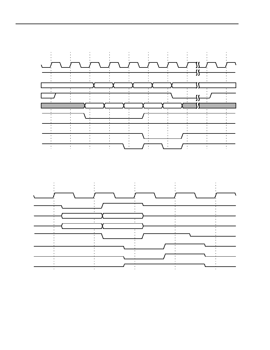
ORCA OR3TP12 FPSC
Data Sheet
Embedded Master/Target PCI Interface
March 2000
40
Lucent Technologies Inc.
Lucent Technologies Inc.
PCI Bus Core Master Controller Detailed Description
(continued)
5-7358(F)
Figure 4. Master Write Single (FIFO Interface, Quad-Port)
5-7366(F)
Figure 5. Master Write Single (PCI Bus, 32-Bit)
T0
T1
T2
T3
T4
T5
T6
T7
TN
0
1
2
6
7
0
CMD
ADRS0
ADRS1
D0
fclk
m_ready
nstatecntr
ma_fulln
mwdata
maenn
mw_fulln
mwdataenn
mwlastcycn
D1
T0
T1
T2
T3
T4
ADRS
DATA
CMD
BYTE ENABLES
clk
framen
ad
c_ben
irdyn
devseln
trdyn
stopn

Lucent Technologies Inc.
41
Data Sheet
ORCA OR3TP12 FPSC
March 2000
Embedded Master/Target PCI Interface
Lucent Technologies Inc.
PCI Bus Core Master Controller Detailed Description
(continued)
Example: Master Write, Burst Transaction
Figure 6 and Figure 7 show the timing of a Master write of four 32-bit data words, on the dual-port FPGA interface
and quad-port FPGA interface, respectively. In Figure 6, the command/address phase is initiated by the FPGA
application asserting Master address enable (maenn), while providing the Master command word on bus datafmf-
pga. On the next clock, the FPGA application provides the 32-bit address and ends the command/address phase
by asserting mwlastcycn.
To enter the data phase, maenn is deasserted, mwdataenn is asserted, and a valid 32-bit Dword of data provided
on bus datafmfpga. After the second write data word is provided, ma_fulln goes active indicating the Master will
be begin negotiating for the PCI bus (assuming mwpcihold is deaserted). The FPGA application continues to sup-
ply data (three 32-bit Dwords) on bus datafmfpga with mwdataenn asserted, while monitoring the mw_fulln flag.
To indicate the completion of the data phase, mwlastcycn is asserted, along with mwdataenn, during the final
data word.
For quad-port mode (Figure 7), the command/address and write data is transferred on the bus mwdata. The 18-bit
Master command will remain unchanged, but the 32-bit address will be split into two 16-bit components with the
LSB being transferred first. The command/address phase will require three clock cycles (with maenn asserted),
and mwlastcycn will be asserted on the final or MSB component of the address.
The quad-port data phase will also require additional clock cycles to transfer the four 32-bit write data word across
the bus mwdata. Similar to above, the data phase will be entered with the deassertion of maenn and assertion of
mwdataenn. mwlastcycn will be deasserted for all write data words, except being asserted for the final 16-bit
MSB component.
Execution begins on the PCI bus, as shown in Figure 8, which shows the timing with an external Target. The trans-
action runs to normal completion. It is a typical PCI transaction (the remote Target supports fast decode), and the
protocol and timing are as required by the PCI Specification.
5-7351(F)
Figure 6. Master Write Burst (FIFO Interface, Dual-Port)
T0
T1
T2
T3
T4
T5
T6
T7
T8
0
1
A
B
A
B
0
CMD
ADRS
D0
D1
D2
D3
fclk
m_ready
mstatecntr
ma_fulln
datafmfpga
maenn
mw_fulln
mwdataenn
mwlastcycn

ORCA OR3TP12 FPSC
Data Sheet
Embedded Master/Target PCI Interface
March 2000
42
Lucent Technologies Inc.
Lucent Technologies Inc.
PCI Bus Core Master Controller Detailed Description
(continued)
5-7359(F)
Figure 7. Master Write Burst (FIFO Interface, Quad-Port)
5-7367(F)
Figure 8. Master Write Burst (PCI Bus, 32-Bit)
T0
T1
T2
T3
T4
T5
T6
T7
T8
T9
T10
T11
T12
T13
0 1
2
6
7
8 9 6 7 8
0
D0
D2
D3
D4
D5
D6
D7
fclk
m_ready
mstatecntr
ma_fulln
mwdata
maenn
mw_fulln
mwdataenn
mwlastcycn
D1
CMD
ADRS0
ADRS1
9
T0
T1
T2
T3
T4
T5
T6
ADRS
D0
D1
D2
D3
CMD
BE0
BE1
BE2
BE3
clk
framen
ad
c_ben
irdyn
devseln
trdyn
stopn

Lucent Technologies Inc.
43
Data Sheet
ORCA OR3TP12 FPSC
March 2000
Embedded Master/Target PCI Interface
Lucent Technologies Inc.
PCI Bus Core Master Controller Detailed Description
(continued)
Table 13. Dual-Port Master Writes
1. When maenn and ma_fulln are deasserted high, the Master interface is idle.
2. When maenn is asserted low, a command/address phase is in progress.
3. maenn must be asserted low for command/address data to transfer and state to change.
4. maenn must be deasserted high and mwdataenn must be asserted low to execute the data phase and state to change.
5. Next state = 0 if mwlastcycn is asserted low (end of Master write data phase).
6. Next state = A if mwlastcycn is asserted low (end of Master command/address phase).
Table 14. Quad-Port Master Writes
1. When maenn and ma_fulln are deasserted high, the Master interface is idle.
2. When maenn is asserted low, a command/address phase is in progress.
3. maenn must be asserted low for command/address data to transfer and state to change.
4. maenn must be deasserted high and mwdataenn must be asserted low to execute the data phase and state to change.
5. Next state = 0 if mwlastcycn is asserted low (end of Master write data phase).
6. Next state = 6 if mwlastcycn is asserted low (end of Master command/address phase).
MStateCntr
Next State of
MStateCntr
Description
Data on Bus
datafmfpgax[3:0],
datafmfpga[31:0]
Notes
0
0
Idle
XXXX
4
, XXXX
16
1
0
1 or A
Command Word
Command Word [17:16], XX
2
,
Command Word [15:0], XXXX
16
2, 3, 6
1
2 or A
Address[31:0]
XXXX
4
, PCIAddress[31:0]
2, 3, 6
2
A
Address[63:32]
XXXX
4
, PCIAddress[63:32]
2, 3, 6
A
B or 0
Data[31:0]
BEN[3:0], PCIData[31:0]
4, 5
B
A or 0
Data[63:32]
BEN[7:4], PCIData[63:32]
4, 5
MStateCntr
Next State of
MStateCntr
Description
Data on Bus
mwdata[17:0]
Notes
0
0
Idle
XX
2
, XXXX
16
1
0
1 or 6
Command Word
Command Word
2, 3, 6
1
2 or 6
Address[15:0]
XX
2
, PCIAddress[15:0]
2, 3, 6
2
3 or 6
Address[31:16]
XX
2
, PCIAddress[31:16]
2, 3, 6
3
4 or 6
Address[47:32]
XX
2
, PCIAddress[47:32]
2, 3, 6
4
6
Address[63:48]
XX
2
, PCIAddress[63:48]
2, 3, 6
6
7
Data[15:0]
BEN[1:0], PCIData[15:0]
4
7
8 or 0
Data[31:16]
BEN[3:2], PCIData[31:16]
4, 5
8
9
Data[47:32]
BEN[5:4], PCIData[47:32]
4
9
6 or 0
Data[63:48]
BEN[7:6], PCIData[63:48]
4, 5
Master Read Operation
Command/Address Setup
In order to initiate a PCI Master read operation, the
FPGA application must supply the Master command,
Master read burst length, and PCI start address in the
specific order prescribed in Table 15 and Table 17, for
quad- and dual-port mode respectively. The bit defini-
tions of the Master command word are shown in
Table 10. This data is transferred via bus mwdata
(quad-port mode) or datafmfpga (dual-port mode), and
cannot be accepted by the Master FIFO interface
unless ma_fulln is inactive and m_ready is active. The
Master command word, Master read burst length, and
start address must be accompanied by assertion of the
enable maenn, with the command/address phase end-
ing with the assertion of mwlastcycn. After the com-
mand/address phase completes, ma_fulln goes active
indicating the Master will be begin negotiating for the
PCI bus.

ORCA OR3TP12 FPSC
Data Sheet
Embedded Master/Target PCI Interface
March 2000
44
Lucent Technologies Inc.
Lucent Technologies Inc.
PCI Bus Core Master Controller
Detailed Description
(continued)
The Master uses the read burst count supplied during
command/address phase to determine number of
64-bit words the Master read operation should transfer
(unlike the Master write, which uses signal mwlast-
cycn). If the burst length for a Master read operation is
the same as for the previous Master operation, the
FPGA application may elect to set bit 17 of the Master
command word. In this case, no burst length is sup-
plied; and the read burst length from the previous oper-
ation is used. This saves a clock cycle during the
command/address phase when in quad-port mode, but
should remain zero for the dual-port mode.
All read transactions require an address on a 64-bit
boundary, which requires ad2 = 0. The read burst
length will indicate the number 64-bit words to retrieve
from this address. All burst read transaction may trans-
fer twice the read burst length of 32-bit words on a
32-bit PCI bus (pci_64bit = 0). On a 64-bit PCI bus
(pci_64bit = 1), the number of transfers may equal the
read burst length. All read byte enables in the Master
command word must be asserted for a burst read
transaction.
Single 32-bit transactions require a burst length of one.
For single 32-bit reads on a 32-bit PCI bus
(pci_64bit = 0), the read byte enables MRDBEN[7:0]
can modify the start address. Using MRDBEN[7:0] =
xf0 will not modify the start address, whereas MRD-
BEN[7:0] = x0f will. For example on a 32-bit data bus
(pci_64bit = 0), a read transaction with an even 64-bit
starting address and read byte enables of 0x0f will
retrieve a 32-bit word at the starting address + 0x4. For
the case of read byte enables of 0xf0, the 32-bit word
will be retrieved from the starting address.
Read Data Phase Transfer
The FPGA application begins the read data phase by
deasserting maenn and asserting mrdataenn. On
every cycle that mrdataenn is asserted and fifo_sel is
deasserted, the FPGA application will receive read
data from the Master read FIFO (sixty-four 32-bit
words; thirty-two 64-bit words) via bus mrdata (quad-
port mode) or datatofpga (dual-port mode), providing
the read data FIFOs are not empty (mr_emptyn = 1).
No byte enables are collected from the PCI bus, and
therefore mrdata[17:16] and datatofpgax[3:0] will be
unused. mrdataenn must not be asserted when the
read data FIFOs are empty (mr_emptyn is asserted).
Note that mr_emptyn can be updated on the same
clock edge as mrdataenn is sampled.
The distinction between a burst read and a single
access is provided by the read burst length count and
the Master read byte enables. When the read burst is
greater than one, or has all of its read byte enables
asserted with pci_64bit = 0, it informs the Master of a
burst read data phase for 32-bit PCI buses. During
bursts, mrlastcycn will be deasserted for every data
element received from the Master FIFO interface while
mrdataenn is asserted (fifo_sel is deasserted), except
the last element. For a single 32-bit word transfer in
dual-port mode on a 32-bit PCI bus (pci_64bit = 0),
mrlastcycn would be asserted during the entire data
phase, since the last data phase is the only data phase
of this transfer. Note that for mrlastcycn to be
asserted, mrdataenn must be asserted.
When executing a burst Master read, or with 64-bit
agents (pci_64bit = 1), the read data transferred to the
FPGA application is always aligned on 64-bit address
boundaries, which may require transfer of extra read
data for activity on 32-bit PCI buses. For read transfers
from an odd 32-bit PCI address (ad2 = 1), this will
imply receiving an extra 32-bit read data word from the
PCI bus at the beginning of the read data phase. For
transfers starting at an even PCI address (ad2 = 0)
requiring an odd number of 32-bit data words, an extra
32-bit read data word is received at the end. The extra
read data can be discarded by the FPGA application.
For single 32-bit transactions, on 32-bit buses
(pci_64bit = 0), the Master FIFO interface will perform
the proper data alignment. The FPGA application only
needs to transfer the valid 32-bit word during the data
phase.
Master Read Data FIFO Empty/Almost Empty
When the Master read data FIFO contains four or fewer
64-bit data elements, the Master FIFO interface asserts
mr_aemptyn, the almost empty indicator. This allows
some latency to exist in the FPGA's response without
risking overreading the FIFO. When all locations in the
Master read data FIFO are empty, the Master FIFO
interface asserts mr_emptyn, the FIFO empty indica-
tor. Since data can be simultaneously written to and
read from the Master read FIFO, both mr_aemptyn
and mr_emptyn can change states in either direction
multiple times in the course of a burst data transfer.

Lucent Technologies Inc.
45
Data Sheet
ORCA OR3TP12 FPSC
March 2000
Embedded Master/Target PCI Interface
Lucent Technologies Inc.
PCI Bus Core Master Controller
Detailed Description
(continued)
Master Read Byte Enables
During Master reads, read byte enables are always
supplied by the Master to the external Target, even
though on reads the data is flowing in the opposite
direction. Thus, the byte enables cannot be buffered in
the read data FIFO alongside the corresponding data.
Also, the byte enables must be presented on the bus by
the Master at the same time that the data is being pre-
sented on the bus by the external Target (unless the
external Target uses trdyn to insert wait-states). The
data provided by the external Target cannot depend on
the byte enables unless wait-states are inserted. Since
the byte enables are not buffered, they are defined in
the Master command word (bits [11:4]) and are held
static throughout the read transaction. Their polarity is
active-low assertion.
For burst read transactions, the read byte enables must
all be asserted. Burst read transactions on a 32-bit
agent (pci_64bit = 0) are defined with a burst length of
one or greater, and the read byte enables MRD-
BEN[7:0] asserted. Mixed read byte enables are not
allowed for bursting, but are allowed for single
accesses. Single accesses for a 32-bit PCI bus
(pci_64bit = 0) are defined with a read burst length of
one, and the either of the following combination of read
byte enables: MRDBEN[7:4] = 0xf or MRDBEN[3:0] =
0xf. For 64-bit single access (pci_64bit = 1, read burst
length = 1), any combination of the read byte enables is
valid.
Wait-States
The Master will only insert wait-states into a read trans-
action when the Master read data FIFO is full, the burst
length count has not been reached, and Target is not
disconnecting. If the FPGA application cannot receive
data from the Master read data FIFOs within an eight
pciclk period, it is recommended to end the read trans-
action by asserting mr_stopburstn and mrdataen,
while storing the valid read data word, to avoid exces-
sive wait-state insertion.
Read Transaction Termination
Once initiated, Master read operations will repeat on
the PCI bus until all data is received, an abort occurs
(either Master or Target), the PCI bus' reset signal
(rstn) is asserted, or mrstopburstn is asserted. On an
abort, the Master address FIFO is cleared, but the
Master read data FIFO will continue to hold all data
received before the abort. The Master read data FIFO
must be emptied before starting a new Master transac-
tion.
mrstopburstn can be used by the FPGA application to
terminate a Master read transaction before the read
burst length has been reached. This signal is only
effective if the Master can receive data from an external
Target (irdynn and framen asserted). Since the FPGA
application has no visibility of the PCI bus control sig-
nals, mrstopburstn should be held active until
ma_fulln is deasserted.
On the Master FIFO interface, mrlastcycn indicates
when the last item of the read transaction is being
transferred, although the transaction may have ended
earlier. The transaction on the PCI bus that has been
terminated by Master is indicated by ma_fulln being
deasserted.
If a PCI transaction is terminated with a retry or discon-
nect before all data has been received, the PCI bus
core will initiate another Master read operation, con-
tinuing from that point.
Master Read FIFO Interface Reset
The FPGA application can apply a reset signal to place
the Master FIFO interface in a known state, which
clears all FIFOs and resets the mstatecntr. The reset
signal, mfifoclrn, is asynchronous and therefore
should be asserted for a minimum of one clock cycle
and deasserted for a minimum of one clock cycle
before continuing. It is not recommended to assert
mfifoclrn while a current PCI transaction is in progress
(ma_fulln asserted), since proper PCI bus termination
is not guaranteed. Only rstn will reset the internal Mas-
ter PCI state machines, while a PCI transaction is in
progress.
Example: Master Read, Single-Word Transaction
Figure 9 and Figure 10 show the timing of a Master
read, single 32-bit data word, on the dual-port FPGA
interface and quad-port FPGA interface, respectively.
In Figure 9, the command/address phase is initiated by
the FPGA application asserting Master address enable
(maenn), while providing the Master command word
and read burst length on bus datafmfpga. Assuming
the Master will decode the supplied burst length of one,
32-bit PCI bus width (pci_64bit = 0), and read byte
enable (MRDBEN[7:0] = 0xf0), this is a single opera-
tion. On the next clock, the FPGA application provides
the 32-bit address and ends the command/address
phase by asserting mwlastcycn. ma_fulln then will be
asserted, and the Master will begin negotiating for the
PCI bus.
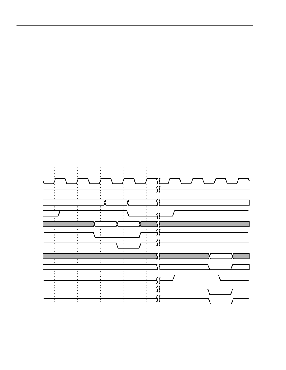
46
46
Lucent Technologies Inc.
ORCA OR3TP12 FPSC
Data Sheet
Embedded Master/Target PCI Interface
March 2000
Lucent Technologies Inc.
PCI Bus Core Master Controller
Detailed Description
(continued)
To enter the dual-port data phase, maenn is deas-
serted, mrdataenn is asserted, fifo_sel is deasserted,
and a valid 32-bit word of data will be provided on bus
datatofpga, providing the read data FIFO is not empty
(mr_emptyn = 1). For a 32-bit transfer on a
32-bit PCI bus (pci_64bit = 0), the Master FIFO inter-
face will assert the signal mrlastcycn during the only
clock of the data phase. The completion of the data
phase is indicated by mrlastcycn being asserted,
requiring mrdataenn asserted, and the final data word.
For quad-port mode (Figure 10), the command/address
phase starts with the command and read burst length
transferring on the bus mwdata in sequential 18-bit
segments. The 18-bit Master command will be trans-
ferred first on mwdata, followed the 18-bit read burst
length, with both validated by an asserted maenn. The
32-bit address will be split into two 16-bit components
with the LSB being transferred first, also validated by
an asserted maenn. The command/address phase will
require four clock cycles, and mwlastcycn will be
asserted on the final or MSB component of the
address.
In the data phase of the quad-port mode, the read data
will be transferred in 16-bit segments on bus mrdata.
The read data phase will require two clock cycles to
transfer the 32-bit read data word across the 16-bit bus
mrdata, providing mrdataen is asserted, and the read
data FIFOs are not empty (mr_emptyn = 1). mrlast-
cycn will be deasserted for the first 16-bit LSB of the
read data word, and asserted for the final 16-bit MSB
component.
Following this command/address setup, execution
begins on the PCI bus. Figure 11 shows the timing of a
typical transaction with a remote Target. The transac-
tion results in a normal completion. The remote Target
supports fast decode, and the protocol and timing are
as required by the PCI Specification.
5-7352(F)
Figure 9. Master Read Single (FIFO Interface, Dual-Port)
T0
T1
T2
T3
T4
TN
TN+1
TN+2
TN+3
0
1
0
0
BRST/CMD
ADRS
DATA
fclk
m_ready
mstatecntr
ma_fulln
datafmfpga
maenn
mwlastcycn
datatofpga
fifo_sel
mr_emptyn
mrdataenn
mrlastcycn

Lucent Technologies Inc.
47
Data Sheet
ORCA OR3TP12 FPSC
March 2000
Embedded Master/Target PCI Interface
Lucent Technologies Inc.
PCI Bus Core Master Controller Detailed Description
(continued)
5-7360(F)
Figure 10. Master Read Single (FIFO Interface, Quad-Port)
5-7368(F)
Figure 11. Master Read Single (PCI Bus, 32-Bit)
T0
T1
T2
T3
T4
T5
TN+0
TN+0
TN+1
TN+2
TN+3
TN+4
0
1
2
3
0
1
0
CMD
BRST
ADRS0 ADRS1
D0
D1
fclk
m_ready
mstatecntr
ma_fulln
mwdata
maenn
mwlastcycn
mrdata
mr_emptyn
mrdatenn
mrlastcycn
T0
T1
T2
T3
T4
T5
ADRS
DATA
CMD
BYTE ENABLES
clk
framen
ad
c_ben
irdyn
devseln
trdyn
stopn

48
48
Lucent Technologies Inc.
ORCA OR3TP12 FPSC
Data Sheet
Embedded Master/Target PCI Interface
March 2000
Lucent Technologies Inc.
PCI Bus Core Master Controller
Detailed Description
(continued)
Example: Master Read, Burst Transaction
Figure 12 and Figure 13 show the timing of a four 32-bit
word Master burst read, on the dual-port FPGA inter-
face and quad-port FPGA interface, respectively. Oper-
ation is similar to that in the Master read, single-word
transaction, but extra data Dwords are requested by
the FPGA application. In Figure 12, the command/
address phase is initiated by the FPGA application
asserting Master address enable (maenn), while pro-
viding the Master command word and read burst length
on bus datafmfpga. Assuming, the Master will decode
a supplied burst length of two, and read byte enable
(MRDBEN[7:0] = 0x00), this is a burst operation. On
the next clock, the FPGA application provides the
32-bit address and ends the command/address phase
by asserting mwlastcycn. ma_fulln then will be
asserted, and the Master will begin negotiating for the
PCI bus.
To enter the dual-port read data phase, maenn is
deasserted, mrdataenn is asserted, and valid 32-bit
data words will be provided on bus datatofpga
(fifo_sel = 0), providing the read data FIFO is not
empty (mr_emptyn = 1). For a burst transfer, the Mas-
ter FIFO interface will assert the signal mrlastcycn
during the last clock of the data phase, and deasserted
otherwise. The completion of the data phase is indi-
cated by mrlastcycn asserted, requiring mrdataenn
asserted, and the final data word.
For quad-port mode (Figure 13), the command/address
phase starts with the command and read burst length
transferring on the bus mwdata in sequential seg-
ments. The 18-bit Master command will be transferred
first on mwdata, followed the 18-bit read burst length,
with both validated by an asserted maenn. The 32-bit
address will be split into two 16-bit components with
the LSB being transferred first, also validated by an
asserted maenn. The command/address phase will
require four clock cycles, and mwlastcycn will be
asserted on the final or MSB component of the
address.
In the read data phase of the quad-port mode, the read
data will be transferred in 16-bit segments on bus
mrdata. The read data phase will require two clock
cycles to transfer each 32-bit read data word across the
16-bit bus mrdata, providing mrdataen is asserted, the
read data FIFOs are not empty (mr_emptyn = 1).
mrlastcycn will be deasserted for the all cycles of the
data phase, and asserted for final the 16-bit MSB com-
ponent.
Following this command/address setup, execution
begins on the PCI bus. Figure 14 shows the timing of a
typical transaction with a remote Target. The transac-
tion results in a normal completion. The remote Target
supports fast decode, and the protocol and timing are
as required by the PCI Specification.

Lucent Technologies Inc.
49
Data Sheet
ORCA OR3TP12 FPSC
March 2000
Embedded Master/Target PCI Interface
Lucent Technologies Inc.
PCI Bus Core Master Controller Detailed Description
(continued)
5-7353(F)
Figure 12. Master Read Burst (FIFO Interface, Dual-Port)
T0
T1
T2
T3
T4
TN
TN+1
TN+2
TN+3
TN+4
TN+5
0
1
0
0
1
0
1
0
BRST/CMD
ADRS
D0
D1
D2
D3
fclk
m_ready
mstatecntr
ma_fulln
datafmfpga
maenn
mwlastcycn
datatofpga
fifo_sel
mr_emptyn
mrdataenn
mrlastcycn

ORCA OR3TP12 FPSC
Data Sheet
Embedded Master/Target PCI Interface
March 2000
50
Lucent Technologies Inc.
Lucent Technologies Inc.
PCI Bus Core Master Controller Detailed Description
(continued)
5-7361(F)
Figure 13. Master Read Burst (FIFO Interface, Quad-Port)
T0
T1
T2
T3
T4
T5
T6
T7
T8
T9
T10
T11
T12
T13
T14
T15
T16
0
1
2
3
0
1
2
3
0
1
2
3
0
ADRS0 ADRS1
D0
D1
D2
D3
D4
D5
D6
D7
fclk
m_ready
mstatecntr
ma_fulln
mwdata
maenn
mwlastcycn
mrdata
mr_emptyn
mrdataenn
mrlastcycn
CMD
BRST

Lucent Technologies Inc.
51
Data Sheet
ORCA OR3TP12 FPSC
March 2000
Embedded Master/Target PCI Interface
Lucent Technologies Inc.
PCI Bus Core Master Controller Detailed Description
(continued)
5-7369(F)
Figure 14. Master Read Burst (PCI Bus, 32-Bit)
Table 15. Dual-Port Master Read, Specified Burst Length
1. When maenn, mrdataenn, and ma_fulln are deasserted high, the Master interface is idle.
2. When maenn is asserted low, a command/address phase is in progress.
3. maenn must be asserted low for command/address data to transfer and state to change.
4. maenn must be deasserted high and mrdataenn must be asserted low to execute the data phase.
5. Next state = 0 if mrlastcycn is asserted low (end of Master read data phase).
6. Next state = 0 if mwlastcycn is asserted low (end of Master command/address phase).
MStateCntr
Next State of
MStateCntr
Description
Data on Bus
datafmfpgax[3:0]
datafmfpga[31:0]
Data on Bus
datatofpga[31:0]
Notes
0
0
Idle,
or Data[15:0]
X
4
XXXXXXXX
16
PCIData[31:0]
1, 4, 5
0
1 or 0
Burst Length,
Command Word,
or Data[63:32]
Burst Length,
Command Word
PCIData[63:32]
2, 3, 4, 5,
6
1
0 or 2
Address[31:0]
X
4
, PCIAddress[31:0]
--
2, 3, 6
2
0
Address[63:32]
X
4
, PCIAddress[63:32]
--
2, 3, 6
T0
T1
T2
T3
T4
T5
T6
T7
T8
ADRS
D0
D1
D2
D3
CMD
BE0
BE1
BE2
BE3
clk
framen
ad
c_ben
irdyn
devseln
trdyn
stopn

ORCA OR3TP12 FPSC
Data Sheet
Embedded Master/Target PCI Interface
March 2000
52
Lucent Technologies Inc.
Lucent Technologies Inc.
PCI Bus Core Master Controller Detailed Description
(continued)
Table 16. Quad-Port Master Read, Duplicate Burst Length
1. When maenn, mrdataenn, and ma_fulln are deasserted high, the Master interface is idle.
2. When maenn is asserted low, a command/address phase is in progress.
3. maenn must be asserted low for command/address data to transfer and state to change.
4. maenn must be deasserted high and mrdataenn must be asserted low to execute the read data phase.
5. Next state = 0 if mrlastcycn is asserted low (end of Master read data phase).
6. Next state = 0 if mwlastcycn is asserted low (end of Master command/address phase).
Table 17. Quad-Port Master Read, Specified Burst Length
1. When maenn, mrdataenn, and ma_fulln are deasserted high, the Master interface is idle.
2. When maenn is asserted low, a command/address phase is in progress.
3. maenn must be asserted low for command/address data to transfer and state to change.
4. maenn must be deasserted high and mrdataenn must be asserted low to execute the read data phase.
5. Next state = 0 if mrlastcycn is asserted low (end of Master read data phase).
6. Next state = 0 if mwlastcycn is asserted low (end of Master command/address phase).
MStateCntr
Next State of
MStateCntr
Description
Data on Bus
mwdata[17:0]
Data on Bus
mrdata[15:0]
Notes
0
0
Idle
XX
2
XXXX
16
--
1
0
1 or 0
Command Word
or Data[15:0]
Command Word
PCIData[15:0]
2, 3, 4, 5, 6
1
2 or 0
Address[15:0] or
Data[31:16]
XX
2
, PCIAddress[15:0]
PCIData[15:0]
2, 3, 4, 5, 6
2
3 or 0
Address[31:16] or
Data[47:32]
XX
2
, PCIAddress[15:0]
PCIData[47:32]
2, 3, 4, 5, 6
3
4 or 0
Address[47:32] or
Data[63:48]
XX
2
, PCIAddress[47:32]
PCIData[63:48]
2, 3, 4, 5, 6
4
0
Address[63:48]
XX
2
, PCIAddress[63:48]
--
2, 3, 6
MStateCntr
Next State of
MStateCntr
Description
Data on Bus
mwdata[17:0]
Data on Bus
mrdata[15:0]
Notes
0
0
Idle
XX
2
XXXX
16
--
1
0
1
Command Word
or Data[15:0]
Command Word
PCIData[15:0]
2, 3, 4, 5, 6
1
2 or 0
Burst Length or
Data[31:16]
Burst Length
PCIData[31:16]
2, 3, 4, 5, 6
2
3 or 0
Address[15:0] or
Data[47:32]
XX
2
, PCIAddress[15:0]
PCIData[47:32]
2, 3, 4, 5, 6
3
4 or 0
Address[31:16] or
Data[63:48]
XX
2
, PCIAddress[15:0]
PCIData[63:48]
2, 3, 4, 5, 6
4
5 or 0
Address[47:32] or
Data[63:48]
XX
2
, PCIAd-
dress[47:32]
--
2, 3, 6
5
0
Address[63:48]
XX
2
, PCIAd-
dress[63:48]
--
2, 3, 6

Lucent Technologies Inc.
53
Data Sheet
ORCA OR3TP12 FPSC
March 2000
Embedded Master/Target PCI Interface
Lucent Technologies Inc.
PCI Bus Core Target Controller Detailed
Description
Target FIFO Interface
Overview
The Target FIFO interface consists of two transfer
phases: command/address followed by data. This
sequence must be followed with the assertion of
twlastcycn indicating the completion of each phase.
The PCI address and command are always provided by
the Target FIFO interface with the address transferred
on the data paths for the specific mode. In any port
mode, the command and address are transferred dur-
ing the same cycle with the Target command trans-
ferred on a separate bus tcmd. The command/address
phase is followed by data transfer. For Target writes,
write data with byte enables will be provided from the
Target, whereas for Target reads, the Target will receive
its data from the FPGA application. All types of data
are transferred on the data paths defined by the opera-
tional mode (dual- or quad-port).
Target State Counter
The Target FIFO interface provides a state counter,
tstatecntr[3:0], that informs the FPGA application of
its current state (Table 19). This state counter deter-
mines what data is being provided to the FPGA appli-
cation by the Target FIFO interface during the
command/address or write data phases, or what is
expected from the FPGA application during the read
data phases. The state counter transitions from one
state to another in a predetermined manner. Table 20
through Table 23 detail the sequencing of the tstate-
cntr and the data transferred for Target write and read
transactions.
The value on bus tstatecntr can be used to minimize
FPGA logic or verify proper operation. The data pro-
vided by the Target FIFO interface to the FPGA appli-
cation is accompanied by a value on tstatecntr[3:0].
This value can be directly used by the FPGA applica-
tion to determine the proper orientation of the Target
command, address and/or write data. This eliminates
the need for logic in the FPGA to duplicate a state
counter. The data required from the FPGA application
by the Target during the read data phase is also
defined by the value on tstatecntr. However, the state
counter value being sent to the FPGA is in the same
cycle that the data is sent from the FPGA application.
Here, the value provided by the Target FIFO interface
can be used to determine the next state, since current
since current data, phase, enables, and state transi-
tions are known.
Target Address Compare and BAR Size
The Target FIFO interface provides the following two
features to reduce overhead when transferring the PCI
start Target address during the command/address
phase. First, the Target FIFO interface detects the page
size of the base address register (BAR) that decoded
the current PCI address, and only transfers the address
bytes necessary to cover the page size.
Second, the Target FIFO interface provides a holding
register which is used to compare the address of the
previous Target transaction to the current one. If there
is a match, the most signification address information is
not transferred, providing the BAR size is greater than
the data bus size for quad- or dual-port mode. This will
cover address bits [63:48] in quad-port and bits [63:32]
in the dual-port mode. This option is enabled through
the FPSC configuration manager of the FPSC design
kit.
Target Write Operation
Delayed Transactions, Target Memory Write
Target memory write operations cannot be processed
as delayed (delayed transactions: PCI Specification
2.2: Section 3.3.3.3), and are always posted. The Tar-
get will only retry a memory write transaction if a cur-
rent Target transaction is in progress (treqn is
asserted) or t_retryn is asserted. Once the Target
determines that it is the intended recipient, it asserts
devseln and trdyn and begins storing data into the
Target write FIFO, providing space is available.
Delayed Transactions, Target I/O Write
Target I/O write operations can be posted (deltrn = 1)
or delayed (deltrn = 0), and always disconnect burst
accesses into single accesses. For a delayed I/O write,
the Target records the PCI bus command, address, and
first data word (32 or 64 bits) along with its byte
enables (4 or 8 bits) during the initial access. The PCI
bus command and address are put in the Target
address FIFO, and the data word and byte enables are
put in the Target write FIFO. On the PCI bus, the
request is terminated in a retry (with the Master
unaware that the data was snooped), and the FPGA
application is informed that a Target request is pending
via the assertion of treqn. The transaction status at this
time is DWR (delayed write request--see PCI Specifi-
cation 2.2: Section 3.3.3.3.6), and subsequent
requests will be terminated in retry until the FPGA
application processes the Target transaction.

54
54
Lucent Technologies Inc.
ORCA OR3TP12 FPSC
Data Sheet
Embedded Master/Target PCI Interface
March 2000
Lucent Technologies Inc.
PCI Bus Core Target Controller Detailed
Description
(continued)
When the FPGA application reads the Target write
FIFO and empties it, the transaction status changes to
DWC (delayed write completion), and the next Target
I/O write that matches the stored command, address,
data, and byte enables will be disconnected with data,
completing the transaction and clearing the Target
address and Target write FIFOs.
Target Configuration Writes
Accesses of configuration space occur without any
involvement of the FPGA application. All configuration
space accesses are disconnected with data on the first
data word and are thus restricted from bursting.
Target Write Wait-States
All Target write data is accepted with zero wait-states.
When a Target memory write operation fills the Target
write FIFO, future response depends on signal
twburstpendn. If it is deasserted, the Target will gen-
erate a disconnect without data on the next data cycle.
If it is asserted, the Target will insert up to eight wait-
states and then disconnect without data if the FIFO
remains full. Target I/O operations cannot fill the FIFO
because they do not burst, disconnecting with data on
the first Dword.
Command/Address Setup
When the Target has accepted a PCI Target transac-
tion, it will inform the FPGA application by asserting the
signal treqn. The FPGA application can then transfer
the PCI start address, Target command word, and data
in the specific order prescribed in Table 20 through
Table 23, for the operational mode (quad- and dual-
port). The address data is transferred via bus twdata
(quad-port mode) or datatofpga (dual-port mode with
fifo_sel = 1) when taenn is asserted. taenn should
only be asserted when treqn is active and t_ready is
active. The command/address phase ends with the
assertion of twlastcycn. The Target command word
(PCI bus command) and decoded BAR register are
transferred on the separate buses, tcmd and bar
respectively, and are valid when treqn is active.
The number of cycles necessary to send the Target
address can vary. The Target FIFO interface will ana-
lyze the size of the decoded BAR and perform the min-
imal number of cycles to completely transfer the page
of the address. For example, if the BAR is 256K in size,
only the lower 18 bits of address is required by the
FPGA application. This will result in one clock address
transfer for dual-port (32-bits) and two for the quad-port
(16-bits).
Accompanying the address data during the assertion of
taenn, is information on the current Target transaction
(Table 18). Dual-address or 64-bit address is indicated
during the address phase by twdata[16] (quad-port) or
datatofpgax[0] (dual-port with fifo_sel = 1) being
asserted. If the current transaction is a burst,
twdata[17] (quad-port) or datatofpgax[1](dual-port
with fifo_sel = 1) will be asserted.
All burst transactions (burst indication bit active) and
64-bit agents (pci_64bit = 1) will have the Target data
aligned on a 64-bit address boundary (ad2 = 0), even if
the PCI start address starts on a 32-bit address with
ad2 = 1. If the burst transaction on the PCI bus starts
on a odd 32-bit address boundary (ad2 = 1), the data
phase start address will be on a 64-bit address bound-
ary (ad2 = 0). Likewise, the data phase will also end on
a 64-bit address boundary, therefore the number of
transfers between the Target FIFO interface and the
FPGA application will always be even for burst transac-
tions and 64-bit agents (PCI_64bit = 1).
Table 18. Bit Destinations for Target Command/Address Phase
* Refer to PCI Specification 2.2 Section 3.1.
Bits
Name
Description
Quad-Port
Dual-Port
Target Address Word (PCI Core
FPGA)
17
BI
Burst Indication
twdata[17]
datatofpgax[1]
16
DA
Dual-Address Indication
twdata[16]
datatofpgax[0]
15:0
Adrs
Address
twdata[15:0]
datatofpga[31:0]
Target Command Word (PCI Core
FPGA)
3:0
Cmd
PCI Command Code*
tcmd[3:0]
tcmd[3:0]

Lucent Technologies Inc.
55
Data Sheet
ORCA OR3TP12 FPSC
March 2000
Embedded Master/Target PCI Interface
Lucent Technologies Inc.
PCI Bus Core Target Controller Detailed Description
(continued)
For a write burst transaction to an odd address (ad2 = 1), the first write data word transferred to the FPGA applica-
tion will have all its byte enables deasserted and can be discarded. For Target read transactions to an odd address
(ad2 = 1), the first read data word provided by the FPGA application is discarded by the Target FIFO interface.
For single transaction (burst indication bit deasserted) on 32-bit PCI bus (pci_64bit = 0), the Target FIFO interface
handles all data alignment. The received address is valid as transferred, with the data phase aligning to this
address. No extra data is transferred or discarded.
Table 19. Target State Counter (TStateCntr) Values and the Corresponding Bus Data
TStateCntr[3:0]
Dual-Port Mode (32-bit Ports)
Quad-Port Mode (16-bit Ports)
Data on Bus
datatofpga
Data on Bus
datafmfpga
Data on Bus
twdata
Data on Bus
trdata
0
Adrs[31:0]
Data[31:0]
Adrs[15:0]
Data[15:0]
1
Adrs[63:32]
Data[63:32]
Adrs[31:16]
Data[31:16]
2
--
--
Adrs[47:32]
Data[47:32]
3
--
--
Adrs[63:48]
Data[63:48]
4
Data[31:0]
--
Data[15:0]
--
5
Data[63:32]
--
Data[31:16]
--
6
--
--
Data[47:32]
--
7
--
--
Data[63:48]
--
8
--
--
--
--
9
--
--
--
--
A
--
--
--
--
B
--
--
--
--
C
--
--
--
--
D
--
--
--
--
E
--
--
--
--
F
--
--
--
--

ORCA OR3TP12 FPSC
Data Sheet
Embedded Master/Target PCI Interface
March 2000
56
Lucent Technologies Inc.
Lucent Technologies Inc.
PCI Bus Core Target Controller Detailed
Description
(continued)
Write Data Transfer
The FPGA application enters the write data phase by
deasserting taenn and asserting twdataenn. On every
cycle that twdataenn is asserted, the FPGA applica-
tion receives write data and its associated byte enables
from the Target write data FIFO (64 32-bit words; 32
64-bit words) via bus twdata (quad-port mode) or
datatofpga (dual-port mode with fifo_sel = 1), provid-
ing the write data FIFOs are not empty (tw_emptyn =
1). twdataenn must not be asserted when the write
data FIFOs are empty (tw_emptyn is asserted). Note
that tw_emptyn can be updated on the same clock
edge as twdataenn is sampled.
The distinction between a burst write and a single
access is provided by the burst indication bit
(twdata[17] (quad-port); datatofpgax[1] (dual-port
with fifo_sel = 1), or behavior of the twlastcycn signal
during the data phase. When twlastcycn is asserted,
this signal informs the FPGA application of the end of
the write data phase. twlastcycn will remain deas-
serted with every write data element except the last
element on bus twdata (quad-port mode) or datatof-
pga (dual-port mode with fifo_sel = 1). For example,
on a single 32-bit word transfer in dual-port mode,
twlastcycn would be asserted during the entire write
data phase, since the last data phase is the only data
phase of this transfer.
When executing on a 64-bit PCI bus (pci_64bit = 1) or
a burst Target write, the write data transferred from the
FPGA application is aligned on 64-bit address bound-
aries. This alignment may transfer extra padding data
from the FIFOs for activity during 32-bit PCI transfers.
For transfers starting at an odd 32-bit PCI address
(ad2 = 1), the FPGA application will receive a 32-bit
padding data word at the beginning of the write data
phase. For burst transfers starting at an even PCI
address (ad2 = 0) with an odd number of 32-bit data
words, a 32-bit padding data word will be received at
the end of the data phase. Padding data words are indi-
cated by data words with all of its byte enables deas-
serted.
For single 32-bit transactions (Burst indication bit deas-
serted) on 32-bit PCI buses (pci_64bit = 0), the Target
FIFO interface will perform proper data alignment. Dur-
ing the data phase, the FPGA application will only
receive the 32-bit data word, and no padding words are
present.
Target Write Data FIFO Empty/Almost Empty
When the Target write FIFO contains four or fewer
64-bit data elements, the Target FIFO interface asserts
tw_aemptyn the FIFO almost empty indicator. This
allows some latency to exist in the FPGA's response
without risking overreading the FIFO. When the FPGA
application has read all data out of the Target write
FIFO, the Target FIFO interface asserts tw_emptyn,
the FIFO empty indicator. Since data can be simulta-
neously written to, and read from, the Target write
FIFO, both tw_aemptyn and tw_emptyn can change
states in either direction multiple times in the course of
a burst data transfer.
Target Write Termination
Target write termination will be by normal Master termi-
nation, disconnect associated with a full Target write
data FIFO, retry associated with a pending Target
transaction, or a reset by rstn.
On the Target FIFO interface, twlastcycn signals when
the last item remaining in the Target write FIFO has
been received by the FPGA application (although the
actual PCI bus transaction may have completed much
earlier). The Target FIFO interface then signals end of
transaction to the FPGA application by deasserting
treqn for at least one clock. If treqn subsequently reas-
serts, this indicates a new, unrelated transaction.
Reset
The FPGA application can apply a reset signal to place
the Target FIFO interface logic in a known state, clear-
ing the Target FIFOs and resetting tstatecntr. The
reset signal, tfifoclrn, is asynchronous and therefore
should be asserted for a minimum of one clock cycle
and deasserted for a minimum of one clock cycle
before continuing.
It is not recommended to assert tfifoclrn while a cur-
rent PCI transaction is in progress (treqn is asserted),
since proper PCI bus termination is not guaranteed.
Only rstn will reset the internal Target PCI state
machines, while a PCI transaction is in progress.

Lucent Technologies Inc.
57
Data Sheet
ORCA OR3TP12 FPSC
March 2000
Embedded Master/Target PCI Interface
Lucent Technologies Inc.
PCI Bus Core Target Controller Detailed Description
(continued)
Example: Target Write to Configuration Space Transaction
Figure 15 shows the timing on the PCI interface for a Target write to configuration space. Configuration space
accesses occur without any involvement of the FPGA interface. All configuration space accesses are disconnected
with data on the first data word and are thus restricted from bursting. Address decode speed is medium, and the
Target signals that it is ready to receive the word of data by asserting trdyn one cycle after devseln is asserted.
5-7370(F)
Figure 15. Target Configuration Write (PCI Bus, 32-Bit)
T0
T1
T2
T3
T4
T5
T6
ADDRESS
DATA
CFG WR
BYTE ENABLES
clk
framen
ad
c_ben
idsel
irdyn
devseln
trdyn
stopn

ORCA OR3TP12 FPSC
Data Sheet
Embedded Master/Target PCI Interface
March 2000
58
Lucent Technologies Inc.
Lucent Technologies Inc.
PCI Bus Core Target Controller Detailed Description
(continued)
Example: Target Write I/O
Figure 16 shows the timing on the PCI bus for a Target I/O write which is posted; that is, the operation completes on
the PCI bus immediately. The Target terminates the I/O write request by disconnecting with data on the first word,
thus disallowing bursting.
For a delayed Target I/O write, the initial access would terminate with a retry although the Target transaction has
been snooped and forwarded on to the FPGA application. Retry terminations will continue on all future accesses
until the FPGA application has finished processing the Target I/O write transaction. On the next access of this Tar-
get I/O write, the Target terminates the I/O write request by disconnecting with data on the first word, also disallow-
ing bursting.
The FPGA interface timing is as shown in Figure 18 and Figure 19 for dual- and quad-port respectively. The FPGA
interface timing is similar for Target I/O writes and Target single memory writes, and is described below in the
Single Target Write FIFO Interface section.
5-7371(F)
Figure 16. Target I/O Write, Nondelayed (PCI Bus, 32-Bit)
T0
T1
T2
T3
T4
T5
T6
ADDRESS
DATA
IO WR
BYTE ENABLES
clk
framen
ad
c_ben
irdyn
devseln
trdyn
stopn

Lucent Technologies Inc.
59
Data Sheet
ORCA OR3TP12 FPSC
March 2000
Embedded Master/Target PCI Interface
Lucent Technologies Inc.
PCI Bus Core Target Controller Detailed Description
(continued)
Target Write Memory, Single-Word Transaction
Figure 17 shows the timing on the PCI bus, for a Target memory write of a single word. The timing on the PCI inter-
face (Figure 17) is similar to that of a posted I/O write (Figure 16) except that, since bursts to memory space are
allowed, the signal stopn is not asserted.
5-7373(F)
Figure 17. Target Memory Single Write (PCI Bus, 32-Bit)
Single Target Write FIFO Interface
The FIFO interface timing is as shown in Figure 18 and Figure 19 for dual- and quad-port respectively. The inter-
face timing is similar for all Target I/O writes and Target single memory writes, since the Target FIFO interface is
uniform across all Target accesses.
The timing on the interface (Figure 18 for dual-port) shows the first indication to the FPGA application that a new
operation is pending by the assertion of Target request (treqn). When treqn is valid, the FPGA application begins
the command/address phase by asserting Target address enable (taenn) and accepting the command from bus
tcmd and address from bus datatofpga(x) (with fifo_sel = 1). If applicable, the dual-address indication bit accom-
panies the address on datatofpga[0], whereas for the single access on a 32-bit PCI bus (pci_64bit = 0) the burst
indication bit (datatofpga[1]) will be desasserted. The FPGA application continues to receive new address data
(taenn asserted) on every clock until twlastcycn is asserted, indicating the end of the command/address phase.
See command/address section for notes regarding address transfer and alignment.
The write data phase will follow, by deassertion of taenn, and assertion of Target write data enable (twdataenn).
twdataenn can only be asserted while tw_emptyn is deasserted, indicating that write data is available in the write
data FIFOs. While twdataenn is asserted, the FPGA application will receive Target write data on bus datatofpga
(with fifo_sel = 1). The FPGA application is informed that the last component of the data phase is being presented
when twlastcycn is asserted. Since this is a single access on a 32-bit data bus (assuming datatofpgax[1] = 0 dur-
ing command/address phase, pci_64bit = 0), the first and only data phase is the last data of the write data phase.
T0
T1
T2
T3
T4
T5
ADDRESS
DATA
MEM WR
BYTE ENABLES
clk
framen
ad
c_ben
irdyn
devseln
trdyn
stopn

ORCA OR3TP12 FPSC
Data Sheet
Embedded Master/Target PCI Interface
March 2000
60
Lucent Technologies Inc.
Lucent Technologies Inc.
PCI Bus Core Target Controller Detailed Description
(continued)
For quad-port mode (Figure 19), the address and write data are transferred on the bus twdata in 16-bit segments.
The address will be split into two 16-bit components with the LSB being transferred first. If applicable, the dual-
address indication accompanies the address on twdata[16], whereas for a single access on a 32-bit PCI bus
(pci_64bit = 0) the burst indication bit (twdata[17]) will be deasserted. Assuming a BAR size greater than 16 bits,
the address phase will require two clock cycles, and twlastcycn will be asserted on the final or MSB component of
the address.
The data phase will also require two clock cycles to transfer a single 32-bit write data word across the 16-bit bus.
twdataenn can only be asserted while tw_emptyn is deasserted, indicating that write data is available in the write
data FIFOs. While twdataenn is asserted, the FPGA application will receive Target write data on bus twdata.
twlastcycn will be deasserted for all 16-bit components of the write data phase, except for the final 16-bit compo-
nent, where it is asserted.
5-7354(F)
Figure 18. Target Write Single (FIFO Interface, Dual-Port)
1
T0
T1
T2
T3
0
4
0
CMD
ADRS
DATA
fclk
t_ready
tstatecntr
treqn
tcmd
datatofpga
fifo_sel
taenn
tw_emptyn
twdataenn
twlastcycn

Lucent Technologies Inc.
61
Data Sheet
ORCA OR3TP12 FPSC
March 2000
Embedded Master/Target PCI Interface
Lucent Technologies Inc.
PCI Bus Core Target Controller Detailed Description
(continued)
5-7362(F)
Figure 19. Target Write Single (FIFO Interface, Quad-Port)
Example: Target Write Memory Burst Transaction
Figure 20 shows the timing on the PCI bus for a Target memory write burst of four 32-bit words. The timing on the
PCI interface is typical for a medium-speed decode Target. Note that trdyn is asserted at the earliest possible time,
which is concurrent with assertion of devseln. In the example of a 4-word burst, the Target write FIFO is not filled,
so execution continues to completion. This would also be the case for a burst of any length when the FPGA appli-
cation is capable of unloading the FIFO as fast as the PCI interface is loading it. If the Target write FIFO becomes
full, the Target can disconnect without data on the first data word it cannot accept (twburstpendn = 1), or insert up
to eight wait-states (twburstpendn = 0).
The timing on the dual-port FIFO interface (Figure 21) shows the first indication to the FPGA application that a new
operation has begun by the assertion of Target request (treqn). When treqn is valid, the FPGA application begins
the command/address phase by asserting Target address enable (taenn) and accepting the command from bus
tcmd and address from bus datatofpga(x) (with fifo_sel = 1). A burst operation and dual-address indication
accompanies the address on datatofpgax[1] and datatofpgax[0] respectively. The FPGA application continues to
receives new address data (taenn asserted) on every clock until twlastcycn is asserted, indicating the end of the
command/address phase. See command/address section for notes regarding address transfer and alignment.
1
T0
T1
T2
T3
T4
T5
0
1
4
5
0
CMD
ADRS0
ADRS1
D0
D1
fclk
tstatecntr
t_ready
treqn
tcmd
twdata
taenn
tw_emptyn
twdataenn
twlastcycn

ORCA OR3TP12 FPSC
Data Sheet
Embedded Master/Target PCI Interface
March 2000
62
Lucent Technologies Inc.
Lucent Technologies Inc.
PCI Bus Core Target Controller Detailed Description
(continued)
The write data phase will follow, by deassertion of taenn, and assertion of Target write data enable (twdataenn).
twdataenn can only be asserted while tw_emptyn is deasserted, indicating that write data is available in the write
data FIFOs. While twdataenn is asserted, the FPGA application will receive Target write data on bus datatofpga
(with fifo_sel = 1), and write byte enables on datatofpgax. The FPGA application is informed that the last compo-
nent of the data phase is being presented when twlastcycn is asserted. Since this is a burst access (datatofp-
gax[1] = 1 during command/address phase), the twlastcycn is deasserted for the entire data phase expect the
last data of the write data phase. After receiving twlastcycn at the end of the data phase, twdataenn must be
deasserted by the FPGA application. See Write Data Transfer section for notes regarding data alignment on bursts.
For quad-port mode (Figure 22), the address and write data is transferred on the bus twdata in 16-bit segments. If
necessary, the address will be split into two 16-bit components with the LSB being transferred first. A burst opera-
tion and dual-address indication accompanies the address on twdata[17] and twdata[16] respectively. Assuming
the BAR size is greater than 16 bits, the address phase will require two clock cycles, and twlastcycn will be
asserted on the final or MSB component of the address. The data phase will also require two clock cycles to trans-
fer every 32-bit write data word across the 16-bit bus. twlastcycn will be deasserted for all 16-bit components of
the write data phase, except for the final 16-bit component where it is asserted. See Write Data Transfer section for
notes regarding write data alignment.
5-7374(F)
Figure 20. Target Memory Write Burst (PCI Bus, 32-Bit)
T0
T1
T2
T3
T4
T5
T6
T7
T8
ADDRESS
D0
D1
D2
D3
MEM WR
BE0
BE1
BE2
BE3
clk
framen
ad
c_ben
irdyn
devseln
trdyn
stopn

Lucent Technologies Inc.
63
Data Sheet
ORCA OR3TP12 FPSC
March 2000
Embedded Master/Target PCI Interface
Lucent Technologies Inc.
PCI Bus Core Target Controller Detailed Description
(continued)
5-7355(F)
Figure 21. Target Write Burst (FIFO Interface, Dual-Port)
1
T0
T1
T2
T3
T4
T5
T6
T7
0
4
5
4
5
0
CMD
ADRS
D0
D1
D2
D3
fclk
t_ready
tstatecntr
treqn
tcmd
datatofpga
fifo_sel
taenn
tw_emtpyn
twdataenn
twlastcycn

ORCA OR3TP12 FPSC
Data Sheet
Embedded Master/Target PCI Interface
March 2000
64
Lucent Technologies Inc.
Lucent Technologies Inc.
PCI Bus Core Target Controller Detailed Description
(continued)
5-7363(F)
Figure 22. Target Write Burst (FIFO Interface, Quad-Port)
Table 20. Dual-Port Target Write
1. When treqn is deasserted high, the Target interface is idle.
2. When taenn is asserted low, a command/address phase is in progress.
3. taenn must be asserted low for command/address data to transfer and state to change.
4. taenn must be deasserted high and twdataenn must be asserted low to execute the data phase.
5. Next state = 0 if twlastcycn is asserted low (end of Target write data).
6. Next state = 4 if twlastcycn is asserted low (end of Target command/address phase).
tstatecntr
Next State or
tstatecntr
Description
Data on Bus
datafmfpgax[3:0],
datafmfpga[31:0]
Notes
0
0
Idle
X
4
, XXXXXXXX
16
1
0
1 or 4
Address[31:0]
X
2
, Burst, Dual-Address,
PCIAddress[31:0]
2, 3, 6
1
4
Address[63:32]
X
2
, Burst, Dual-Address,
PCIAddress[63:32]
2, 3, 6
4
5 or 0
Data[31:0]
BEN[3:0], PCIData[31:0]
4, 5
5
4 or 0
Data[63:32]
BEN[7:4], PCIData[63:32]
4, 5
1
T0
T1
T2
T3
T4
T5
T6
T7
T8
T9
T10
0
1
4
5
6
7
4
5
6
7
0
CMD
ADRS0
ADRS1
D0
D1
D2
D3
D4
D5
D6
D7
fclk
t_ready
tstatecntr
treqn
tcmd
twdata
taenn
tw_emptyn
twdataenn
twlastcycn

Lucent Technologies Inc.
65
Data Sheet
ORCA OR3TP12 FPSC
March 2000
Embedded Master/Target PCI Interface
Lucent Technologies Inc.
PCI Bus Core Target Controller Detailed Description
(continued)
Table 21. Quad-Port Target Write
1. When treqn is deasserted high, the Target interface is idle.
2. When taenn is asserted low, a command/address phase is in progress.
3. taenn must be asserted low for command/address data to transfer and state to change.
4. taenn must be deasserted high and twdataenn must be asserted low to execute the data phase.
5. Next state = 0 if twlastcycn is asserted low (end of Target write data).
6. Next state = 4 if twlastcycn is asserted low (end of Target command/address phase).
Target Read Operation
A Target read operation presents unique demands on the FPGA application because only in this operation does
the Target request data that is needed to complete the transaction after the PCI transaction has already begun on
the PCI bus. Target latency rules require that the data be acquired quickly or that the Target terminate the transac-
tion with a retry/disconnect. Also, once the transfer process is underway, the Target usually does not know how
much more data will be requested. The Target must prefetch data so that it will be available if needed.
Delayed Transactions
A signal (deltrn) from the FPGA application influences the behavior of Target read and I/O write operations. When
deltrn is asserted-low, the Target controller logic will enter delayed mode on incoming Target reads (memory
or I/O) and I/O writes. Delayed mode will issue a retry to the external Master, but store internally the PCI address,
command, and write data (if an I/O write). The retry frees up the PCI bus for other activity, while the FPGA applica-
tion processes the Target request. When the external Master attempts the same transaction again to the Target,
read data will be transferred if the Target read FIFOs are nonempty. When this signal is inactive-high, the Target
controller will generate wait-states, until either the FIFO becomes not empty and transmits the read data, or until
the maximum initial latency value (16 or 32 clock cycles in the FPSC configuration manager) has been reached. If
deltrn is deasserted, twburstpendn must be asserted.
This signal should be inactive when minimum initial latency is desired on the initial data word, at the expense of
overall PCI bus efficiency. Signal deltrn affects the transaction's behavior on the initial data word, whereas signal
trburstpendn affects subsequent data latency when the Target read data FIFO empties. When trburstpendn is
inactive, a disconnect without data results from an attempt to read from an empty read data FIFO, after data has
been transferring on the PCI bus. With trburstpendn active, the Target will wait for data from the FIFO by inserting
wait-states (up to the maximum subsequent latency value of eight, at which time a disconnect without data will be
generated). Asserting trburstpendn will minimize latency for this transaction's data at the expense of overall PCI
bus efficiency. trburstpendn must remain static throughout a Target read transaction.
tstatecntr
Next State or
tstatecntr
Description
Data on Bus
twdata[17:0]
Notes
0
0
Idle
XX
2
, XXXX
16
1
0
1 or 4
Address[15:0]
Burst, Dual-Address,
PCIAddress[15:0]
2, 3, 6
1
2 or 4
Address[31:16]
Burst, Dual-Address,
PCIAddress[31:16]
2, 3, 6
2
3 or 4
Address[47:32]
Burst, Dual-Address,
PCIAddress[47:32]
2, 3, 6
3
4
Address[63:48]
Burst, Dual-Address,
PCIAddress[63:48]
2, 3, 6
4
5
Data[15:0]
BEN[1:0], PCIData[15:0]
4
5
6 or 0
Data[31:16]
BEN[3:2], PCIData[31:16]
4, 5
6
7
Data[47:32]
BEN[5:4], PCIData[47:32]
4
7
4 or 0
Data[63:48]
BEN[7:6], PCIData[63:48]
4, 5

ORCA OR3TP12 FPSC
Data Sheet
Embedded Master/Target PCI Interface
March 2000
66
Lucent Technologies Inc.
Lucent Technologies Inc.
PCI Bus Core Target Controller Detailed
Description
(continued)
Although, the signal deltrn is used to enter into
delayed mode, all Target read transactions automati-
cally enter delayed mode on a retry. For example, if the
Target inserted 16/32 wait-states on the initial read
access and no data was provided to the Target read
data FIFO causing a disconnect, the transaction will
revert into delayed mode. On the following external
Master accesses, if no data was available in the Target
read data FIFO, an immediate retry would be issued
with no wait-states.
I/O Reads
I/O reads differ only from memory reads in that I/O
reads always perform a disconnect with data on the
first data element read from the Target read FIFO.
Command/Address Setup
When the Target has accepted a PCI Target transac-
tion, it will inform the FPGA application by asserting the
signal treqn. The FPGA can then transfer the PCI start
address, Target command word, and data in the spe-
cific order prescribed in Table 22 through Table 23, for
the operational mode (quad- and dual-port). The
address data is transferred via bus twdata (quad-port
mode) or datatofpga (dual-port mode with
fifo_sel = 1) when taenn is asserted. taenn should
only be asserted when treqn is active and t_ready is
active. The command/address phase ends with the
assertion of twlastcycn. The Target command word
(PCI bus command) and decoded BAR register are
transferred on the separate buses tcmd and bar,
respectively, and are valid when treqn is active.
The number of cycles necessary to send the Target
address can vary. The Target FIFO interface will ana-
lyze the size of the decoded BAR, and performed the
minimal number of cycles to completely transfer the
page of the address. For example, if the BAR is 256K in
size, only the lower 18 bits of address is required by the
FPGA application. This will result in one clock address
transfer for dual-port (32-bits) and two for the quad-port
(16-bits).
Accompanying the address data during the assertion of
taen, is information on the current Target transaction.
Dual-address or 64-bit address is indicated during the
address phase by twdata[16] (quad-port) or datatofp-
gax[0] (dual-port with fifo_sel = 1) being asserted. If
the current transaction is a burst, twdata[17] (quad-
port) or datatofpgax[1] (dual-port with fifo_sel = 1)
will be asserted.
All burst transactions (burst indication bit active) and
64-bit agents (pci_64bit = 1) will have the Target data
aligned on a 64-bit address boundary (ad2 = 0), even if
the PCI start address starts on a 32-bit address with
ad2 = 1. If the burst transaction on the PCI bus starts
on a odd 32-bit address boundary (ad2 = 1), the data
phase start address will be on a 64-bit address bound-
ary (ad2 = 0). Likewise, the data phase will also end on
a 64-bit address boundary, therefore the number of
transfers between the Target FIFO interface and the
FPGA application will always be even. For Target read
transactions starting at an odd 32-bit address bound-
ary, the first read data word is ignored by the Target
controller, but needs to be transferred by the FPGA
application.
For single transactions (burst indication bit deasserted)
on a 32-bit bus (pci_64bit = 0), the Target FIFO inter-
face will handle all data alignment. The received
address is valid, with the data phase aligning to the
address. No extra data is transferred or padded.
Read Data Transfer
The FPGA application enters the read data phase by
deasserting taenn and asserting trdataenn. On every
cycle that trdataenn is asserted, the FPGA application
provides read data to the Target read FIFO (64-, 32-bit
words; 32-, 64-bit words) via bus trdata (quad-port
mode) or datafmfpga (dual-port mode). trdataenn
must not be asserted when the read data FIFOs are full
(tr_fulln is asserted). All byte lanes are passed on to
the PCI bus, therefore no byte enables are required.
Note that tr_fulln can be updated on the same clock
edge as trdataenn is sampled.
The distinction between a burst read and a single
access on a 32-bit bus (pci_64bit = 0) is provided by
the burst indication bit, twdata[17] (quad-port) or
datatofpgax[1] (dual-port with fifo_sel = 1), along with
the behavior of the trlastcycn signal during the data
phase. When trlastcycn is asserted, this signal
informs the FPGA application of the end of the read
data phase, and that the Master has disconnected.
trlastcycn will remain deasserted with every read data
element except the last element on bus trdata (quad-
port mode) or datafmfpga (dual-port mode). trlast-
cycn can remain asserted throughout a single (non-
burst) Target read data phase. on a 32-bit PCI bus
(pci_64bit = 0). For example, on a single 32-bit word
transfer in dual-port mode, trlastcycn would be
asserted during the entire read data phase, since the
last data phase is the only data phase of this transfer.
After receiving an asserted trlastcycn, the FPGA
application should deassert trdataenn. For trlastcycn
to be asserted, trdataenn must be asserted.

Lucent Technologies Inc.
67
Data Sheet
ORCA OR3TP12 FPSC
March 2000
Embedded Master/Target PCI Interface
Lucent Technologies Inc.
PCI Bus Core Target Controller Detailed
Description
(continued)
When executing a burst Target read, or on a 64-bit bus
(pci_64-bit = 1), the read data transferred from the
FPGA application must be aligned on 64-bit address
boundaries, which may require transferring extra pad-
ding data to proper fill the FIFOs for activity on 32-bit
PCI buses. For transfers starting at an odd 32-bit PCI
address (ad2 = 1), the FPGA application will transfer a
extra 32-bit padding data word at the beginning of the
read data phase. For burst transfers starting at an even
PCI address (ad2 = 0) with an odd number of 32-bit
data words, a extra 32-bit padding data word will be
transferred at the end of the data phase. Padding data
word can be any data words.
For single 32-bit transactions (burst indication bit deas-
serted) on a 32-bit PCI bus (pci_64bit = 0), the Target
FIFO interface handles all data alignment. The
received address is valid with the data phase aligning
to the address. No extra padding of data is necessary.
At some times, the FPGA application may not have
valid data to transfer to the Target read FIFO or the
read data FIFOs may be filled, therefore trdataenn will
be deasserted. If the external Master disconnects dur-
ing this time, trlastcycn will not be produced. In this
situation, the FPGA application must monitor the signal
t_ready for an indication that the external Master is ter-
minating the Target transaction. When t_ready is deas-
serted, the FPGA application will need to assert
trdataenn to receive trlastcycn and properly reset the
Target FIFO interface. During the time that t_ready is
deasserted, the Target is clearing the Target read
FIFOs and no data will be transferring to the PCI bus.
Any read data transferred will be ignored during this
time.
Burst transfers are performed as continuous data
phases if read data is available in the Target read data
FIFO. At completion of Target read bursts, there may
result a discarding of unused data elements supplied in
excess of the external Master transaction's needs. All
data within the Target read FIFOs is cleared after Mas-
ter termination.
Target Read FIFO Hold
The signal trpcihold can be asserted to delay the start
of transfer of data during a Target read operation, i.e.,
trdyn asserted. While trpcihold is active, read data
can be transferred from the FPGA application into the
Target read FIFOs. When the Target read FIFOs
become full or trpcihold is deasserted, the Target read
operation will begin on the PCI bus. Use of this signal
can result in more efficient utilization of PCI bus band-
width by causing up to a full buffer contents to be
bursted, without wait-states, whenever the external
Master accesses the Target.
FIFO Full/Almost Full
When the Target read FIFO contains four or fewer 64-
bit empty locations, the Target FIFO interface asserts
tr_afulln, the almost full indicator. This allows some
latency to exist in the FPGA's response without risking
overfilling the FIFO. When all locations in the Target
read FIFO are full, the Target asserts tr_fulln, the full
indicator. Since the data can be simultaneously written
to and read from the Target read data FIFO, both
tr_afulln and tr_fulln can change states in either
direction multiple times in the course of a burst data
transfer.
Termination
Target read termination will be by normal Master termi-
nation, disconnect associated with a empty Target read
data FIFO, retry associated with a pending Target
transaction, or a reset by rstn.
On the Target FIFO interface, trlastcycn signals when
the external Master has gathered all of the necessary
data from the Target read FIFO, even if extra data
remains in the Target read FIFO. The Target FIFO inter-
face signals end of transaction to the FPGA application
by deasserting treqn for at least one clock. If treqn
subsequently reasserts, this indicates a new, unrelated
transaction.
Reset
The FPGA application can apply a reset signal to place
the Target FIFO interface logic in a known state, clear-
ing the Target FIFOs and resetting tstatecntr. The
reset signal, tfifoclrn, is asynchronous and therefore
should be asserted for a minimum of one clock cycle
and deasserted for a minimum of one clock cycle
before continuing.
It is not recommended to assert tfifoclrn while a cur-
rent PCI transaction is in progress (treqn is asserted),
since proper PCI bus termination is not guaranteed.
Only rstn will reset the internal Target PCI state
machines, while a PCI transaction is in progress.

ORCA OR3TP12 FPSC
Data Sheet
Embedded Master/Target PCI Interface
March 2000
68
Lucent Technologies Inc.
Lucent Technologies Inc.
PCI Bus Core Target Controller Detailed Description
(continued)
Example: Target Read from Configuration Space
Figure 23 shows the timing on the PCI interface for a Target read from configuration space. Accesses of configura-
tion space occurs without any involvement of the FPGA interface. All configuration space accesses are discon-
nected with data on the first data word, and are thus restricted from bursting. Address decode speed is medium,
and the PCI bus core signals that it is supplying the word of data by asserting trdyn one cycle after devseln is
asserted.
5-7375(F)
Figure 23. Target Configuration Read (PCI Bus, 32-Bit)
T0
T1
T2
T3
T4
T5
T6
ADDRESS
DATA
CFG RD
BYTE ENABLES
clk
framen
ad
c_ben
idsel
irdyn
devseln
trdyn
stopn

Lucent Technologies Inc.
69
Data Sheet
ORCA OR3TP12 FPSC
March 2000
Embedded Master/Target PCI Interface
Lucent Technologies Inc.
PCI Bus Core Target Controller Detailed Description
(continued)
Example: Target Single Read I/O, Delayed Transaction
Figure 24 shows the timing on the PCI for a Target I/O read that is handled as a delayed transaction (deltrn = 0).
Three transactions are shown. The first is the initial read in which the Target latches the command, address, and
byte enables. The Target then issues a retry, obligating the remote Master to continue to issue that identical request
until data is transferred. Meanwhile, the latched information will be transferred to the FPGA application via the Tar-
get FIFO interface. In the second transaction, as shown in Figure 24, all subsequent read or write requests to
memory or I/O space will result in retries, until the read data FIFO becomes nonempty. The third transaction is the
final transaction that completes the transfer of read data. The timing on this third transaction is identical to the tim-
ing of the first except that trdyn accompanies stopn to indicate the disconnect with data.
The FPGA interface timing is shown in Figure 27 and Figure 28 for dual- and quad-port respectively. The FPGA
interface timing is similar for all Target reads and is described below in the Single Target Read FIFO Interface sec-
tion.
5-7547(F)
Figure 24. Target I/O Read, Delayed (PCI Bus, 32-Bit)
Ta0
Ta1
Ta2
Ta3
Ta4
Ta5
Ta6
Tb0
Tb1
Tb2
Tb3
Tb4
Tb5
Tb6
Tc0
Tc1
Tc2
Tc3
Tc4
Tc5
Tc6
ADRS
ADRS
ADRS
DATA
CMD
BEs
CMD BYTE ENABLES
CMD BYTE ENABLES
clk
framen
ad
c_ben
irdyn
devseln
trdyn
stopn
TRANSACTION #1: ADDRESS, BYTE ENABLES,
AND COMMAND LATCHED AS A
DELAYED READ REQUEST.
TRANSACTION #2: DISCONNECTED WITHOUT DATA
BECAUSE READ OPERATION NOT COMPLETED.
TRANSACTION #3: DISCONNECTED WITH DATA
BECAUSE READ OPERATION COMPLETED.

ORCA OR3TP12 FPSC
Data Sheet
Embedded Master/Target PCI Interface
March 2000
70
Lucent Technologies Inc.
Lucent Technologies Inc.
PCI Bus Core Target Controller Detailed Description
(continued)
Example: Target Read I/O, Nondelayed Transaction
Figure 25, shows the timing on the PCI bus for a Target I/O read that is handled as nondelayed transaction
(deltrn = 1, trburstpendn = 0); that is, the operation waits on the PCI bus while the FPGA application is notified via
the Target FIFO Interface. The Target accepts the transaction without issuing an immediate retry, but inserts wait-
states (up to 16 or 32) until the requested data in placed in the Target read FIFO. If the FPGA application cannot
fetch the data within the initial/subsequent latency time, the Target issues a retry. The Target terminates the I/O
read request by disconnecting with data on the first word transformed, thus disallowing bursting.
The FPGA interface timing is as shown in Figure 27 and Figure 28 for dual- and quad-port respectively. The FPGA
interface timing is similar for all Target reads and is described below in the Single Target Read FIFO Interface sec-
tion.
5-7546(F)
Figure 25. Target I/O Read, Nondelayed (PCI Bus, 32-Bit)
T0
T1
T2
T3
Tn0
Tn1
Tn2
Tn3
X
ADDRESS
X
X
DATA
X
X
CMD: I/O RD
BYTE ENABLES
BYTE ENABLES
X
CLK
FRAME#
AD[31:0]
C/BE[3:0]#
irdyn#
DEVSEL#
TRDY#
STOP#

Lucent Technologies Inc.
71
Data Sheet
ORCA OR3TP12 FPSC
March 2000
Embedded Master/Target PCI Interface
Lucent Technologies Inc.
PCI Bus Core Target Controller Detailed Description
(continued)
Example: Target Read Memory, Single-Word, Delayed Transaction
Figure 26 shows the timing on the PCI bus interface for a Target single 32-bit memory read handled as a delayed
transaction (deltrn = 0). The timing on the PCI interface (Figure 26) is similar to that of a delayed I/O read
(Figure 24) except that stopn is not asserted here to cause disconnect with data.
5-7549(F)
Figure 26. Target Single Memory Read, Delayed (PCI Bus, 32-Bit)
The FPGA interface timing is as shown in Figure 27 and Figure 28 for dual- and quad-port respectively. The FPGA
interface timing is similar for all Target reads and is described below in the Single Target Read FIFO Interface sec-
tion.
TRANSACTION #1: ADDRESS, BYTE ENABLES,
AND COMMAND LATCHED AS A
DELAYED READ REQUEST.
TRANSACTION #2: DISCONNECTED WITHOUT DATA
BECAUSE READ OPERATION NOT COMPLETED.
TRANSACTION #3: DISCONNECTED WITH DATA
BECAUSE READ OPERATION COMPLETED.
Ta0
Ta1
Ta2
Ta3
Ta4
Ta5
Ta6
Tb0
Tb1
Tb2
Tb3
Tb4
Tb5
Tb6
Tc0
Tc1
Tc2
Tc3
Tc4
Tc5
Tc6
ADRS
ADRS
ADRS
DATA
CMD
BEs
CMD BYTE ENABLES
CMD BYTE ENABLES
clk
framen
ad
c_ben
irdyn
devseln
trdyn
stopn

ORCA OR3TP12 FPSC
Data Sheet
Embedded Master/Target PCI Interface
March 2000
72
Lucent Technologies Inc.
Lucent Technologies Inc.
PCI Bus Core Target Controller Detailed Description
(continued)
5-7356(F)
Figure 27. Target Read Single (FIFO Interface, Dual-Port)
T0
T1
T2
T3
T4
0
CMD
ADRS
DATA
fclk
t_ready
tstatecntr
treqn
tcmd
datatofpga
fifo_sel
taenn
twlastcycn
datafmfpga
tr_fulln
trdataenn
trlastcycn

Lucent Technologies Inc.
73
Data Sheet
ORCA OR3TP12 FPSC
March 2000
Embedded Master/Target PCI Interface
Lucent Technologies Inc.
PCI Bus Core Target Controller Detailed Description
(continued)
5-7364(F)
Figure 28. Target Read Single (FIFO Interface, Quad-Port)
T0
T1
T2
T3
T4
T5
T6
0
1
0
1
0
CMD
ADRS0
ADRS1
D0
D1
fclk
t_ready
tstatecntr
treqn
tcmd
twdata
taenn
twlastcycn
trdata
tr_fulln
trdatenn
trlastcycn

ORCA OR3TP12 FPSC
Data Sheet
Embedded Master/Target PCI Interface
March 2000
74
Lucent Technologies Inc.
Lucent Technologies Inc.
PCI Bus Core Target Controller Detailed Description
(continued)
Example: Target Read Memory, Single-Word, Nondelayed Transaction
Figure 29 shows the timing on the PCI bus for a Target single memory read that is handled as nondelayed
(deltrn = 1, trburstpendn = 0); that is, the operation waits on the PCI bus while the FPGA application is notified via
the Target FIFO Interface. The Target accepts the transaction without issuing an immediate retry, but inserts wait-
states (up to 16 or 32) until data is in placed in the Target read FIFO. If the FPGA application cannot provide data
within the initial latency time, the Target issues a retry. The Target terminates the single read request normally with
data on the first word transformed.
5-7548(F).
Figure 29. Target Memory Read Single, Nondelayed Transaction (PCI Bus, 32-Bit)
Single Target Read FIFO Interface
The FIFO interface timing is as shown in Figure 27 and Figure 28 for dual- and quad-port respectively. The Target
FIFO interface timing to the FPGA application is similar for all Target reads: delayed Target I/O read, nondelayed
Target I/O read, delayed Target memory read, and nondelayed Target memory read. The timing on the FIFO inter-
face (Figure 27 for dual-port) shows the first indication to the FPGA application that a new operation has begun by
the assertion of Target request (treqn). The FPGA application begins the command/address phase by asserting
Target address enable (taenn) and accepting the command from the tcmd bus and address from bus datatofpga
(with fifo_sel = 1). A burst operation and dual-address indication accompanies the address on datatofpgax[1] and
datatofpgax[0] respectively. The FPGA application continues to receive address data until twlastcycn is asserted
indicating the end of the command/address phase. See command/address section for notes regarding address
transfer and alignment.
The read data phase will follow, by deassertion of taenn, and assertion of Target read data enable (trdataenn).
trdataenn can only be asserted while tr_fulln is deasserted, indicating that space is available in the read data
FIFOs. While trdataenn is asserted, the FPGA application will transfer Target read data on bus datafmfpga to the
read data FIFOs. The FPGA application is informed when the last component of the data phase was received when
trlastcycn is asserted. In a single access on a 32-bit PCI bus (pci_64bit = 0), this is on the first data phase.
Assuming this is a single access, (datatofpgax[1] = 0 during command/address phase), the first and only data
phase is the last data of the read data phase. After receiving trlastcycn at the end of the data phase, trdataenn
must be deasserted by the FPGA application. trlastcycn can only be asserted when trdataenn is asserted. See
Read Data Transfer section for details on trlastcycn.
T0
T1
T2
T3
Tn0
Tn1
Tn2
Tn3
ADDRESS
DATA
MEM RD
BYTE ENABLES
BYTE ENABLES
clk
framen
ad
c_ben
irdyn
devseln
trdyn
stopn
devseln

Lucent Technologies Inc.
75
Data Sheet
ORCA OR3TP12 FPSC
March 2000
Embedded Master/Target PCI Interface
Lucent Technologies Inc.
PCI Bus Core Target Controller Detailed Description
(continued)
For quad-port mode (Figure 28), the address is transferred on the bus twdata in 16-bit segments. If necessary, the
address will be split into two 16-bits components with the LSB being transferred first. A burst operation and dual-
address indication accompanies the address on twdata[17] and twdata[16] respectively. Assuming a BAR size
greater than 16 bits, the address phase will require two clock cycles, and twlastcycn will be asserted on the final or
MSB component of the address. The data phase will also require two clock cycles to transfer every 32-bit read data
word across the 16-bit bus from the FPGA application. trlastcycn will be deasserted for all 16-bit components of
the write data phase, except for the final 16-bit component where it is asserted. trlastcycn can only be asserted
when trdataenn is asserted. See Read Data Transfer section for details on trlastcycn.
Example: Target Read Memory Burst, Delayed Transaction
Figure 30 shows the timing on the PCI bus for a Target memory burst read of four 32-bit words handled as a
delayed transaction (deltrn = 0). On the PCI interface (Figure 30), three transactions are shown. In the first, the
Target responds to the request after determining that the address matches one of its BARs by asserting devseln.
However, since delayed transaction has been specified by the FPGA application (deltrn = 0), the Target issues a
retry since the Target read FIFO is empty. The Target waits for the FPGA application to load the Target read FIFO.
Until this occurs, all memory and I/O accesses result in retries as shown by the second transaction in Figure 30.
After the required read data is loaded, the actual data transfer will occur as shown in the third transaction in
Figure 30.
The FPGA interface timing is as shown in Figure 31 and Figure 32 for dual- and quad-port respectively. The Target
FIFO interface timing to the FPGA application is similar for all Target burst reads and is described below for the Tar-
get Read Burst FIFO interface.
5-7551(F)
Figure 30. Target Burst Memory Read, Delayed (PCI Bus, 32-Bit)
TRANSACTION #1: ADDRESS, BYTE ENABLES,
AND COMMAND LATCHED AS A
DELAYED READ REQUEST.
TRANSACTION #2: DISCONNECTED WITHOUT
DATA BECAUSE READ OPERATION
TRANSACTION #3: DISCONNECTED WITH DATA
BECAUSE READ OPERATION COMPLETED.
Ta0 Ta1 Ta2 Ta3 Ta4 Ta5 Ta6 Tb0 Tb1 Tb2 Tb3 Tb4 Tb5 Tb6 Tc0 Tc1 Tc2 Tc3 Tc4 Tc5 Tc6 Tc7 Tc8 Tc9
ADRS
ADRS
ADRS
D0
D1
D3
D4
CMD
BEs
CMD
BYTE ENABLES
CMD
BYTE ENABLES
clk
framen
ad
c_ben
irdyn
devseln
trdyn
stopn
ad_del
ad_del
ad_del
NOT COMPLETED.

ORCA OR3TP12 FPSC
Data Sheet
Embedded Master/Target PCI Interface
March 2000
76
Lucent Technologies Inc.
Lucent Technologies Inc.
PCI Bus Core Target Controller Detailed Description
(continued)
5-7357(F)
Figure 31. Target Read Burst (FIFO Interface, Dual-Port)
T0
T1
T2
T3
T4
T5
T6
0
1
0
1
0
CMD
ADRS
D0
D1
D2
D3
fclk
t_ready
tstatecntr
treqn
tcmd
datatofpga
fifo_sel
taenn
twlastcycn
datafmfpga
tr_fulln
trdataenn
trlastcycn

Lucent Technologies Inc.
77
Data Sheet
ORCA OR3TP12 FPSC
March 2000
Embedded Master/Target PCI Interface
Lucent Technologies Inc.
PCI Bus Core Target Controller Detailed Description
(continued)
5-7365(F)
Figure 32. Target Read Burst (FIFO Interface, Quad-Port)
Target Read Memory Burst, Nondelayed Transaction
Figure 33 shows the timing on the PCI bus interface, for a Target memory burst read of four 32-bit words handled
as a nondelayed transaction (deltrn = 1, trburstpendn = 0). The operation starts and waits on the PCI bus while
the FPGA application is notified via the Target FIFO Interface. This is similar to that of an delayed Target burst read
(Figure 30), except the Target accepts the transaction without issuing an immediate retry, but inserts wait-states
(up to 16 or 32) until data is in placed in the Target read FIFO. If the FPGA application cannot provide data within
the initial latency time, the Target issues a retry.
Target Read Burst FIFO Interface
The timing on the FPGA interface (Figure 31 for dual-port) shows the first indication to the FPGA application that a
new operation has begun by the assertion of Target request (treqn). The FPGA application begins the command/
address phase by asserting Target address enable (taenn) and accepting the command from the tcmd bus and
address from bus datatofpga[0] (with fifo_sel = 1). A burst operation and dual-address indication accompanies
the address on datatofpgax[1] and datatofpgax[0] respectively. The FPGA application continues to receives
address data until twlastcycn is asserted indicating the end of the command/address phase. See Command/
Address Setup section (see page 54) for notes on address transfer and alignment.
T0
T1
T2
T3
T4
T5
T6
T7
T8
T9
T10
T11
T12
0
1
0
1
2
3
0
1
2
3
0
CMD
ADRS0
ADRS1
D0
D1
D2
D3
D4
D5
D6
D7
fclk
t_ready
tstatecntr
treqn
tcmd
twdata
taenn
twlastcycn
trdata
tr_fulln
trdataenn
trlastcycn

ORCA OR3TP12 FPSC
Data Sheet
Embedded Master/Target PCI Interface
March 2000
78
Lucent Technologies Inc.
Lucent Technologies Inc.
PCI Bus Core Target Controller Detailed Description
(continued)
The read data phase will follow, by deassertion of taenn, assertion of Target read data enable (trdataenn). trda-
taenn can only be asserted while tr_fulln is deasserted, indicated that space is available in the read data FIFOs.
While trdataenn is asserted, the FPGA application will transfer Target read data on bus datafmfpga to the read
data FIFOs. The FPGA application is informed when the last component of the data phase is need when trlast-
cycn is asserted. In a burst access, this is during the last data phase. Assuming this is a burst access, (datatofp-
gax[1] = 1 during command/address phase), trlastcycn is deasserted during the read data phase except for the
last data of the read data phase. After receiving trlastcycn at the end of the data phase, trdataenn must be deas-
serted by the FPGA application. trlastcycn can only be asserted when trdataenn is asserted. See Read Data
Transfer section for details on trlastcycn.
For quad-port mode (Figure 32), the address data is transferred on the bus twdata in 16-bit segments. The
address will be split into two 16-bits components with the LSB being transferred first. A burst operation and dual-
address indication accompanies the address on twdata[17] and twdata[16] respectively. Assuming a BAR size
greater than 16 bits, the address phase will require two clock cycles for a 32-bit address, and twlastcycn will be
asserted on the final or MSB component of the address. The data phase will also require two clock cycles to trans-
fer every 32-bit read data word across the 16-bit bus trdata from the FPGA application. trlastcycn will be deas-
serted for all 16-bit components of the read data phase, except for the final 16-bit component where it is asserted.
5-7550(F)
Figure 33. Target Memory Burst Read, Nondelayed (PCI Bus, 32-Bit)
T0
T1
T2
T3
Tn0
Tn1
Tn2
Tn3
Tn4
ADDRESS
D0
D1
D2
D3
MEM RD
BE0
BE0
BE1
BE2
BE3
clk
framen
ad
c_ben
irdyn
devseln
trdyn
stopn

Lucent Technologies Inc.
79
Data Sheet
ORCA OR3TP12 FPSC
March 2000
Embedded Master/Target PCI Interface
Lucent Technologies Inc.
PCI Bus Core Target Controller Detailed Description
(continued)
Table 22. Dual-Port Target Read
1. When treqn is deasserted high, the Target interface is idle.
2. When taenn is asserted low, a command/address phase is in progress.
3. taenn must be asserted low for command/address data to transfer and state to change.
4. taenn must be deasserted high and trdataenn must be asserted low to execute the data phase.
5. Next state = 0 if trlastcycn is asserted low (end of Target read data).
6. Next state = 0 if twlastcycn is asserted low (end of Target command/address phase).
Table 23. Quad-Port Target Read
1. When treqn is deasserted high, the Target interface is idle.
2. When treqn is asserted low, a command/address phase is in progress.
3. taenn must be asserted low for command/address data to transfer and state to change.
4. taenn must be deasserted high and trdataenn must be asserted low to execute the data phase.
5. Next state = 0 if trlastcycn is asserted low (end of Target read data).
6. Next state = 0 if twlastcycn is asserted low (end of Target command/address phase).
tstatecntr
Next State of
tstatecntr
Description
Data on Bus
datatofpgax[3:0]
datatofpga[31:0]
Data on Bus
datafmfpga[31:0]
Notes
0
0
Idle
XXXXXXXX
16
--
1
0
1 or 0
Address[31:0]
X
2,
Burst, Dual-Address
,
PCIAddress[31:0]
PCIData[31:0]
2, 3, 4, 5,
6
1
0
Address[63:32]
X
2,
Burst, Dual-Address
,
PCIAddress[63:32]
PCIData[63:32]
2, 3, 4, 5,
6
tstatecntr
Next State of
tstatecntr
Description
Data on Bus
twdata[17:0]
Data on Bus
trdata[15:0]
Notes
0
0
Idle
XX
2
, XXXX
16
--
1
0
1 or 0
Address[15:0]
Burst, Dual-Address,
PCIAddress[15:0]
PCIData[15:0]
2, 3, 4, 6
1
2 or 0
Address[31:16]
Burst, Dual-Address,
PCIAddress[31:16]
PCIData[31:16]
2, 3, 4, 5,
6
2
3 or 0
Address[47:32]
Burst, Dual-Address,
PCIAddress[47:32]
PCIData[47:32]
2, 3, 4, 6
3
0
Address[63:48]
Burst, Dual-Address,
PCIAddress[63:48]
PCIData[63:48]
2, 3, 4, 5,
6

ORCA OR3TP12 FPSC
Data Sheet
Embedded Master/Target PCI Interface
March 2000
80
Lucent Technologies Inc.
Lucent Technologies Inc.
PCI Bus Core Target Controller Detailed
Description
(continued)
Clocking Options at FPGA/Embedded Core
Boundary
The OR3TP12 PCI bus core is divided into two clock
domains by two sets of dual-port FIFOs, one set dedi-
cated to each Target and Master function. The FPGA
supplies at least one clock, while the PCI bus provides
the second clock (clk).
The Master and Target FIFOs interface are always
independently clocked on the FPGA side by either
fclk1 or fclk2. The clocks used for the Master FIFO
and Target FIFO interfaces to the FPGA application
can be independent when the interface is configured in
quad-port mode, but they must use the same clock sig-
nal for dual-port mode. For dual-port, only one clock
port is active while the other is tied inactive.
All transfers to/from the FIFO interfaces are synchro-
nized to fclk1 and/or fclk2. Which port is used for syn-
chronization is decided by the FPSC configuration
manager for the Master and Target FIFO interfaces.
The
ORCA
Foundry software will minimize the clock
skew between the FFs involved in the data transfers
and the appropriate synchronized clock port. The clock
delay from the clock source to the fclk1/2 port usually
does not affect transfer across the Master or Target
FIFO interface, since the interface is referenced from
the clock port (fclk1 or fclk2) and not the clock source
driver.
Figure 34 illustrates the special clock paths provided to
service the clocking needs of OR3TP12. The various
clocking options shown in Figure 34 are discussed
below.
PCI Clock as Interface Clock
The clock received from the PCI bus can be brought
across the embedded core into the FPGA logic section
and used as the clock for the entire OR3TP12, and
even as the clock for the entire board on which the
OR3TP12 resides. It is important that this signal be
obtained via the embedded PCI bus core only since
PCI rules allow for one load per agent on the PCI bus
clock. The OR3TP12 incorporates a clock tree for dis-
tributing the PCI clock; these lines are hard-connected
in the PCI bus core's circuitry and are passed up onto
the FPGA portion's clock grid. From there, the clock
can feed all PFUs, PIOs, fclk1, fclk2, and off-chip
resources.
Local Clock as Interface Clock
The FIFO interface between the PCI bus core and the
FPGA must use clocks sourced from the FPGA array.
The Master and Target FIFO interfaces each have inde-
pendent clock nets (fclk1/2) and can be connected to
the same or separate clocks. Both the Master and Tar-
get FIFO interface can be independently configured to
use any clock located in the FPGA, or provided exter-
nally.
The clocks for the Master and Target FIFO Interface are
fed from specific vertical clock spines, namely, the
spines in PLC columns five and 13. Consequently, min-
imum clock net delay is obtained by feeding external
clocks from I/O pads in locations on the top of the array
near these splines. Depending on which spline (fclk1
or fclk2) is used to distribute the clock to the Master
and Target FIFO Interface, it is recommended to use a
PIO that lies in that same column as the spline. For
fclk1 (which lies in column 13), use a PIO in PT13A-
PT14D. For fclk2 (which lies in column five), use a PIO
in PT5A-PT6D. If the user chooses the FAST_CLOCK
or EXPRESS_CLOCK as a source for the OR3TP12
clock, additional clock delay may be introduced. Never-
theless, clocks can be fed from any I/O pad, from
express clock inputs, or from internal logic, and can be
fed via the PCM.

Lucent Technologies Inc.
81
Data Sheet
ORCA OR3TP12 FPSC
March 2000
Embedded Master/Target PCI Interface
Lucent Technologies Inc.
PCI Bus Core Target Controller Detailed Description
(continued)
5-7553 (F)
Figure 34. FPSC Block Diagram and Clock Network
MASTER
READ
FIFO
BUS MUX
BUS MUX
TARGET
TARGET
PCI BUS
MASTER
WRITE
FIFO
WRITE
FIFO
READ
FIFO
INTERFACE
LOGIC
NETWORK
NETWORK
PCI CLOCK
LOCAL CLOCK
PCI CLOCK
LOCAL CLOCK
FPGA
PFU
PFU
PFU
PFU
PFU
PFU
PFU
PFU
PFU
PFU
PFU
PFU
PFU
PFU
PFU
PFU
PFU
PFU
PFU
PFU
PFU
PFU
PFU
PFU
PFU
PFU
PFU
PFU
PFU
PFU
PFU
PFU
PFU
PFU
PFU
PFU
PFU
PFU
PFU
PFU
PFU
PFU
PFU
PFU
PFU
PFU
PFU
PFU
PFU
PFU
PFU
PFU
PFU
PFU
PFU
PFU
PFU
PFU
PFU
PFU
PFU
PFU
PFU
PFU
PCI CORE

ORCA OR3TP12 FPSC
Data Sheet
Embedded Master/Target PCI Interface
March 2000
82
Lucent Technologies Inc.
Lucent Technologies Inc.
PCI Bus Core Target Controller Detailed Description
(continued)
Configuration Space of the PCI Bus Core
The following section describes the configuration space of the PCI bus core, as defined in the PCI Specification
and specific additions to this implementation. Note that the term configuration has two meanings: in the FPGA con-
text, it refers to the programming of the FPGA's resources to define its functionality, and in the PCI context, it refers
to the process of initializing the personality of the PCI agent. Normally, this agent will reside at a unique location or
card slot defined by a physical address line idsel. The PCI's configuration space is described as follows.
PCI Bus Core Configuration Space Organization
Table 24 shows the layout of the PCI bus core's configuration space. The header type is 00 hex (non-PCI-to-PCI
bridge). All required features and many optional features are implemented. In this implementation, the defined con-
figuration space extends beyond 0x3F hex, and includes provisions for hot swap and FPGA configuration via the
PCI bus. Table 25 further details the content and function of each register in the PCI configuration space.
Table 24. Configuration Space Layout
31
16 15
0
Device ID
Vendor ID
00h
Status
Command
04h
Class Code
Revision ID
08h
BIST
Header Type
Latency Timer
Cache Line Size
0Ch
Base Address Registers
10h
14h
18h
1Ch
20h
24h
Cardbus CIS Pointer
28h
Subsystem ID
Subsystem Vendor ID
2Ch
Expansion ROM Base Address
30h
Reserved
Cap_Ptr
34h
Max_Lat
Min_Gnt
Interrupt Pin
Interrupt Line
3Ch
Reserved
FPGA Configuration Command-Status Register 40h
FPGA Configuration Data Register
44h
Scratch Register
48c
Reserved
40c
Reserved
HS_CSR
Next Item
Capability ID
48h
54h
Reserved
thru
FFh

Lucent Technologies Inc.
83
Data Sheet
ORCA OR3TP12 FPSC
March 2000
Embedded Master/Target PCI Interface
Lucent Technologies Inc.
PCI Bus Core Target Controller Detailed Description
(continued)
Table 25. Configuration Space Assignment
1. These values are intended to be custom assigned, per the intended application, by assigning constants via the FPGA configuration manager.
2. These bits exhibit special behavior per the PCI Specification:
-- Reads behave normally.
-- Writing a one clears the bit to 0.
-- Writing a 0 has no effect on the bit.
3. Bytes 10--27 hex contain the base address registers (BARs).
-- Any legal combination of memory and I/O BARs is permitted, as long as 64-bit BARs are naturally aligned, that is, they occupy bytes
10--17, 18--1F, or 20--27 hex.
-- Memory BARs may be marked as prefetchable/nonprefetchable by setting/resetting bit 3; however, the PCI bus core's behavior is not
affected by this setting. In particular, the Target read operation may discard unused FIFO read-ahead data even though the data space is
marked as nonprefetchable (this is not a violation since the nonprefetchable bit only says that data can't be discarded once it has been
sent over the PCI bus; nevertheless, caution must be exercised when this bit is reset).
4. These signals are tied to the FPGA signal of the same name and are not initialized.
5. These bits exhibit special behavior per the
CompactPCI
Hot Swap Specification:
-- Reads behave normally.
-- Writing a one clears the bit to 0.
-- Writing a 0 has no effect on the bit.
6. This 32-bit register is used during manufacturing test. Writes are not allowed; reads are allowed and cause no side effects, but the value
returned is undefined.
Bytes
Width
Bit
Description
Read/Write
Initial Value after FPGA
Configuration
00--01
16
--
Vendor ID
Read Only
11C1h (Lucent)
02--03
16
--
Device ID
Read Only
5400h (OR3TP12)
04--05
16
0
1
2
3
4
5
6
7
8
9
15--10
Command:
Enable I/O Space
Enable Memory Space
Enable Bus Master
Enable Special Cycle
Enable Mem Wr & Inv
Enable VGA Palette Snoop
Enable Par Err Response
Enable Stepping
Enable serrn
Enable Fast Back-to-Back
Reserved
Read/Write
Read/Write
Read/Write
Read Only
Read Only
Read Only
Read/Write
Read Only
Read/Write
Read/Write
Read Only
0
0
Note 1
0
0
0
0
0
0
0
zeros
06--07
16
3--0
4
5
6
7
8
10--9
11
12
13
14
15
Status:
Reserved
Capabilities List
66 MHz Capable
UDF Supported
Fast Back-to-Back
Master Data Parity Error
devseln Timing
Target Abort Signaled
Target Abort Received
Master Abort Received
System Error Signaled
Parity Error Detected
Read Only
Read Only
Read Only
Read Only
Read Only
Note 2
Read Only
Note 2
Note 2
Note 2
Note 2
Note 2
zeros
1
1
0
1
0
01b (medium)
0
0
0
0
0

ORCA OR3TP12 FPSC
Data Sheet
Embedded Master/Target PCI Interface
March 2000
84
Lucent Technologies Inc.
Lucent Technologies Inc.
PCI Bus Core Target Controller Detailed Description
(continued)
Table 25. Configuration Space Assignment (continued)
1. These values are intended to be custom assigned, per the intended application, by assigning constants via the FPGA configuration manager.
2. These bits exhibit special behavior per the PCI Specification:
-- Reads behave normally.
-- Writing a one clears the bit to 0.
-- Writing a 0 has no effect on the bit.
3. Bytes 10--27 hex contain the base address registers (BARs).
-- Any legal combination of memory and I/O BARs is permitted, as long as 64-bit BARs are naturally aligned, that is, they occupy bytes
10--17, 18--1F, or 20--27 hex.
-- Memory BARs may be marked as prefetchable/nonprefetchable by setting/resetting bit 3; however, the PCI bus core's behavior is not
affected by this setting. In particular, the Target read operation may discard unused FIFO read-ahead data even though the data space is
marked as nonprefetchable (this is not a violation since the nonprefetchable bit only says that data can't be discarded once it has been
sent over the PCI bus; nevertheless, caution must be exercised when this bit is reset).
4. These signals are tied to the FPGA signal of the same name and are not initialized.
5. These bits exhibit special behavior per the
CompactPCI
Hot Swap Specification:
-- Reads behave normally.
-- Writing a one clears the bit to 0.
-- Writing a 0 has no effect on the bit.
6. This 32-bit register is used during manufacturing test. Writes are not allowed; reads are allowed and cause no side effects, but the value
returned is undefined.
Bytes
Width
Bit
Description
Read/Write
Initial Value after
FPGA
Configuration
08
8
--
Revision ID
Read Only
Note 1
09--0B
24
--
Class Code
Read Only
Note 1
0C
8
--
Cache Line Size
Read Only
zeros
0D
8
7--3
2--0
Latency Timer:
Programmable Portion
Granularity eight clks
Read/Write
Read Only
Near 1
zeros
0E
8
--
Header Type
Read Only
00h
0F
8
--
BIST
Read Only
zeros
10--27
192
--
Base Address Register
Note 3
Note 1
28--2B
32
--
Cardbus CIS Pointer
Read Only
zeros
2C--2D
16
--
Subsystem Vendor ID
Read Only
zeros
2E--2F
16
--
Subsystem ID
Read Only
Note 1
30--33
32
--
Expansion ROM Base Address
Read Only
zeros
34
8
--
Capabilities Pointer
Read Only
50h
35--37
24
--
(Reserved)
Read Only
zeros
38--3B
32
--
(Reserved)
Read Only
zeros
3C
9
--
Interrupt Line
Read/Write
zeros
3D
8
--
Interrupt Pin
Read Only
01h (intan)
3E
8
--
Min_Gnt
Read Only
Note 1
3F
8
--
Max_Lat
Read Only
Note 1

Lucent Technologies Inc.
85
Data Sheet
ORCA OR3TP12 FPSC
March 2000
Embedded Master/Target PCI Interface
Lucent Technologies Inc.
PCI Bus Core Target Controller Detailed Description
(continued)
Table 25. Configuration Space Assignment (continued)
1. These values are intended to be custom assigned, per the intended application, by assigning constants via the FPGA configuration manager.
2. These bits exhibit special behavior per the PCI Specification:
-- Reads behave normally.
-- Writing a one clears the bit to 0.
-- Writing a 0 has no effect on the bit.
3. Bytes 10--27 hex contain the base address registers (BARs).
-- Any legal combination of memory and I/O BARs is permitted, as long as 64-bit BARs are naturally aligned, that is, they occupy bytes
10--17, 18--1F, or 20--27 hex.
-- Memory BARs may be marked as prefetchable/nonprefetchable by setting/resetting bit 3; however, the PCI bus core's behavior is not
affected by this setting. In particular, the Target read operation may discard unused FIFO read-ahead data even though the data space is
marked as nonprefetchable (this is not a violation since the nonprefetchable bit only says that data can't be discarded once it has been
sent over the PCI bus; nevertheless, caution must be exercised when this bit is reset).
4. These signals are tied to the FPGA signal of the same name and are not initialized.
5. These bits exhibit special behavior per the
CompactPCI
Hot Swap Specification:
-- Reads behave normally.
-- Writing a one clears the bit to 0.
-- Writing a 0 has no effect on the bit.
6. This 32-bit register is used during manufacturing test. Writes are not allowed; reads are allowed and cause no side effects, but the value
returned is undefined.
Bytes
Width
Bit
Description
Read/Write
Initial Value
40--41
16
15
14
13
12
11
10
9
8
7
6
5
4
3
2
1
0
FPGA Config. Command-Status Register:
Gsr
PCI Core Global Set/Reset
ConfigFPGA
Enable FPGA Config.
RdCfgN
Enable Readback
PrgmN
Reset FPGA Config. Logic
FastSlowN
Fast/Slow Config. Clock
BitErr_1
Error Signal from FPGA
BitErr_0
Error Signal from FPGA
--
Reserved
--
Reserved
Reserved
SRFull
Shift Reg. Full
SREmpty
Shift Reg. Empty
HandShakeErrorShift Reg. Error
InitN
FPGA's INITN
Done
FPGA's DONE
ASBMODE
Ready to Config
Read/Write
Read/Write
Read/Write
Read/Write
Read/Write
Read Only
Read Only
Read Only
Read Only
Read Only
Read Only
Read Only
Read/Only
Read Only
Read Only
Read Only
0
0
1
1
0
0
0
0
0
0
0
0
0
Note 4
Note 4
1
42--43
16
--
(Reserved)
Read Only
zeros
44--47
32
--
FPGA Config. Data Register
Read/Write
zeros
48-4B
32
--
Scratch Register
Read/Write
zeros
4C
32
--
Reserved for Manufacturing Testing
Note 6
Note 6
50
8
--
Capability ID
Read Only
06h (Hot Plug)
51
8
--
Next Item
Read Only
00h (Last item)
52
7
6
5
4
3
2
1
0
--
--
--
--
--
--
--
--
Hot Swap Control Status Register:
INS
Freshly Inserted
EXT
Pending Extraction
Reserved
Reserved
LOO
LED ON/OFF
Reserved
EIM
enumn Signal Mask
Reserved
Note 5
Note 5
Read Only
Read Only
Read/Write
Read Only
Read/Write
Read Only
1
0
0
0
0
0
0
0

ORCA OR3TP12 FPSC
Data Sheet
Embedded Master/Target PCI Interface
March 2000
86
Lucent Technologies Inc.
Lucent Technologies Inc.
PCI Bus Core Target Controller Detailed
Description
(continued)
FPSC Configuration
The OR3TP12 FPSC provides the designer many
FPGA configuration options. In addition to all the con-
figuration options provided in the standard Series 3
architecture (except Master parallel mode) the
OR3TP12 PCI FPSC can also be configured via the
PCI interface. This feature is possible since the PCI
interface is functional even before the FPSC has been
configured. With this capability, many configuration
schemes can be implemented. For example, a generic
FPSC configuration can be loaded via a serial configu-
ration PROM and updated via the PCI bus or the micro-
processor interface. The FPSC can also be
reprogrammed in the field, or the configuration can be
dynamically modified to perform different tasks.
In a proprietary system or using one FPSC, the system
software can locate the OR3TP12 by reading the ven-
dor ID and device ID. Once identified, any PCI agent
can write 32-bit words into the PCI Configuration regis-
ter at address 0x44. This data is then serially shifted
into the FPGA configuration logic, and distributed to the
FPSC programmable resources as if the data was from
an external serial PROM.
When multiple FPSCs are configured via the PCI inter-
face in a standard PCI system, there can be an identifi-
cation issue that must be resolved. The subsystem
vendor ID and subsystem ID that reside at 2Ch--2Fh in
the PCI configuration space contains default values
after power-up, but before configuration. These identifi-
cation values are usually needed by system software to
identify where an OR3TP12 resides on the PCI bus,
and which FPSC configuration bit stream to use for
each OR3TP12. Therefore, for multiple FPSCs being
configured employing the PCI interface, each should be
initialized via a small serial PROM after power-up. This
initialization bit stream will contain a unique subsystem
and/or subsystem vendor ID (defined by the FPSC con-
figuration manager) to describe each device operation
in the system. For the FPGA design in the initialization
bit stream, all embedded core input controls signals
should be tied to their inactive state, especially
t_retryn and t_abort to allow access to the PCI config-
uration space. To minimize the size of this initial bit
stream, use the options available in bit stream genera-
tion process to use explicit addressing, and remove
zero data frames.
This initial configuration bit stream is only required to
provide correct subsystem vendor ID and subsystem
ID values for system software use, but it may, in addi-
tion, be the first version of the FPSC's application code.
The PCI system software is then able to invoke the
proper procedures that will reconfigure the OR3TP12
using the final version of the application.
FPGA Configuration via PCI Bus
The OR3TP12 is configured using registers located at
0x40 hex and 0x44 hex in the PCI configuration space.
These registers are dedicated to the OR3TP12 config-
uration and readback functions and are detailed in
Table 25. The FPGA configuration control-status regis-
ter (FCCSR) is a 16-bit register at address 0x40 hex,
and the FPGA configuration data register (FCDR) is a
32-bit register at address 0x44 hex.
The following is an example sequence which config-
ures the OR3TP12 via the PCI interface:
1. Read the vendor ID (0x0) and device ID (0x0) regis-
ters. If the vendor ID is 0x11C1 hex, the vendor is
Lucent. If the device ID is 0x5400 hex, the device is a
Lucent OR3TP12 PCI FPSC
2. If using an auxiliary initialization device (serial
PROM, MPI, etc.) for subsystem ID identification
setup, read the FCCSR (0x40) until DONE (bit 1)
goes active-high. This indicates that the bit stream
for subsystem ID initialization has loaded.
3. Read the class code, revision ID, subsystem vendor
ID, and subsystem ID registers. This information has
been programmed into the FPSC by an initialization
bit stream or is the powerup default. It can be used
by the configuration software to locate the correct
OR3TP12 configuration bit stream and driver for the
OR3TP12s application.
4. Read the FCCSR (0x40) until ASBMODE (bit 0)
goes active-high, indicating that the JTAG controller
is not in control of the FPGA configuration logic.
5. Toggle PRGRMN (bit 12) in the FCSSR (0x40) low to
reset the current the FPGA configuration. Write to
the FCCSR (0x40) three times, first with PRGMN
high, then active-low, then high.
6. Write to the FCCSR (0x40) with ConfigFPGA (bit 14)
active-high. This will initiate an FPGA configuration
session via the PCI interface.
7. Read the FCCSR (0x40) until SREMPTY (bit 4) goes
active-high, indicating that the configuration shift reg-
ister is ready for data.
8. Write a 32-bit word of OR3TP12 configuration data
to the FCDR (0x44), noting that bit 32 will be the first
bit to exit the shift register to the FPGA configuration
logic.

Lucent Technologies Inc.
87
Data Sheet
ORCA OR3TP12 FPSC
March 2000
Embedded Master/Target PCI Interface
Lucent Technologies Inc.
PCI Bus Core Target Controller Detailed
Description
(continued)
For example, the configuration header and ID frame
from an OR3TP12 bit stream file are as follows:
s
>11111111111100100000010011011000101100001
1111111
s
>01011111111111110000000000000000000000000
000000000000000000000001110000000
s
>0100000101000011111111
This is broken into 32-bit words from left to right, with
the left-most bit the MSB
s
>11111111111100100000010011011000 = >
FFF204D8
s
>10110000111111110101111111111111 = >
C0FF5FFF
Therefore, the first two 32-bit writes into FCDR (0x44)
by PCI configuration writes would be 0xFFF204D8 and
0xC0FF5FF.
9. Read the FCCSR (0x40) until SREMPTY (bit 4)
goes active-high, indicating that the word it con-
tained has been transferred to the FPGA configura-
tion logic.
10. Read the FCCSR (0x40) register and verify no
errors have occurred. (BIT_ERR = 0 (bit 9),
BIT_ERR = 0 (bit 10), and HANDSHAKE_ERROR
= 0 (bit 3), and INITN = 1 (bit 2).
11. Repeat steps 8, 9, and 10 until all the configuration
data has been written.
12. Read the FCCSR (x40) and verify that DONE (bit 1)
went active-high, indicating that the configuration
was successful.
Readback via PCI Interface
The procedure for performing a readback via the PCI
interface is similar to the above procedure for configu-
ration. It is also similar to the standard readback proce-
dure of Series 3 FPGA, where the design needs the
readback controller present in the design, the appropri-
ate bit stream options enabled, and the OR3TP12 con-
figured.
The steps are outlined as follows:
1. Read the FCCSR (0x40) until ASBMODE (bit 0)
goes active-high, indicating that the JTAG controller
is not in control of the FPGA configuration logic.
2. Write to the FCCSR (0x40) with RdCfgN (bit 13)
active-low, enabling the readback mode.
3. Read the FCCSR (0x40) until SRegFull (bit 5) goes
active-high, indicating that a 32-bit word of readback
data is available in register FCDR (0x44).
4. Read the data from the FCDR (0x44) through a con-
figuration read.
5. Repeat steps 3 and 4 until all readback data has
been accessed.
For multiple readbacks, reset the readback mechanism
as follows:
1. Reset RDCFGN (bit 13) in the FCCSR (0x40).
2. Set ConfigFPGA (bit 14) in the FCCSR (0x40).
3. Write the 32-bit word (0xffff_ffff) to the FCDR (0x44).
4. Reset ConfigFPGA (bit 14) in the FCCSR (0x40).
5. Perform readback as described above.
Interaction Among 3TP12 Configuration Modes
The basic FPGA configuration options, including con-
figuration via the microprocessor and boundary-scan
interfaces, are performed in a manner identical to that
of
ORCA
Series 3 FPGAs. FPSC configuration via the
PCI interface is available at any time, either prior to or
after the FPSC has been configured and regardless of
the value to which the FPGA configuration mode pins
(M2, M1, and M0) have been strapped.
In this priority scheme, a PCI directed configuration will
override any strapped configuration operation already
underway, an FPGA configuration via the boundary-
scan interface will override one via the PCI interface,
and the PRGM pin overrides both.
Once a configuration via the PCI interface is executed,
all options except boundry scan are disabled. To
enable the default mode specified by the mode pins,
assert the RESET pin low after toggling the PRGRM.

ORCA OR3TP12 FPSC
Data Sheet
Embedded Master/Target PCI Interface
March 2000
88
Lucent Technologies Inc.
Lucent Technologies Inc.
FPGA Configuration Target Controller
Data Format
The
ORCA
Foundry Development System interfaces
with front-end design entry tools and provides tools to
produce a fully configured FPSC. This section dis-
cusses using the
ORCA
Foundry development system
to generate configuration RAM data and then provides
the details of the configuration frame format.
Using
ORCA Foundry to Generate Configu-
ration RAM Data
The configuration data bit stream defines the PCI
embedded core configuration, the FPGA logic function-
ality, and the I/O configuration and interconnection. The
data bit stream is generated by the
ORCA
Foundry
development tools. The bit stream created by the bit
stream generation tool is a series of ones and 0s used
to write the FPSC configuration RAM. It can be loaded
into the FPSC using one of the configuration modes
discussed elsewhere in this data sheet.
For FPSCs, the bit stream is prepared in two separate
steps in the design flow. The configuration options of
the embedded core are specified using
ORCA
OR3TP12 design kit software at the beginning of the
design process. This offers the designer a specific con-
figuration to simulate and design the FPGA logic to.
Upon completion of the design, the bit stream genera-
tor combines the embedded core options and the
FPGA configuration into a single bit stream for down-
load into the FPSC.
FPGA Configuration Data Frame
Configuration data can be presented to the FPSC in
two frame formats: autoincrement and explicit. A
detailed description of the frame formats are shown in
Figure 35, Figure 36, and Table 26. The two modes are
similar except that autoincrement mode uses assumed
address incrementation to reduce the bit stream size,
and explicit mode requires an address for each data
frame. In both cases, the header frame begins with a
series of ones and a preamble of 0010, followed by a
24-bit length count field representing the total number
of configuration clocks needed to complete the loading
of the FPSC.
The mandatory ID frame contains data used to deter-
mine if the bit stream is being loaded to the correct type
of
ORCA
device (i.e., a bit stream generated for an
OR3TP12 is being sent to an OR3TP12). Error check-
ing is always enabled for Series 3+ devices, through
the use of an 8-bit checksum. One bit in the ID frame
also selects between the autoincrement and explicit
address modes for this load of the configuration data.
A configuration data frame follows the ID frame. A data
frame starts with a 01-start bit pair and ends with
enough 1-stop bits to reach a byte boundary. If using
autoincrement configuration mode, subsequent data
frames can follow. If using explicit mode, one or more
address frames must follow each data frame, telling the
FPSC at what addresses the preceding data frame is to
be stored (each data frame can be sent to multiple
addresses).
Following all data and address frames is the postam-
ble. The format of the postamble is the same as an
address frame with the highest possible address value
with the checksum set to all ones.

Lucent Technologies Inc.
89
Data Sheet
ORCA OR3TP12 FPSC
March 2000
Embedded Master/Target PCI Interface
Lucent Technologies Inc.
FPGA Configuration Target Controller Data Format
(continued)
Figure 35. Serial Configuration Data Format--Autoincrement Mode
Figure 36. Serial Configuration Data Format--Explicit Mode
Table 26. Configuration Frame Format and Contents
Note: For slave parallel mode, the byte containing the preamble must be 11110010. The number of leading header dummy bits must be
(
n
*
8) + 4, where
n
is any nonnegative integer and the number of trailing dummy bits must be (
n
*
8), where
n
is any positive integer.
The number of stop bits/frame for slave parallel mode must be (
x
*
8), where
x
is a positive integer. Note also that the bit stream
generator tool supplies a bit stream that is compatible with all configuration modes, including slave parallel mode.
Header
11110010
Preamble.
24-bit Length Count
Configuration frame length.
11111111
Trailing header--eight bits.
ID Frame
0101 1111 1111 1111
ID frame header.
Configuration Mode
00 = autoincrement, 01 = explicit.
Reserved [41:0]
Reserved bits set to 0.
ID
20-bit part ID.
Checksum
8-bit checksum.
11111111
Eight stop bits (high) to separate frames.
Configuration
Data
Frame
(repeated for each
data frame)
01
Data frame header.
Data Bits
Number of data bits depends upon device.
Alignment Bits = 0
String of 0 bits added to bit stream to make frame header, plus data
bits reach a byte boundary.
Checksum
8-bit checksum.
11111111
Eight stop bits (high) to separate frames.
Configuration
Address
Frame
00
Address frame header.
14 Address Bits
14-bit address of location to start data storage.
Checksum
8-bit checksum.
11111111
Eight stop bits (high) to separate frames.
Postamble
00
Postamble header.
11111111 111111
Dummy address.
1111111111111111
16 stop bits.
5-5759(F)
CONFIGURATION DATA
CONFIGURATION DATA
1 0
0 1
0 1
PREAMBLE LENGTH
ID FRAME
CONFIGURATION
CONFIGURATION
POSTAMBLE
CONFIGURATION HEADER
0 0
0 0
COUNT
DATA FRAME 1
DATA FRAME 2
5-5760(F)
PREAMBLE LENGTH
ID FRAME
CONFIGURATION CONFIGURATION
POSTAMBLE
CONFIGURATION HEADER
ADDRESS
ADDRESS
0 0
COUNT
DATA FRAME 1
DATA FRAME 2
FRAME 2
FRAME 1
CONFIGURATION DATA
CONFIGURATION DATA
1 0
0 1
0 1
0 0
0 0
0 0

ORCA OR3TP12 FPSC
Data Sheet
Embedded Master/Target PCI Interface
March 2000
90
Lucent Technologies Inc.
Lucent Technologies Inc.
FPGA Configuration Target Controller
Data Format
(continued)
The length and number of data frames and information
on the PROM size for the OR3TP12 is given in
Table 27.
Table 27. Configuration Frame Size
Bit Stream Error Checking
There are three different types of bit stream error
checking performed in the
ORCA
Series 3+ FPSCs:
ID frame, frame alignment, and CRC checking.
The ID data frame is sent to a dedicated location in the
FPSC. This ID frame contains a unique code for the
device for which it was generated. This device code is
compared to the internal code of the FPSC. Any differ-
ences are flagged as an ID error. This frame is auto-
matically created by the bit stream generation program
in
ORCA
Foundry.
Each data and address frame in the FPSC begins with
a frame start pair of bits and ends with eight stop bits
set to one. If any of the previous stop bits were a 0
when a frame start pair is encountered, it is flagged as
a frame alignment error.
Error checking is also done on the FPSC for each
frame by means of a checksum byte. If an error is found
on evaluation of the checksum byte, then a checksum/
parity error is flagged.
When any of the three possible errors occur, the FPSC
is forced into an idle state, forcing INIT low. The FPSC
will remain in this state until either the
RESET
or
PRGM
pins are asserted.
If using either of the MPI modes or the PCI embedded
core to configure the FPSC, the specific type of bit
stream error is written to one of the MPI registers or a
PCI register, respectively, by the FPGA configuration
logic. The PGRM bit of the MPI control register or the
PCI embedded core can also be used to reset out of
the error condition and restart configuration.
FPGA Configuration Modes
There are eight methods for configuring the FPSC. Six
of the configuration modes are selected on the M0, M1,
and M2 input and are shown in Table 28. The seventh
mode is PCI bus configuration as previously discussed,
and the eighth configuration mode is accessed through
the boundary-scan interface. A fourth input, M3, is
used to select the frequency of the internal oscillator,
which is the source for CCLK in some configuration
modes. The nominal frequencies of the internal oscilla-
tor are 1.25 MHz and 10 MHz. The 1.25 MHz fre-
quency is selected when the M3 input is unconnected
or driven to a high state.
Note that the Master parallel mode of configuration that
is available in the
ORCA
Series 3 FPGAs is not avail-
able in the OR3TP12. This is due to the use of Master
parallel configuration pins for the PCI bus interface.
More information on the general FPGA modes of con-
figuration can be found in the
ORCA
Series 3 data
sheet.
Table 28. Configuration Modes
*
Motorola
is a registered trademark of Motorola, Inc.
Intel
is a registered trademark of Intel Corporation.
Devices
OR3TP12
Number of Frames
1240
Data Bits/Frame
232
Configuration Data (Number of frames
◊
number of data bits/frame)
287,680
Maximum Total Number Bits/Frame
(align bits, 01 frame start, 8-bit check-
sum, eight stop bits)
256
Maximum Configuration Data
(number bits/frame
◊
number of
frames)
317,440
Maximum PROM Size (bits)
(add configuration header and
postamble)
317,608
M2 M1 M0
CCLK
Configuration
Mode
Data
0
0
0
Output
Master Serial
Serial
0
0
1
Input
Slave Parallel
Parallel
0
1
0
Output
Microprocessor:
Motorola
*
PowerPC
Parallel
0
1
1
Output
Microprocessor:
Intel
i960
Parallel
1
0
0
Reserved
1
0
1
Output
Async Peripheral
Parallel
1
1
0
Reserved
1
1
1
Input
Slave Serial
Serial

Lucent Technologies Inc.
91
Data Sheet
ORCA OR3TP12 FPSC
March 2000
Embedded Master/Target PCI Interface
Lucent Technologies Inc.
Absolute Maximum Ratings
Stresses in excess of the absolute maximum ratings can cause permanent damage to the device. These are abso-
lute stress ratings only. Functional operation of the device is not implied at these or any other conditions in excess
of those given in the operations sections of this data sheet. Exposure to absolute maximum ratings for extended
periods can adversely affect device reliability.
The
ORCA
Series 3+ FPSCs include circuitry designed to protect the chips from damaging substrate injection cur-
rents and to prevent accumulations of static charge. Nevertheless, conventional precautions should be observed
during storage, handling, and use to avoid exposure to excessive electrical stress.
Table 29. Absolute Maximum Ratings
* For PCI bus signals used for 5 V signaling and FPGA inputs used as 5 V tolerant, the maximum value is 5.8 V.
Recommended Operating Conditions
Table 30. Recommend Operating Conditions
Note: The maximum recommended junction temperature (T
J
) during operation is 125 ∞C.
Parameter
Symbol
Min
Max
Unit
Storage Temperature
T
stg
≠65
150
∞C
Supply Voltage with Respect to Ground
V
DD
≠0.5
7.0
V
Input Signal with Respect to Ground
--
≠0.5
V
DD
+ 0.3*
V
Signal Applied to High-impedance Output
--
≠0.5
V
DD
+ 0.3*
V
Maximum Package Body Temperature
--
--
220
∞C
Mode
OR3TP12
Temperature Range
(Ambient)
Supply Voltage
(V
DD
)
Commercial
0 ∞C to 70 ∞C
3.0 V to 3.6 V
Industrial
≠40 ∞C to +85 ∞C
3.0 V to 3.6 V

ORCA OR3TP12 FPSC
Data Sheet
Embedded Master/Target PCI Interface
March 2000
92
Lucent Technologies Inc.
Lucent Technologies Inc.
Electrical Characteristics
Table 31. Electrical Characteristics
OR3TP12 Commercial: V
DD
= 3.0 V to 3.6 V, 0 ∞C < T
A
< 70 ∞C; Industrial: V
DD
= 3.0 V to 3.6 V, ≠40 ∞C < T
A
< +85 ∞C.
* On the Series 3 devices, the pull-up resistor will externally pull the pin to a level 1.0 V below V
DD
.
Parameter
Symbol
Test Conditions
OR3TP12
Unit
Min
Max
Input Voltage:
High
Low
V
IH
V
IL
Input configured as CMOS
(clamped to V
DD
)
50% V
DD
GND ≠ 0.5
V
DD
+ 0.3
30% V
DD
V
V
Input Voltage:
High
Low
V
IH
V
IL
Input configured as 5 V tolerant
50% V
DD
GND ≠ 0.5
5.8 V
30% V
DD
V
V
Output Voltage:
High
Low
V
OH
V
OL
V
DD
= min, I
OH
= 6 mA or 3 mA
V
DD
= min, I
OL
= 12 mA or 6 mA
2.4
--
--
0.4
V
V
Input Leakage Current
I
L
V
DD
= max, V
IN
= V
SS
or V
DD
≠10
10
µA
Standby Current
I
DDSB
(T
A
= 25 ∞C, V
DD
= 3.3 V)
internal oscillator running, no output
loads, inputs at V
DD
or GND
(after configuration)
--
5.3
mA
Standby Current
I
DDSB
(T
A
= 25 ∞C, V
DD
= 3.3 V)
internal oscillator stopped, no output
loads, inputs at V
DD
or GND
(after configuration)
--
1.4
mA
Data Retention Voltage
V
DR
T
A
= 25 ∞C
2.3
--
V
Powerup Current
I
PP
Power supply current at approximately
1 V, within a recommended power
supply ramp rate of 1 ms--200 ms
2.7
--
mA
Input Capacitance
C
IN
(T
A
= 25 ∞C, V
DD
= 3.3 V)
test frequency = 1 MHz
--
8
pF
Output Capacitance
C
OUT
(T
A
= 25 ∞C, V
DD
= 3.3 V)
test frequency = 1 MHz
--
9
pF
DONE Pull-up Resistor*
R
DONE
--
100
--
kW
M[3:0] Pull-up Resistors*
R
M
--
100
--
kW
I/O Pad Static Pull-up
Current*
I
PU
(V
DD
= 3.6 V, V
IN
= V
SS
, T
A
= 0 ∞C)
14.4
50.9
µA
I/O Pad Static Pull-down
Current
I
PD
(V
DD
= 3.6 V, V
IN
= V
SS
, T
A
= 0 ∞C)
26
103
µA
I/O Pad Pull-up Resistor*
R
PU
V
DD
= all, V
IN
= V
SS
, T
A
= 0 ∞C
100
--
kW
I/O Pad Pull-down
Resistor
R
PD
V
DD
= all, V
IN
= V
DD
, T
A
= 0 ∞C
50
--
kW

Lucent Technologies Inc.
93
Data Sheet
ORCA OR3TP12 FPSC
March 2000
Embedded Master/Target PCI Interface
Lucent Technologies Inc.
Timing Characteristics
Description
The most accurate timing characteristics are reported
by the timing analyzer in the
ORCA
Foundry Develop-
ment System. A timing report provided by the develop-
ment system after layout divides path delays into logic
and routing delays. The timing analyzer can also pro-
vide logic delays prior to layout. While this allows rout-
ing budget estimates, there is wide variance in routing
delays associated with different layouts.
The logic timing parameters noted in the Electrical
Characteristics section of this data sheet are the same
as those in the design tools. In the PFU timing, symbol
names are generally a concatenation of the PFU oper-
ating mode and the parameter type. The setup, hold,
and propagation delay parameters, defined below, are
designated in the symbol name by the SET, HLD, and
DEL characters, respectively.
The values given for the parameters are the same as
those used during production testing and speed bin-
ning of the devices. The junction temperature and sup-
ply voltage used to characterize the devices are listed
in the delay tables. Actual delays at nominal tempera-
ture and voltage for best-case processes can be much
better than the values given.
It should be noted that the junction temperature used in
the tables is generally 85 ∞C. The junction temperature
for the FPGA depends on the power dissipated by the
device, the package thermal characteristics (
JA
), and
the ambient temperature, as calculated in the following
equation and as discussed further in the Package
Thermal Characteristics section:
T
Jmax =
T
Amax
+ (P ∑
JA
) ∞C
Note: The user must determine this junction tempera-
ture to see if the delays from
ORCA
Foundry
should be derated based on the following derat-
ing tables.
Table 32 and Table 33 provide approximate power sup-
ply and junction temperature derating for OR3TP12
commercial devices. The delay values in this data
sheet and reported by
ORCA
Foundry are shown as
1.00 in the tables. The method for determining the
maximum junction temperature is defined in the Pack-
age Thermal Characteristics section. Taken cumula-
tively, the range of parameter values for best-case vs
worst-case processing, supply voltage, and junction
temperature can approach three to one.
Table 32. Derating for Commercial Devices
(I/O Supply V
DD
)
Note: The derating tables shown above are for a typical critical path
that contains 33% logic delay and 66% routing delay. Since the
routing delay derates at a higher rate than the logic delay, paths
with more than 66% routing delay will derate at a higher rate
than shown in the table. The approximate derating values vs
temperature are 0.26% per ∞C for logic delay and 0.45% per
∞C for routing delay. The approximate derating values vs volt-
age are 0.13% per mV for both logic and routing delays at
25 ∞C.
Propagation Delay. The time between the specified
reference points. The delays provided are the worst
case of the tphh and tpll delays for noninverting func-
tions, tplh and tphl for inverting functions, and tphz and
tplz for 3-state enable.
Setup Time. The interval immediately preceding the
transition of a clock or latch enable signal, during which
the data must be stable to ensure it is recognized as
the intended value.
Hold Time. The interval immediately following the tran-
sition of a clock or latch enable signal, during which the
data must be held stable to ensure it is recognized as
the intended value.
3-State Enable. The time from when a 3-state control
signal becomes active and the output pad reaches the
high-impedance state.
T
J
(∞C)
Power Supply Voltage
3.0 V
3.3 V
3.6 V
≠40
0.82
0.72
0.66
0
0.91
0.80
0.72
25
0.98
0.85
0.77
85
1.00
0.99
0.90
100
1.23
1.07
0.94
125
1.34
1.15
1.01

ORCA OR3TP12 FPSC
Data Sheet
Embedded Master/Target PCI Interface
March 2000
94
Lucent Technologies Inc.
Lucent Technologies Inc.
Timing Characteristics
(continued)
PFU Timing
Refer to
ORCA
OR3C/Txxx Series data sheet for the
following:
s
Combinational PFU Timing Characteristics
s
Sequential PFU Timing Characteristics
s
Ripple Mode PFU Timing Characteristics
s
Synchronous Memory Write Characteristics
s
Synchronous Memory Read Characteristics
PLC Timing
Refer to
ORCA
OR3C/Txxx Series data sheet for the
following:
s
PFU Output MUX and Direct Routing Timing Charac-
teristics
SLIC Timing
Refer to
ORCA
OR3C/Txxx Series data sheet for the
following:
s
Supplemental Logic and Interconnect Cell (SLIC)
Timing Characteristics
PIO Timing
Refer to
ORCA
OR3C/Txxx Series data sheet for the
following:
s
Programmable I/O (PIO) Timing Characteristics
Special Function Timing
Refer to
ORCA
OR3C/Txxx Series data sheet for the
following:
s
Microprocessor Interface (MPI) Timing Characteris-
tics
s
Programmable Clock Manager (PCM) Timing Char-
acteristics
s
Boundary-Scan Timing Characteristics
Clock Timing
Refer to
ORCA
OR3C/Txxx Series data sheet for the
following:
s
ExpressCLK
(ECLK) and Fast Clock (FCLK) Timing
Characteristics
s
General-Purpose Clock Timing Characteristics
(Internally Generated Clock)
s
OR3TP12 ExpressCLK to Output Delay (Pin-to-Pin)
s
OR3TP12 Fast Clock (FCLK) to Output Delay (Pin-
to-Pin)
s
OR3TP12 General System Clock (SCLK) to Output
Delay (Pin-to-Pin)
s
OR3TP12 Input to ExpressCLK (ECLK) Fast Capture
Set-Up/Hold Time (Pin-to-Pin)
s
OR3TP12 Input to Fast Clock Setup/Hold Time (Pin-
to-Pin)
s
OR3TP12 Input to General System Clock Setup/Hold
Time (Pin-to-Pin)
Configuration Timing
Refer to
ORCA
OR3C/Txxx Series data sheet for the
following:
s
General Configuration Mode Timing Characteristics
s
Master Serial Configuration Mode Timing Character-
istics
s
Asynchronous Peripheral Configuration Mode Timing
Characteristics
s
Slave Serial Configuration Mode Timing Characteris-
tics
s
Microprocessor Interface Timing Characteristics
Readback Timing
Refer to
ORCA
OR3C/Txxx Series data sheet for the
following:
s
Readback Timing Characteristics

Lucent Technologies Inc.
95
Data Sheet
ORCA OR3TP12 FPSC
March 2000
Embedded Master/Target PCI Interface
Lucent Technologies Inc.
Timing Characteristics
(continued)
Table 33. OR3TP12 PCI and FPGA Interface Clock Operation Frequencies
OR3TP12 Commercial: V
DD
= 3.0 V to 3.6 V, 0 ∞C < T
A
< 70 ∞C.
* The PCI clock frequency is based on the internal register to register frequency and the 66 MHz PCI I/O specifications.
The Maximum User Interface Clock frequencies are values based on registering all signals at the FPGA/ASIC boundary. This number
will be lower depending on the design implementation and number of FPGA logic levels into and out of the ASIC.
This is the typical operating frequency for a real design that does not register signals at the FPGA/ASIC boundary.
Table 34. OR3TP12 FPGA to PCI, and PCI to FPGA, Combinatorial Path Delays
OR3TP12 Commercial: V
DD
= 3.0 V to 3.6 V, 0 ∞C < T
A
< 70 ∞C.
Notes:
On the FPGA to PCI combinatorial path delays, they include the ASIC path delay and the output buffer delay under a
10pf load. They do not include the interbuf delay on the FPGA side.
On the PCI to FPGA combinatorial path delays, they include the ASIC input buffer delay, and ASIC path delay entering the
FPGA. They do not include the interbuf delay on the FPGA side.
Description
(T
I
= 85 ∞C, V
DD
= min, V
DD
2 = min)
Speed
≠7
Unit
Signal
Min
Typ
Max
Clk (PCI clock)
0
--*
66*
MHz
fclk1 (user interface clock)
0
--
66
MHz
fclk2 (user interface clock)
0
--
66
MHz
Description
(T
I
= 85 ∞C, V
DD
= min, V
DD
2 = min)
Min
Max
Unit
Source
Destination
pci_intan (FPGA Side)
intan (PCI Side)
--
4.601
ns
clk (PCI Side)
pciclk (FPGA Side)
--
4.544
ns
rstn (PCI Side)
pci_rstn (FPGA Side)
--
2.442
ns

ORCA OR3TP12 FPSC
Data Sheet
Embedded Master/Target PCI Interface
March 2000
96
Lucent Technologies Inc.
Lucent Technologies Inc.
Timing Characteristics
(continued)
Table 35. OR3TP12 FPGA Side Interface Combinatorial Path Delay Signals
OR3TP12 Commercial: V
DD
= 3.0 V to 3.6 V, 0 ∞C < T
A
< 70 ∞C.
Note: The combinatorial path parameters are measured from the input to the output (both on the FPGA side), excluding the interbufs, which
traverse the ASIC/FPGA boundary. The
ORCA
Foundry static analysis tool, trace, accounts for clock skew and interbuf delays on
the clock and data paths.
Table 36. OR3TP12 Interbuf Delays
OR3TP12 Commercial: V
DD
= 3.0 V to 3.6 V, 0 ∞C < T
A
< 70 ∞C.
Note: The interbufs are buffers that interface between the FPGA and the ASIC.
Description
(T
I
= 85 ∞C, V
DD
= min, V
DD
2 = min)
Min
Max
Unit
Source
Destination
fifo_sel
datatofpga[31:0]
--
2.364
ns
fifo_sel
datatofpgax[3:0]
--
1.999
ns
twdataenn
twlastcycn
--
6.565
ns
twdataenn
datatofpga[31:0]
(dual-port mode)
--
8.968
ns
twdataenn
datatofpgax[3:0]
(dual-port mode)
--
7.929
ns
twdataenn
twdata[17:0]
(quad-port mode)
--
7.687
ns
trdataenn
trlastcycn
--
5.457
ns
mrdataenn
mrlastcycn
--
5.899
ns
taenn
twlastcycn
--
6.530
ns
taenn
datatofpga[31:0]
(dual-port mode)
--
9.278
ns
taenn
datatofpgax[3:0]
(dual-port mode)
--
7.904
ns
taenn
twdata[17:0]
(quad-port mode)
--
7.696
ns
cfgshiftenn
pci_cfg_stat
--
6.202
ns
mrdataenn
datatofpga[31:0]
--
7.516
ns
mrdataenn
mrdata[17:0]
--
7.340
ns
Description
(T
I
= 85 ∞C, V
DD
= min, V
DD
2 = min)
Min
Max
Unit
Interbuf from FPGA to ASIC
--
0.696
ns
Interbuf from ASIC to FPGA
--
0.505
ns

Lucent Technologies Inc.
97
Data Sheet
ORCA OR3TP12 FPSC
March 2000
Embedded Master/Target PCI Interface
Lucent Technologies Inc.
Timing Characteristics
(continued)
Table 37. OR3TP12 FPGA Side Interface Clock to Output Delays, pciclk Synchronous Signals
OR3TP12 Commercial: V
DD
= 3.0 V to 3.6 V, 0 ∞C < T
A
< 70 ∞C.
Note: The clock to out parameters are measured from the pciclk clock output pin on the FPGA side, excluding the interbufs, which traverse
the ASIC/FPGA boundary. The
ORCA
Foundry static analysis tool, trace, accounts for clock skew and interbuf delays on the clock
and data paths.
Table 38. OR3TP12 FPGA Side Interface Clock to Output Delays, fclk Synchronous Signals
OR3TP12 Commercial: V
DD
= 3.0 V to 3.6 V, 0 ∞C < T
A
< 70 ∞C.
Note: The clock to out parameters are measured from the fclk1 and fclk2 clock input pins on the FPGA side, excluding the interbufs, which
traverse the ASIC/FPGA boundary. The
ORCA
Foundry static analysis tool, trace, accounts for clock skew and interbuf delays on
the clock and data paths.
Description
(T
I
= 85 ∞C, V
DD
= min, V
DD
2 = min)
Min
Max
Unit
tcmd[3:0]
--
5.124
ns
bar[2:0]
--
4.586
ns
pci_cfg_stat
--
11.383
ns
Description
(TI = 85 ∞C, V
DD
= min, V
DD
2 = min)
Min
Max
Unit
fpga_msyserror
--
3.468
ns
ma_fulln
--
4.230
ns
mstatecntr[3:0]
--
5.049
ns
m_ready
--
4.996
ns
mw_fulln
--
4.918
ns
mw_afulln
--
4.056
ns
datatofpga[31:0] (dual-port mode)
--
12.514
ns
datatofpgax[3:0] (dual-port mode)
--
11.347
ns
mrdata[17:0] (quad-port mode)
--
12.514
ns
twdata[17:0] (quad-port mode)
--
11.229
ns
mr_emptyn
--
4.302
ns
mr_aemptyn
--
4.169
ns
mrlastcycn
--
8.835
ns
disctimerexpn
--
3.673
ns
treqn
--
5.643
ns
t_ready
--
4.779
ns
tstatecntr[3:0]
--
5.716
ns
tw_emptyn
--
4.741
ns
tw_aemptyn
--
4.360
ns
twlastcycn
--
10.212
ns
tr_fulln
--
4.554
ns
tr_afulln
--
4.216
ns
trlastcycn
--
6.154
ns

ORCA OR3TP12 FPSC
Data Sheet
Embedded Master/Target PCI Interface
March 2000
98
Lucent Technologies Inc.
Lucent Technologies Inc.
Timing Characteristics
(continued)
Table 39. OR3TP12 FPGA Side Interface Input Setup Delays, pciclk Synchronous Signals
OR3TP12 Commercial: V
DD
= 3.0 V to 3.6 V, 0 ∞C < T
A
< 70 ∞C.
Note: The input setup parameters are measured from the pciclk clock output pin on the FPGA side, excluding the interbufs, which traverse the
ASIC/FPGA boundary. The
ORCA
Foundry static analysis tool, trace, accounts for clock skew and interbuf delays on the clock and data
paths.
Table 40. OR3TP12 FPGA Side Interface Input Setup Delays, fclk Synchronous Signals
OR3TP12 Commercial: V
DD
= 3.0 V to 3.6 V, 0 ∞C < T
A
< 70 ∞C.
Note: The input setup parameters are measured from the fclk1 and fclk2 clock input pins on the FPGA side, excluding the interbufs, which
traverse the ASIC/FPGA boundary. The
ORCA
Foundry static analysis tool, trace, accounts for clock skew and interbuf delays on the
clock and data paths.
Description
(TI = 85 ∞C, V
DD
= min, V
DD
2 = min)
Min
Max
Unit
fpga_mbusyn
0
--
ns
deltrn
0
--
ns
mwpcihold
3.943
--
ns
mr_mstopburstn
0
--
ns
t_abort
1.197
--
ns
t_retryn
0.795
--
ns
twburstpendn
0
--
ns
trpcihold
0.693
--
ns
trburstpendn
0
--
ns
fpga_syserror
0
--
ns
cfgshiftenn
0
--
ns
Description
(TI = 85 ∞C, V
DD
= min, V
DD
2 = min)
Min
Max
Unit
maenn
6.426
--
ns
mwdataenn
6.452
--
ns
datafmfpga[31:0] (dual-port mode)
7.344
--
ns
datafmfpgax[3:0] (dual-port mode)
5.226
--
ns
mwdata[17:0] (quad-port mode)
7.205
--
ns
trdata[17:0] (quad-port mode)
7.344
--
ns
mwlastcycn
6.680
--
ns
mrdataenn
5.371
--
ns
taenn
5.048
--
ns
twdataenn
5.099
--
ns
trdataenn
5.919
--
ns

Lucent Technologies Inc.
99
Data Sheet
ORCA OR3TP12 FPSC
March 2000
Embedded Master/Target PCI Interface
Lucent Technologies Inc.
Input/Output Buffer Measurement Conditions
Note: Switch to V
DD
for
T
PLZ
/T
PZL
; switch to GND for T
PHZ
/T
PZH
.
Figure 37. ac Test Loads
Figure 38. Output Buffer Delays
Figure 39. Input Buffer Delays
5-3234(F)
50 pF
A. Load Used to Measure Propagation Delay
TO THE OUTPUT UNDER TEST
TO THE OUTPUT UNDER TEST
50 pF
V
CC
GND
1 k
B. Load Used to Measure Rising/Falling Edges
5-3233.a(F)
V
DD
T
PHH
V
DD
/2
V
SS
out[i]
PAD
OUT
1.5 V
0.0 V
T
PLL
PAD
out[i]
ac TEST LOADS (SHOWN ABOVE)
ts[i]
OUT
5-3235(F)
0.0 V
1.5 V
T
PHH
T
PLL
PAD
in[i]
IN
3.0 V
V
SS
V
DD
/2
V
DD
PAD IN
in[i]

ORCA OR3TP12 FPSC
Data Sheet
Embedded Master/Target PCI Interface
March 2000
100
Lucent Technologies Inc.
Lucent Technologies Inc.
Output Buffer Characteristics
5-6865(F)
Figure 40. Sinklim (T
J
= 25 ∞C, V
DD
= 3.3 V)
5-6867(F)
Figure 41. Slewlim (T
J
= 25 ∞C, V
DD
= 3.3 V)
5-6867(F)
Figure 42. Fast (T
J
= 25 ∞C, V
DD
= 3.3 V)
5-6866(F)
Figure 43. Sinklim (T
J
= 125 ∞C, V
DD
= 3.0 V)
5-6868(F)
Figure 44. Slewlim (T
J
= 125 ∞C, V
DD
= 3.0 V)
5-6868(F)
Figure 45. Fast (T
J
= 125 ∞C, V
DD
= 3.0 V)
0.0
0.5
1.0
1.5
2.0
2.5
3.0
3.5
0
20
40
60
110
OUTPUT VOLTAGE, V
O
(V)
I
OL
70
50
30
10
I
OH
OU
TPU
T
CURR
ENT,
I
O
(m
A
)
80
90
100
0.0
0.5
1.0
1.5
2.0
2.5
3.0
0
40
80
OUTPUT VOLTAGE, V
O
(V)
I
OL
100
60
20
I
OH
OUTPUT CURRENT,
I
O
(m
A
)
120
140
3.5
0.0
0.5
1.0
1.5
2.0
2.5
3.0
0
40
80
OUTPUT VOLTAGE, V
O
(V)
I
OL
100
60
20
I
OH
O
UTPUT C
URRENT, I
O
(mA)
120
140
3.5
0.0
0.5
1.0
1.5
2.0
2.5
3.0
0
20
40
60
OUTPUT VOLTAGE, V
O
(V)
I
OL
70
50
30
10
I
OH
OUTP
UT CUR
RENT
,
I
O
(m
A
)
80
90
0.0
0.5
1.0
1.5
2.0
2.5
3.0
0
40
80
OUTPUT VOLTAGE, V
O
(V)
I
OL
100
60
20
I
OH
OUT
P
UT
CU
RREN
T
,
I
O
(m
A
)
120
0.0
0.5
1.0
1.5
2.0
2.5
3.0
0
40
80
OUTPUT VOLTAGE, V
O
(V)
I
OL
100
60
20
I
OH
OUTPU
T
CUR
RENT,
I
O
(
m
A)
120

Lucent Technologies Inc.
101
Data Sheet
ORCA OR3TP12 FPSC
March 2000
Embedded Master/Target PCI Interface
Lucent Technologies Inc.
Estimating Power Dissipation
The total power dissipated by the OR3TP12 is the combined power dissipated by the PCI bus core and FPGA
array. The maximum power dissipated will not exceed that of its base array the OR3T55 FPGA. The maximum
power used by the PCI bus core will be 890 mW at 66 MHz, 3.6 V and 85 ∞C. General FPGA power estimation
parameters can be found in the
ORCA
Series 3 data sheet.

ORCA OR3TP12 FPSC
Data Sheet
Embedded Master/Target PCI Interface
March 2000
102
Lucent Technologies Inc.
Lucent Technologies Inc.
Symbol
I/O
Description
Dedicated Pins
V
DD
--
Positive power supply.
GND
--
Ground supply.
RESET
I
During configuration, RESET forces the restart of configuration and a pull-up is
enabled. After configuration, RESET can be used as an FPGA logic direct input,
which causes all PLC latches/FFs to be asynchronously set/reset.
CCLK
I
In the Master and asynchronous peripheral modes, CCLK is an output which strobes
configuration data in. In the slave or synchronous peripheral mode, CCLK
is input synchronous with the data on DIN or D[7:0]. In microprocessor and PCI
modes, CCLK is used internally and output for daisy-chain operation.
DONE
I
O
As an input, a low level on DONE delays FPGA start-up after configuration.*
As an active-high, open-drain output, a high level on this signal indicates that config-
uration is complete. DONE is also used in the embedded PCI core start-up
sequence. DONE has an optional pull-up resistor.
PRGM
I
PRGM is an active-low input that forces the restart of configuration and resets the
boundary-scan circuitry. This pin always has an active pull-up.
RD_CFG
I
This pin must be held high during device initialization until the INIT pin goes high.
This pin always has an active pull-up.
During configuration, RD_CFG is an active-low input that activates the TS_ALL
function and 3-states all of the I/O.
After configuration, RD_CFG can be selected (via a bit stream option) to activate the
TS_ALL function as described above, or, if readback is enabled via a bit stream
option, a high-to-low transition on RD_CFG will initiate readback of the configuration
data, including PFU output states, starting with frame address 0.
RD_DATA/TDO
O
RD_DATA/TDO is a dual-function pin. If used for readback, RD_DATA provides con-
figuration data out. If used in boundary scan, TDO is test data out.
Special-Purpose Pins
M0, M1, M2
I
I/O
During powerup and initialization, M0--M2 are used to select the configuration
mode with their values latched on the rising edge of INIT; see Table 28 for the con-
figuration modes. During configuration, a pull-up is enabled.
After configuration, M2 can be a user-programmable I/O.*
M3
I
I/O
During powerup and initialization, M3 is used to select the speed of the internal
oscillator during configuration with their values latched on the rising edge of INIT.
When M3 is low, the oscillator frequency is 10 MHz. When M3 is high, the oscillator
is 1.25 MHz. During configuration, a pull-up is enabled.
After configuration, M2 can be a user-programmable I/O pin.*
* The
ORCA
Series 3 FPGA data sheet contains more information on how to control these signals during start-up. The timing of DONE release
is controlled by one set of bit stream options, and the timing of the simultaneous release of all other configuration pins (and the activation of all
user I/Os) is controlled by a second set of options.
Pin Information
This section describes the pins and signals that perform FPGA-related functions. Any pins not described in Table 5
or here in Table 41 are user-programmable I/Os. During configuration, the user-programmable I/Os are 3-stated
and pulled-up with an internal resistor. If any FPGA function pin is not used (or not bonded to package pin), it is
also 3-stated and pulled-up after configuration.
Table 41. FPGA Common-Function Pin Descriptions

Lucent Technologies Inc.
103
Data Sheet
ORCA OR3TP12 FPSC
March 2000
Embedded Master/Target PCI Interface
Lucent Technologies Inc.
** The
ORCA
Series 3 FPGA data sheet contains more information on how to control these signals during start-up. The timing of DONE release
is controlled by one set of bit stream options, and the timing of the simultaneous release of all other configuration pins (and the activation of all
user I/Os) is controlled by a second set of options.
Symbol
I/O
Description
Special-Purpose Pins (continued)
TDI, TCK, TMS
I
I/O
If boundary scan is used, these pins are test data in, test clock, and test mode select
inputs. If boundary scan is not selected, all boundary-scan functions are inhibited
once configuration is complete. Even if boundary scan is not used, either TCK or
TMS must be held at logic one during configuration. Each pin has a pull-up enabled
during configuration.
After configuration, these pins are user-programmable I/O.*
RDY/RCLK/
MPI_ALE
O
O
I
I/O
During configuration in peripheral mode, RDY/RCLK indicates another byte can be
written to the FPGA. If a read operation is done when the device is selected, the
same status is also available on D7 in asynchronous peripheral mode.
During the Master parallel configuration mode, RCLK is a read output signal to an
external memory. This output is not normally used.
In
i960
microprocessor mode, this pin acts as the address latch enable (ALE) input.
After configuration, if the MPI is not used, this pin is a user-programmable I/O pin.*
HDC
O
High during configuration is output high until configuration is complete. It is used as
a control output indicating that configuration is not complete.
LDC
O
Low during configuration is output low until configuration is complete. It is used as a
control output indicating that configuration is not complete.
INIT
I/O
INIT is a bidirectional signal before and during configuration. During configuration, a
pull-up is enabled, but an external pull-up resistor is recommended. As an active-low
open-drain output, INIT is held low during power stabilization and internal clearing of
memory. As an active-low input, INIT holds the FPGA in the wait-state before the
start of configuration.
CS0, CS1
I
I/O
CS0 and CS1 are used in the asynchronous peripheral, slave parallel, and micropro-
cessor configuration modes. The FPGA is selected when CS0 is low and CS1 is
high. During configuration, a pull-up is enabled.
After configuration, these pins are user-programmable I/O pins.*
RD/MPI_STRB
I
I
I/O
RD is used in the asynchronous peripheral configuration mode. A low on RD
changes D7 into a status output. As a status indication, a high indicates ready, and a
low indicates busy. WR and RD should not be used simultaneously. If they are, the
write strobe overrides.
This pin is also used as the microprocessor interface (MPI) data transfer strobe. For
PowerPC
, it is the transfer start (TS). For
i960
, it is the address/data strobe (ads).
After configuration, if the MPI is not used, this pin is a user-programmable I/O pin.*
WR
I
I/O
WR is used in the asynchronous peripheral configuration mode. When the FPGA is
selected, a low on the write strobe, WR, loads the data on D[7:0] inputs into an
internal data buffer. WR and RD should not be used simultaneously. If they are, the
write strobe overrides.
After configuration, this pin is a user-programmable I/O pin.*
Pin Information
(continued)
Table 41. FPGA Common-Function Pin Descriptions (continued)

ORCA OR3TP12 FPSC
Data Sheet
Embedded Master/Target PCI Interface
March 2000
104
Lucent Technologies Inc.
Lucent Technologies Inc.
Symbol
I/O
Description
Special-Purpose Pins (continued)
MPI_IRQ
O
I/O
MPI active-low interrupt request output.
If the MPI is not in use, this is a user-programmable I/O.
MPI_BI
O
I/O
PowerPC
mode MPI burst inhibit output.
If the MPI is not in use, this is a user-programmable I/O.
MPI_ACK
O
In
PowerPC
mode MPI operation, this is the active-high transfer acknowledge (TA) out-
put. For
i960
MPI operation, it is the active-low ready/record (RDYRCV) output.
If the MPI is not in use, this is a user-programmable I/O.
MPI_RW
I
I/O
In
PowerPC
mode MPI operation, this is the active-low write/ active-high read control
signals. For
i960
operation, it is the active-high write/active-low read control signal.
If the MPI is not in use, this is a user-programmable I/O.
MPI_CLK
I
I/O
This is the clock used for the synchronous MPI interface. For
PowerPC
, it is the CLK-
OUT signal. For
i960
, it is the system clock that is chosen for the
i960
external bus inter-
face.
If the MPI is not in use, this is a user-programmable I/O.
A[4:0]
I
I/O
For
PowerPC
operation, these are the
PowerPC
address inputs. The address bit map-
ping (in
PowerPC
/FPGA notation) is A[31]/A[0], A[30]/A[1], A[29]/A[2], A[28]/A[3], A[27]/
A[4]. Note that A[27]/A[4] is the MSB of the address. The A[4:2] inputs are not used in
i960
MPI
mode.
If the MPI is not in use, this is a user-programmable I/O.
A[1:0]/MPI_BE[1:0]
I
For
i960
operation, MPI_BE[1:0] provide the
i960
byte enable signals, be[1:0], that are
used as address bits A[1:0] in
i960
byte-wide operation.
D[7:0]
I
I/O
During Master parallel, peripheral, and slave parallel configuration modes, D[7:0]
receive configuration data, and each pin has a pull-up enabled. During serial configura-
tion modes, D0 is the DIN input. D[7:0] are also the data pins for
PowerPC
microproces-
sor mode and the address/data pins for
i960
microprocessor mode.
After configuration, the pins are user-programmable I/O pins.*
DIN
I
I/O
During slave serial or Master serial configuration modes, DIN accepts serial configura-
tion data synchronous with CCLK. During parallel configuration modes, DIN is the D0
input. During configuration, a pull-up is enabled.
After configuration, this pin is a user-programmable I/O pin.*
DOUT
O
I/O
During configuration, DOUT is the serial data output that can drive the DIN of daisy-
chained slave LCA devices. Data out on DOUT changes on the falling edge of CCLK.
After configuration, DOUT is a user-programmable I/O pin.*
* The
ORCA
Series 3 FPGA data sheet contains more information on how to control these signals during start-up. The timing of DONE release
is controlled by one set of bit stream options, and the timing of the simultaneous release of all other configuration pins (and the activation of all
user I/Os) is controlled by a second set of options.
Pin Information
(continued)
Table 41. FPGA Common-Function Pin Descriptions (continued)

Lucent Technologies Inc.
105
Data Sheet
ORCA OR3TP12 FPSC
March 2000
Embedded Master/Target PCI Interface
Lucent Technologies Inc.
Pin Information
(continued)
Table 42. OR3TP12 240-Pin SQFP2 Pinout
Pin
OR3TP12
Function
1
V
SS
V
SS
2
V
DD
V
DD
3
PL1D
I/O
4
PL1C
I/O
5
PL1B
I/O
6
PL2D
I/O-A0/MPI_BE0
7
V
SS
V
SS
8
PL3D
I/O
9
PL3A
I/O
10
PL4D
I/O
11
PL4A
I/O-A1/MPI_BE1
12
PL5A
I/O-A2
13
PL6D
I/O
14
PL6B
I/O
15
PL6A
I/O-A3
16
V
DD
V
DD
17
PL7D
I/O
18
PL7C
I/O
19
PL7B
I/O
20
PL7A
I/O-A4
21
PL8D
I/O-A5
22
PL8C
I/O
23
PL8B
I/O
24
PL8A
I/O-A6
25
V
SS
V
SS
26
ECKL
ECKL
27
PL9C
I/O
28
PL9B
I/O
29
PL9A
I/O-A7/MPI_CLK
30
V
DD
V
DD
31
PL10D
I/O
32
PL10C
I/O
Pin
OR3TP12
Function
33
PL10B
I/O
34
PL10A
I/O-A8/MPI_RW
35
V
SS
V
SS
36
PL11D
I/O-A9/MPI_ACK
37
PL11C
I/O
38
PL11B
I/O
39
PL11A
I/O-A10/MPI_BI
40
PL12D
I/O
41
PL12C
I/O
42
PL12B
I/O
43
PL12A
I/O-A11/MPI_IRQ
44
V
DD
V
DD
45
PL13D
I/O-A12
46
PL13B
I/O-SECKLL
47
PL14D
I/O
48
PL14B
I/O-A13
49
PL14A
I/O
50
PL15D
gntn (PCI)
51
PL15B
reqn (PCI)
52
PL16D
ad31 (PCI)
53
V
SS
V
SS
54
PL17D
NC
55
PL17A
ad30 (PCI)
56
PL18C
ad29 (PCI)
57
PL18A
ad28 (PCI)
58
V
SS
V
SS
59
CCLK
CCLK
60
V
DD
V
DD
61
V
SS
V
SS
62
V
SS
V
SS
63
PB1A
rstn (PCI)
64
PB1D
intan (PCI)

ORCA OR3TP12 FPSC
Data Sheet
Embedded Master/Target PCI Interface
March 2000
106
Lucent Technologies Inc.
Lucent Technologies Inc.
Pin
OR3TP12
Function
65
PB2A
vio (PCI)
66
PB2D
ad27 (PCI)
67
V
SS
V
SS
68
PB3D
ad26 (PCI)
69
PB4D
ad25 (PCI)
70
PB5A
ad24 (PCI)
71
PB5B
idsel (PCI)
72
PB5D
ad23 (PCI)
73
PB6A
ad22 (PCI)
74
PB6B
ad21 (PCI)
75
PB6D
ad20 (PCI)
76
V
DD
V
DD
77
PB7A
ad19 (PCI)
78
PB7B
ad18 (PCI)
79
PB7C
ad17 (PCI)
80
PB7D
ad16 (PCI)
81
PB8A
c_ben3 (PCI)
82
PB8B
c_ben2 (PCI)
83
PB8C
trdyn (PCI)
84
PB8D
NC
85
V
SS
V
SS
86
PB9A
NC
87
PB9B
irdyn (PCI)
88
PB9C
devseln (PCI)
89
PB9D
stopn (PCI)
90
V
SS
V
SS
91
PECKB
clk (PCI)
92
PB10B
framen (PCI)
93
PB10C
perrn (PCI)
94
PB10D
serrn (PCI)
95
V
SS
V
SS
96
PB11A
NC
Pin
OR3TP12
Function
97
PB11B
par (PCI)
98
PB11C
c_ben1 (PCI)
99
PB11D
c_ben0 (PCI)
100
PB12A
HDC
101
PB12B
ad15 (PCI)
102
PB12C
ad14 (PCI)
103
PB12D
ad13 (PCI)
104
V
DD
V
DD
105
PB13A
LDC
106
PB13D
ad12 (PCI)
107
PB14A
ad11 (PCI)
108
PB14D
ad10 (PCI)
109
PB15A
INIT
110
PB15D
ad9 (PCI)
111
PB16A
NC
112
PB16D
ad8 (PCI)
113
V
SS
V
SS
114
PB17A
ad7 (PCI)
115
PB17D
ad6 (PCI)
116
PB18A
ad5 (PCI)
117
PB18D
ad4 (PCI)
118
V
SS
V
SS
119
DONE
DONE
120
V
DD
V
DD
121
V
SS
V
SS
122
RESET
RESET
123
PRGM
PRGM
124
PR18A
M0
125
PR18C
enumn (PCI)
126
PR18D
ledn (PCI)
127
PR17B
ad3 (PCI)
128
V
SS
V
SS
Pin Information
(continued)
Table 42. OR3TP12 240-Pin SQFP2 Pinout (continued)

Lucent Technologies Inc.
107
Data Sheet
ORCA OR3TP12 FPSC
March 2000
Embedded Master/Target PCI Interface
Lucent Technologies Inc.
Pin
OR3TP12
Function
129
PR16A
ad2 (PCI)
130
PR16D
ad1 (PCI)
131
PR15A
ad0 (PCI)
132
PR15C
ejectsw (PCI)
133
PR15D
M1
134
PR14A
I/O
135
PR14D
I/O
136
PR13A
I/O
137
V
DD
V
DD
138
PR12A
I/O-M2
139
PR12B
I/O
140
PR12C
I/O
141
PR12D
I/O
142
PR11A
I/O-M3
143
PR11B
I/O
144
PR11C
I/O
145
PR11D
I/O
146
V
SS
V
SS
147
PR10A
I/O
148
PR10B
I/O
149
PR10C
I/O
150
PR10D
I/O
151
V
DD
V
DD
152
ECKR
ECKR
153
PR9B
I/O
154
PR9C
I/O
155
PR9D
I/O
156
V
SS
V
SS
157
PR8A
I/O
158
PR8B
I/O
159
PR8C
I/O
Pin Information
(continued)
Table 42. OR3TP12 240-Pin SQFP2 Pinout (continued)
Pin
OR3TP12
Function
160
PR8D
I/O
161
PR7A
I/O-CS1
162
PR7B
I/O
163
PR7C
I/O
164
PR7D
I/O
165
V
DD
V
DD
166
PR6A
I/O-CS0
167
PR6B
I/O
168
PR5B
I/O
169
PR5D
I/O
170
PR4A
I/O-RD/MPI_STRB
171
PR4B
I/O
172
PR4D
I/O
173
PR3A
I/O
174
V
SS
V
SS
175
PR2A
I/O-WR
176
PR2C
I/O
177
PR1A
I/O
178
PR1D
I/O
179
V
SS
V
SS
180
RD_CFG RD_CFG
181
V
SS
V
SS
182
V
DD
V
DD
183
V
SS
V
SS
184
PT18D
I/O-SECKUR
185
PT18B
I/O
186
PT18A
I/O
187
PT17D
I/O-RDY/RCLK/MPI_ALE
188
V
SS
V
SS
189
PT16D
I/O
190
PT16C
I/O

ORCA OR3TP12 FPSC
Data Sheet
Embedded Master/Target PCI Interface
March 2000
108
Lucent Technologies Inc.
Lucent Technologies Inc.
Pin Information
(continued)
Table 42. OR3TP12 240-Pin SQFP2 Pinout (continued)
Pin
OR3TP12
Function
191
PT16A
I/O
192
PT15D
I/O-D7
193
PT14D
I/O
194
PT14A
I/O
195
PT13D
I/O
196
PT13B
I/O-D6
197
V
DD
V
DD
198
PT12D
I/O
199
PT12C
I/O
200
PT12B
I/O
201
PT12A
I/O-D5
202
PT11D
I/O
203
PT11C
I/O
204
PT11B
I/O
205
PT11A
I/O-D4
206
V
SS
V
SS
207
ECKT
ECKT
208
PT10C
I/O
209
PT10B
I/O
210
PT10A
I/O-D3
211
V
SS
V
SS
212
PT9D
I/O
213
PT9C
I/O
214
PT9B
I/O
215
PT9A
I/O-D2
Pin
OR3TP12
Function
216
V
SS
V
SS
218
PT8C
I/O
217
PT8D
I/O-D1
219
PT8B
I/O
220
PT8A
I/O-D0/DIN
221
PT7D
I/O
222
PT7C
I/O
223
PT7B
I/O
224
PT7A
I/O-DOUT
225
V
DD
V
DD
226
PT6D
I/O
227
PT6A
I/O
228
PT5C
I/O
229
PT5A
I/O-TDI
230
PT4D
I/O
231
PT4A
I/O
232
PT3D
I/O
233
PT3A
I/O-TMS
234
V
SS
V
SS
235
PT2C
I/O
236
PT2A
I/O
237
PT1D
I/O
238
PT1A
I/O-TCK
239
V
SS
V
SS
240
RD_DATA
RD_DATA/TDO

Lucent Technologies Inc.
109
Data Sheet
ORCA OR3TP12 FPSC
March 2000
Embedded Master/Target PCI Interface
Lucent Technologies Inc.
Pin Information
(continued)
Table 43. OR3TP12 256-Pin PBGA Pinout
Pin
OR3TP12
Function
B1
V
DD
V
DD
C2
PL1D
I/O
D2
PL1C
I/O
D3
PL1B
I/O
E4
PL2D
I/O-A0/MPI_BE0
C1
PL2C
I/O
D1
PL2B
I/O
E3
PL2A
I/O
E2
PL3D
I/O
E1
PL3A
I/O
F3
PL4D
I/O
G4
PL4A
I/O-A1/MPI_BE1
F2
PL5D
I/O
F1
PL5A
I/O-A2
G3
PL6D
I/O
G2
PL6B
I/O
G1
PL6A
I/O-A3
H3
PL7D
I/O
H2
PL7C
I/O
H1
PL7B
I/O
J4
PL7A
I/O-A4
J3
PL8D
I/O-A5
J2
PL8C
I/O
J1
PL8B
I/O
K2
PL8A
I/O-A6
K3
PECKL
I-ECKL
K1
PL9C
I/O
L1
PL9B
I/O
L2
PL9A
I/O-A7/MPI_CLK
L3
PL10D
I/O
L4
PL10C
I/O
M1
PL10B
I/O
M2
PL10A
I/O-A8/MPI_RW
M3
PL11D
I/O-A9/MPI_ACK
M4
PL11C
I/O
N1
PL11B
I/O
Pin
OR3TP12
Function
N2
PL11A
I/O-A10/MPI_BI
N3
PL12D
I/O
P1
PL12C
I/O
P2
PL12B
I/O
R1
PL12A
I/O-A11/MPI-IRQ
P3
PL13D
I/O-A12
R2
PL13B
I/O-SECKLL
T1
PL14D
I/O
P4
PL14B
I/O-A13
R3
PL14A
I/O
T2
PL15D
gntn (PCI)
U1
PL15B
reqn (PCI)
T3
PL16D
ad31 (PCI)
U2
PL17D
NC
V1
PL17C
NC
T4
PL17B
NC
U3
PL17A
ad30 (PCI)
V2
PL18D
NC
W1
PL18C
ad29 (PCI)
V3
PL18B
NC
W2
PL18A
ad28 (PCI)
Y1
CCLK
CCLK
W3
--
NC
Y2
PB1A
rstn (PCI)
W4
PB1C
NC
V4
PB1D
intan (PCI)
U5
PB2A
vio (PCI)
Y3
PB2B
NC
Y4
PB2C
NC
V5
PB2D
ad27 (PCI)
W5
PB3D
ad26 (PCI)
Y5
PB4D
ad25 (PCI)
V6
PB5A
ad24 (PCI)
U7
PB5B
idsel (PCI)
W6
PB5D
ad23 (PCI)
Y6
PB6A
ad22 (PCI)

ORCA OR3TP12 FPSC
Data Sheet
Embedded Master/Target PCI Interface
March 2000
110
Lucent Technologies Inc.
Lucent Technologies Inc.
Pin Information
(continued)
Table 43. OR3TP12 256-Pin PBGA Pinout (continued)
Pin
OR3TP12
Function
V7
PB6B
ad21 (PCI)
W7
PB6D
ad20 (PCI)
Y7
PB7A
ad19 (PCI)
V8
PB7B
ad18 (PCI)
W8
PB7C
ad17 (PCI)
Y8
PB7D
ad16 (PCI)
U9
PB8A
c_ben3 (PCI)
V9
PB8B
c_ben2 (PCI)
W9
PB8C
trdyn (PCI)
Y9
PB8D
NC
W10
PB9A
NC
V10
PB9B
irdyn (PCI)
Y10
PB9C
devseln (PCI)
Y11
PB9D
stopn (PCI)
W11
PECKB
clk (PCI)
V11
PB10B
framen (PCI)
U11
PB10C
perrn (PCI)
Y12
PB10D
serrn (PCI)
W12
PB11A
NC
V12
PB11B
par (PCI)
U12
PB11C
c_ben1 (PCI)
Y13
PB11D
c_ben0 (PCI)
W13
PB12A
HDC
V13
PB12B
ad15 (PCI)
Y14
PB12C
ad14 (PCI)
W14
PB12D
ad13 (PCI)
Y15
PB13A
LDC
V14
PB13B
NC
W15
PB13C
NC
Y16
PB13D
ad12 (PCI)
U14
PB14A
ad11 (PCI)
V15
PB14D
ad10 (PCI)
W16
PB15A
INIT
Y17
PB15D
ad9 (PCI)
V16
PB16A
NC
Pin
OR3TP12
Function
W17
PB16D
ad8 (PCI)
Y18
PB17A
ad7 (PCI)
U16
PB17C
NC
V17
PB17D
ad6 (PCI)
W18
PB18A
ad5 (PCI)
Y19
PB18B
NC
V18
PB18C
NC
W19
PB18D
ad4 (PCI)
Y20
DONE
DONE
W20
RESETN
RESET
V19
PRGMN PRGM
U19
PR18A
M0
U18
PR18C
enumn (PCI)
T17
PR18D
ledn (PCI)
V20
PR17A
NC
U20
PR17B
ad3 (PCI)
T18
PR17C
NC
T19
PR17D
NC
T20
PR16A
ad2 (PCI)
R18
PR16D
ad1 (PCI)
P17
PR15A
ad0 (PCI)
R19
PR15C
ejectsw (PCI)
R20
PR15D
M1
P18
PR14A
I/O
P19
PR14D
I/O
P20
PR13A
I/O
N18
PR12A
I/O-M2
N19
PR12B
I/O
N20
PR12C
I/O
M17
PR12D
I/O
M18
PR11A
I/O-M3
M19
PR11B
I/O
M20
PR11C
I/O
L19
PR11D
I/O
L18
PR10A
I/O

Lucent Technologies Inc.
111
Data Sheet
ORCA OR3TP12 FPSC
March 2000
Embedded Master/Target PCI Interface
Lucent Technologies Inc.
Pin Information
(continued)
Table 43. OR3TP12 256-Pin PBGA Pinout (continued)
Pin
OR3TP12
Function
L20
PR10B
I/O
K20
PR10C
I/O
K19
PR10D
I/O
K18
PECKR
I-ECKR
K17
PR9B
I/O
J20
PR9C
I/O
J19
PR9D
I/O
J18
PR8A
I/O
J17
PR8B
I/O
H20
PR8C
I/O
H19
PR8D
I/O
H18
PR7A
I/O-CS1
G20
PR7B
I/O
G19
PR7C
I/O
F20
PR7D
I/O
G18
PR6A
I/O-CS0
F19
PR6B
I/O
E20
PR5B
I/O
G17
PR5D
I/O
F18
PR4A
I/O-RD/MPI_STRB
E19
PR4B
I/O
D20
PR4D
I/O
E18
PR3A
I/O
D19
PR2A
I/O-WR
C20
PR2B
I/O
E17
PR2C
I/O
D18
PR2D
I/O
C19
PR1A
I/O
B20
PR1B
I/O
C18
PR1C
I/O
B19
PR1D
I/O
A20
RD_CFGN RD_CFG
A19
PT18D
I/O-SECKUR
B18
PT18C
I/O
Pin
OR3TP12
Function
B17
PT18B
I/O
C17
PT18A
I/O
D16
PT17D
I/O-RDY/RCLK/MPI_ALE
A18
PT17A
I/O
A17
PT16D
I/O
C16
PT16C
I/O
B16
PT16A
I/O
A16
PT15D
I/O-D7
C15
PT15A
I/O
D14
PT14D
I/O
B15
PT14A
I/O
A15
PT13D
I/O
C14
PT13B
I/O-D6
B14
PT13A
I/O
A14
PT12D
I/O
C13
PT12C
I/O
B13
PT12B
I/O
A13
PT12A
I/O-D5
D12
PT11D
I/O
C12
PT11C
I/O
B12
PT11B
I/O
A12
PT11A
I/O-D4
B11
PECKT
I-ECKT
C11
PT10C
I/O
A11
PT10B
I/O
A10
PT10A
I/O-D3
B10
PT9D
I/O
C10
PT9C
I/O
D10
PT9B
I/O
A9
PT9A
I/O-D2
B9
PT8D
I/O-D1
C9
PT8C
I/O
D9
PT8B
I/O
A8
PT8A
I/O-D0/DIN

ORCA OR3TP12 FPSC
Data Sheet
Embedded Master/Target PCI Interface
March 2000
112
Lucent Technologies Inc.
Lucent Technologies Inc.
Pin Information
(continued)
Table 43. OR3TP12 256-Pin PBGA Pinout (continued)
Pin
OR3TP12
Function
B8
PT7D
I/O
C8
PT7C
I/O
A7
PT7B
I/O
B7
PT7A
I/O-DOUT
A6
PT6D
I/O
C7
PT6A
I/O
B6
PT5C
I/O
A5
PT5A
I/O-TDI
D7
PT4D
I/O
C6
PT4A
I/O
B5
PT3D
I/O
A4
PT3A
I/O-TMS
C5
PT2D
I/O
B4
PT2C
I/O
A3
PT2B
I/O
D5
PT2A
I/O
C4
PT1D
I/O
B3
PT1C
I/O
B2
PT1B
I/O
A2
PT1A
I/O-TCK
C3
RD_DATA
RD_DATA/TDO
A1
V
SS
V
SS
D4
V
SS
V
SS
D8
V
SS
V
SS
D13
V
SS
V
SS
D17
V
SS
V
SS
H4
V
SS
V
SS
H17
V
SS
V
SS
N4
V
SS
V
SS
N17
V
SS
V
SS
U4
V
SS
V
SS
Pin
OR3TP12
Function
U8
V
SS
V
SS
U13
V
SS
V
SS
U17
V
SS
V
SS
J9
V
SS
V
SS
J10
V
SS
V
SS
J11
V
SS
V
SS
J12
V
SS
V
SS
K9
V
SS
V
SS
K10
V
SS
V
SS
K11
V
SS
V
SS
K12
V
SS
V
SS
L9
V
SS
V
SS
L10
V
SS
V
SS
L11
V
SS
V
SS
L12
V
SS
V
SS
M9
V
SS
V
SS
M10
V
SS
V
SS
M11
V
SS
V
SS
M12
V
SS
V
SS
D6
V
DD
V
DD
D11
V
DD
V
DD
D15
V
DD
V
DD
F4
V
DD
V
DD
F17
V
DD
V
DD
K4
V
DD
V
DD
L17
V
DD
V
DD
R4
V
DD
V
DD
R17
V
DD
V
DD
U6
V
DD
V
DD
U10
V
DD
V
DD
U15
V
DD
V
DD

Lucent Technologies Inc.
113
Data Sheet
ORCA OR3TP12 FPSC
March 2000
Embedded Master/Target PCI Interface
Lucent Technologies Inc.
Pin Information
(continued)
Table 44. OR3TP12 352-Pin PBGA Pinout
Pin
OR3TP12
Function
B1
PL1D
I/O
C2
PL1C
I/O
C1
PL1B
I/O
D2
PL1A
I/O
D3
PL2D
I/O-A0/MPI_BE0
D1
PL2C
I/O
E2
PL2B
I/O
E4
--
NC
E3
PL2A
I/O
E1
PL3D
I/O
F2
PL3C
I/O
G4
PL3B
I/O
F3
PL3A
I/O
F1
PL4D
I/O
G2
PL4C
I/O
G1
PL4B
I/O
G3
PL4A
I/O-A1/MPI_BE1
H2
PL5D
I/O
J4
PL5C
I/O
H1
PL5B
I/O
H3
PL5A
I/O-A2
J2
PL6D
I/O
J1
PL6C
I/O
K2
PL6B
I/O
J3
PL6A
I/O-A3
K1
PL7D
I/O
K4
PL7C
I/O
L2
PL7B
I/O
K3
PL7A
I/O-A4
L1
PL8D
I/O-A5
M2
PL8C
I/O
M1
PL8B
I/O
L3
PL8A
I/O-A6
N2
PECKL
I-ECKL
M4
PL9C
I/O
N1
PL9B
I/O
M3
PL9A
I/O-A7/MPI_CLK
Pin
OR3TP12
Function
P2
PL10D
I/O
P4
PL10C
I/O
P1
PL10B
I/O
N3
PL10A
I/O-A8/MPI_RW
R2
PL11D
I/O-A9/MPI_ACK
P3
PL11C
I/O
R1
PL11B
I/O
T2
PL11A
I/O-A10/MPI_B
R3
PL12D
I/O
T1
PL12C
I/O
R4
PL12B
I/O
U2
PL12A
I/O-A11/MPI_IRQ
T3
PL13D
I/O-A12
U1
PL13C
I/O
U4
PL13B
I/O-SECKLL
V2
PL13A
I/O
U3
PL14D
I/O
V1
PL14C
I/O
W2
PL14B
I/O-A13
W1
PL14A
I/O
V3
PL15D
gntn (PCI)
Y2
PL15C
c_ben7 (PCI)
W4
PL15B
reqn (PCI)
Y1
PL15A
c_ben6 (PCI)
W3
PL16D
ad31 (PCI)
AA2
PL16C
c_ben5 (PCI)
Y4
PL16B
c_ben4 (PCI)
AA1
PL16A
NC
Y3
PL17D
NC
AB2
PL17C
NC
AB1
PL17B
NC
AA3
PL17A
ad30 (PCI)
AC2
PL18D
ad63 (PCI)
AB4
PL18C
ad29 (PCI)
AC1
PL18B
ad62 (PCI)
AB3
--
NC
AD2
--
NC

ORCA OR3TP12 FPSC
Data Sheet
Embedded Master/Target PCI Interface
March 2000
114
Lucent Technologies Inc.
Lucent Technologies Inc.
Pin
OR3TP12
Function
AC3
PL18A
ad28 (PCI)
AD1
CCLK
CCLK
AF2
PB1A
rstn (PCI)
AE3
--
NC
AF3
PB1B
ad61 (PCI)
AE4
PB1C
ad60 (PCI)
AD4
PB1D
intan (PCI)
AF4
PB2A
vio (PCI)
AE5
PB2B
ad59 (PCI)
AC5
PB2C
ad58 (PCI)
AD5
PB2D
ad27 (PCI)
AF5
PB3A
ad57 (PCI)
AE6
PB3B
ad56 (PCI)
AC7
PB3C
ad55 (PCI)
AD6
PB3D
ad26 (PCI)
AF6
PB4A
ad54 (PCI)
AE7
PB4B
ad53 (PCI)
AF7
PB4C
ad52 (PCI)
AD7
PB4D
ad25 (PCI)
AE8
PB5A
ad24 (PCI)
AC9
PB5B
idsel (PCI)
AF8
PB5C
ad51 (PCI)
AD8
PB5D
ad23 (PCI)
AE9
PB6A
ad22 (PCI)
AF9
PB6B
ad21 (PCI)
AE10
PB6C
ad50 (PCI)
AD9
PB6D
ad20 (PCI)
AF10
PB7A
ad19 (PCI)
AC10
PB7B
ad18 (PCI)
AE11
PB7C
ad17 (PCI)
AD10
PB7D
ad16 (PCI)
AF11
PB8A
c_ben3 (PCI)
AE12
PB8B
c_ben2 (PCI)
AF12
PB8C
trdyn (PCI)
AD11
PB8D
ack64n (PCI)
AE13
PB9A
req64n (PCI)
Pin
OR3TP12
Function
AC12
PB9B
irdyn (PCI)
AF13
PB9C
devseln (PCI)
AD12
PB9D
stopn (PCI)
AE14
PECKB
clk (PCI)
AC14
PB10B
framen (PCI)
AF14
PB10C
perrn (PCI)
AD13
PB10D
serrn (PCI)
AE15
PB11A
NC
AD14
PB11B
par (PCI)
AF15
PB11C
c_ben1 (PCI)
AE16
PB11D
c_ben0 (PCI)
AD15
PB12A
HDC
AF16
PB12B
ad15 (PCI)
AC15
PB12C
ad14 (PCI)
AE17
PB12D
ad13 (PCI)
AD16
PB13A
LDC
AF17
PB13B
ad49 (PCI)
AC17
PB13C
ad48 (PCI)
AE18
PB13D
ad12 (PCI)
AD17
PB14A
ad11 (PCI)
AF18
PB14B
ad47 (PCI)
AE19
PB14C
ad46 (PCI)
AF19
PB14D
ad10 (PCI)
AD18
PB15A
INIT
AE20
PB15B
ad45 (PCI)
AC19
PB15C
ad44 (PCI)
AF20
PB15D
ad9 (PCI)
AD19
PB16A
NC
AE21
PB16B
ad43 (PCI)
AC20
PB16C
ad42 (PCI)
AF21
PB16D
ad8 (PCI)
AD20
PB17A
ad7 (PCI)
AE22
PB17B
ad41 (PCI)
AF22
PB17C
ad40 (PCI)
AD21
PB17D
ad6 (PCI)
AE23
--
NC
Pin Information
(continued)
Table 44. OR3TP12 352-Pin PBGA Pinout (continued)

Lucent Technologies Inc.
115
Data Sheet
ORCA OR3TP12 FPSC
March 2000
Embedded Master/Target PCI Interface
Lucent Technologies Inc.
Pin
OR3TP12
Function
AC22
PB18A
ad5 (PCI)
AF23
PB18B
ad39 (PCI)
AD22
PB18C
ad38 (PCI)
AE24
--
NC
AD23
PB18D
ad4 (PCI)
AF24
DONE
DONE
AE26
RESET RESET
AD25
PRGM PRGM
AD26
PR18A
M0
AC25
PR18B
ad37 (PCI)
AC24
PR18C
enumn (PCI)
AC26
PR18D
ledn (PCI)
AB25
PR17A
ad36 (PCI)
AB23
PR17B
ad3 (PCI)
AB24
PR17C
ad35 (PCI)
AB26
PR17D
ad34 (PCI)
AA25
PR16A
ad2 (PCI)
Y23
PR16B
ad33 (PCI)
AA24
PR16C
ad32 (PCI)
AA26
PR16D
ad1 (PCI)
Y25
PR15A
ad0 (PCI)
Y26
PR15B
par64n (PCI)
Y24
PR15C
ejectsw (PCI)
W25
PR15D
M1
V23
PR14A
I/O
W26
PR14B
I/O
W24
PR14C
I/O
V25
PR14D
I/O
V26
PR13A
I/O
U25
PR13B
I/O
V24
PR13C
I/O
U26
PR13D
I/O
U23
PR12A
I/O-M2
T25
PR12B
I/O
U24
PR12C
I/O
T26
PR12D
I/O
Pin
OR3TP12
Function
R25
PR11A
I/O-M3
R26
PR11B
I/O
T24
PR11C
I/O
P25
PR11D
I/O
R23
PR10A
I/O
P26
PR10B
I/O
R24
PR10C
I/O
N25
PR10D
I/O
N23
PECKR
I-ECKR
N26
PR9B
I/O
P24
PR9C
I/O
M25
PR9D
I/O
N24
PR8A
I/O
M26
PR8B
I/O
L25
PR8C
I/O
M24
PR8D
I/O
L26
PR7A
I/O-CS1
M23
PR7B
I/O
K25
PR7C
I/O
L24
PR7D
I/O
K26
PR6A
I/O-CS0
K23
PR6B
I/O
J25
PR6C
I/O
K24
PR6D
I/O
J26
PR5A
I/O
H25
PR5B
I/O
H26
PR5C
I/O
J24
PR5D
I/O
G25
PR4A
I/O-RD/MPI_STRB
H23
PR4B
I/O
G26
PR4C
I/O
H24
PR4D
I/O
F25
PR3A
I/O
G23
PR3B
I/O
F26
PR3C
I/O
G24
PR3D
I/O
Pin Information
(continued)
Table 44. OR3TP12 352-Pin PBGA Pinout (continued)

ORCA OR3TP12 FPSC
Data Sheet
Embedded Master/Target PCI Interface
March 2000
116
Lucent Technologies Inc.
Lucent Technologies Inc.
Pin Information
(continued)
Table 44. OR3TP12 352-Pin PBGA Pinout (continued)
Pin
OR3TP12
Function
E25
PR2A
I/O-WR
E26
PR2B
I/O
F24
--
NC
D25
PR2C
I/O
E23
PR2D
I/O
D26
PR1A
I/O
E24
PR1B
I/O
C25
PR1C
I/O
D24
PR1D
I/O
C26
RD_CFG RD_CFG
A25
PT18D
I/O-SECKUR
B24
PT18C
I/O
A24
--
NC
B23
PT18B
I/O
C23
PT18A
I/O
A23
PT17D
I/O-RDY/RCLK/MPI_ALE
B22
PT17C
I/O
D22
PT17B
I/O
C22
PT17A
I/O
A22
PT16D
I/O
B21
PT16C
I/O
D20
PT16B
I/O
C21
PT16A
I/O
A21
PT15D
I/O-D7
B20
PT15C
I/O
A20
PT15B
I/O
C20
PT15A
I/O
B19
PT14D
I/O
D18
PT14C
I/O
A19
PT14B
I/O
C19
PT14A
I/O
B18
PT13D
I/O
A18
PT13C
I/O
B17
PT13B
I/O-D6
C18
PT13A
I/O
A17
PT12D
I/O
Pin
OR3TP12
Function
D17
PT12C
I/O
B16
PT12B
I/O
C17
PT12A
I/O-D5
A16
PT11D
I/O
B15
PT11C
I/O
A15
PT11B
I/O
C16
PT11A
I/O-D4
B14
PECKT
I-ECKT
D15
PT10C
I/O
A14
PT10B
I/O
C15
PT10A
I/O-D3
B13
PT9D
I/O
D13
PT9C
I/O
A13
PT9B
I/O
C14
PT9A
I/O-D2
B12
PT8D
I/O-D1
C13
PT8C
I/O
A12
PT8B
I/O
B11
PT8A
I/O-D0/DIN
C12
PT7D
I/O
A11
PT7C
I/O
D12
PT7B
I/O
B10
PT7A
I/O-DOUT
C11
PT6D
I/O
A10
PT6C
I/O
D10
PT6B
I/O
B9
PT6A
I/O
C10
PT5D
I/O
A9
PT5C
I/O
B8
PT5B
I/O
A8
PT5A
I/O-TDI
C9
PT4D
I/O
B7
PT4C
I/O
D8
PT4B
I/O
A7
PT4A
I/O
C8
PT3D
I/O

Lucent Technologies Inc.
117
Data Sheet
ORCA OR3TP12 FPSC
March 2000
Embedded Master/Target PCI Interface
Lucent Technologies Inc.
Pin Information
(continued)
Table 44. OR3TP12 352-Pin PBGA Pinout (continued)
Pin
OR3TP12
Function
B6
PT3C
I/O
D7
PT3B
I/O
A6
PT3A
I/O-TMS
C7
PT2D
I/O
B5
PT2C
I/O
A5
PT2B
I/O
C6
--
NC
B4
--
NC
D5
PT2A
I/O
A4
PT1D
I/O
C5
PT1C
I/O
B3
PT1B
I/O
C4
PT1A
I/O-TCK
A3
RD_DATA
RD_DATA/TDO
A1
V
SS
V
SS
A2
V
SS
V
SS
A26
V
SS
V
SS
AC13
V
SS
V
SS
AC18
V
SS
V
SS
AC23
V
SS
V
SS
AC4
V
SS
V
SS
AC8
V
SS
V
SS
AD24
V
SS
V
SS
AD3
V
SS
V
SS
AE1
V
SS
V
SS
AE2
V
SS
V
SS
AE25
V
SS
V
SS
AF1
V
SS
V
SS
AF25
V
SS
V
SS
AF26
V
SS
V
SS
B2
V
SS
V
SS
B25
V
SS
V
SS
B26
V
SS
V
SS
C24
V
SS
V
SS
C3
V
SS
V
SS
D14
V
SS
V
SS
Pin
OR3TP12
Function
D19
V
SS
V
SS
D23
V
SS
V
SS
D4
V
SS
V
SS
D9
V
SS
V
SS
H4
V
SS
V
SS
J23
V
SS
V
SS
N4
V
SS
V
SS
P23
V
SS
V
SS
V4
V
SS
V
SS
W23
V
SS
V
SS
L11
V
SS
V
SS
L12
V
SS
V
SS
L13
V
SS
V
SS
L14
V
SS
V
SS
L15
V
SS
V
SS
L16
V
SS
V
SS
M11
V
SS
V
SS
M12
V
SS
V
SS
M13
V
SS
V
SS
M14
V
SS
V
SS
M15
V
SS
V
SS
M16
V
SS
V
SS
N11
V
SS
V
SS
N12
V
SS
V
SS
N13
V
SS
V
SS
N14
V
SS
V
SS
N15
V
SS
V
SS
N16
V
SS
V
SS
P11
V
SS
V
SS
P12
V
SS
V
SS
P13
V
SS
V
SS
P14
V
SS
V
SS
P15
V
SS
V
SS
P16
V
SS
V
SS
R11
V
SS
V
SS
R12
V
SS
V
SS

ORCA OR3TP12 FPSC
Data Sheet
Embedded Master/Target PCI Interface
March 2000
118
Lucent Technologies Inc.
Lucent Technologies Inc.
Pin
OR3TP12
Function
R13
V
SS
V
SS
R14
V
SS
V
SS
R15
V
SS
V
SS
R16
V
SS
V
SS
T11
V
SS
V
SS
T12
V
SS
V
SS
T13
V
SS
V
SS
T14
V
SS
V
SS
T15
V
SS
V
SS
T16
V
SS
V
SS
AA23
V
DD
V
DD
AA4
V
DD
V
DD
AC11
V
DD
V
DD
AC16
V
DD
V
DD
AC21
V
DD
V
DD
AC6
V
DD
V
DD
D11
V
DD
V
DD
D16
V
DD
V
DD
D21
V
DD
V
DD
D6
V
DD
V
DD
F23
V
DD
V
DD
F4
V
DD
V
DD
L23
V
DD
V
DD
L4
V
DD
V
DD
T23
V
DD
V
DD
T4
V
DD
V
DD
Pin Information
(continued)
Table 44. OR3TP12 352-Pin PBGA Pinout (continued)

Lucent Technologies Inc.
119
Data Sheet
ORCA OR3TP12 FPSC
March 2000
Embedded Master/Target PCI Interface
Lucent Technologies Inc.
Package Thermal Characteristics
Summary
There are three thermal parameters that are in com-
mon use:
JA
,
JC, and
JC
. It should be noted that all
the parameters are affected, to varying degrees, by
package design (including paddle size) and choice of
materials, the amount of copper in the test board or
system board, and system airflow.
JA
This is the thermal resistance from junction to ambient
(theta-JA, R-theta, etc.).
where T
J
is the junction temperature, T
A
is the ambient
air temperature, and Q is the chip power.
Experimentally,
JA
is determined when a special ther-
mal test die is assembled into the package of interest,
and the part is mounted on the thermal test board. The
diodes on the test chip are separately calibrated in an
oven. The package/board is placed either in a JEDEC
natural convection box or in the wind tunnel, the latter
for forced convection measurements. A controlled
amount of power (Q) is dissipated in the test chip's
heater resistor, the chip's temperature (T
J
) is deter-
mined by the forward drop on the diodes, and the ambi-
ent temperature (T
A
) is noted. Note that
JA
is
expressed in units of ∞C/watt.
JC
This JEDEC designated parameter correlates the junc-
tion temperature to the case temperature. It is generally
used to infer the junction temperature while the device
is operating in the system. It is not considered a true
thermal resistance, and it is defined by:
where T
C
is the case temperature at top dead center,
T
J
is the junction temperature, and Q is the chip power.
During the
JA
measurements described above,
besides the other parameters measured, an additional
temperature reading, T
C
, is made with a thermocouple
attached at top-dead-center of the case.
JC
is also
expressed in units of ∞C/watt.
JC
This is the thermal resistance from junction to case. It
is most often used when attaching a heat sink to the
top of the package. It is defined by:
The parameters in this equation have been defined
above. However, the measurements are performed with
the case of the part pressed against a water-cooled
heat sink to draw most of the heat generated by the
chip out the top of the package. It is this difference in
the measurement process that differentiates
JC
from
JC.
JC
is a true thermal resistance and is expressed
in units of ∞C/watt.
JB
This is the thermal resistance from junction to board
(
JB
). It is defined by:
where T
B
is the temperature of the board adjacent to a
lead measured with a thermocouple. The other param-
eters on the right-hand side have been defined above.
This is considered a true thermal resistance, and the
measurement is made with a water-cooled heat sink
pressed against the board to draw most of the heat out
of the leads. Note that
JB
is expressed in units of
∞C/watt, and that this parameter and the way it is mea-
sured are still in JEDEC committee.
FPGA Maximum Junction Temperature
Once the power dissipated by the FPGA has been
determined (see the Estimating Power Dissipation sec-
tion), the maximum junction temperature of the FPGA
can be found. This is needed to determine if speed der-
ating of the device from the 85 ∞C junction temperature
used in all of the delay tables is needed. Using the
maximum ambient temperature, T
Amax
, and the power
dissipated by the device, Q (expressed in ∞C), the max-
imum junction temperature is approximated by:
T
Jmax =
T
Amax
+ (Q ∑
JA
)
Table 45 lists the thermal characteristics for all pack-
ages used with the
ORCA
OR3TP12 Series of FPGAs.
JA
T
J
T
A
≠
Q
--------------------
=
JC
T
J
T
C
≠
Q
--------------------
=
JC
T
J
T
C
≠
Q
--------------------
=
JB
T
J
T
B
≠
Q
--------------------
=

ORCA OR3TP12 FPSC
Data Sheet
Embedded Master/Target PCI Interface
March 2000
120
Lucent Technologies Inc.
Lucent Technologies Inc.
Package Thermal Characteristics
Table 45
. ORCA
OR3TP12 Plastic Package Thermal Guidelines
1. Mounted on a 4-layer JEDEC standard test board with two power/ground planes.
2. With thermal balls connected to board ground plane.
3. The value of y
JC
for all packages is <1 ∞C/W.
Package Coplanarity
The coplanarity limits of the
ORCA
Series 3/3+ packages are as follows:
s
PBGA: 8.0 mils
s
SQFP2: 3.15 mils
Package Parasitics
The electrical performance of an IC package, such as signal quality and noise sensitivity, is directly affected by the
package parasitics. Table 46 lists eight parasitics associated with the
ORCA
packages. These parasitics represent
the contributions of all components of a package, which include the bond wires, all internal package routing, and
the external leads.
Four inductances in nH are listed: L
SW
and L
SL,
the self-inductance of the lead; and L
MW
and L
ML
, the mutual
inductance to the nearest neighbor lead. These parameters are important in determining ground bounce noise and
inductive crosstalk noise. Three capacitances in pF are listed: C
M
, the mutual capacitance of the lead to the near-
est neighbor lead; and C
1
and C
2
, the total capacitance of the lead to all other leads (all other leads are assumed to
be grounded). These parameters are important in determining capacitive crosstalk and the capacitive loading effect
of the lead. Resistance values are in MW.
The parasitic values in Table 46 are for the circuit model of bond wire and package lead parasitics. If the mutual
capacitance value is not used in the designer's model, then the value listed as mutual capacitance should be added
to each of the C
1
and C
2
capacitors.
Package
1
JA
(∞C/W)
T
A
= 70 ∞C Max
T
J
= 125 ∞C Max
0 fpm (W)
0 fpm
200 fpm
500 fpm
240-Pin SQFP2
2
13.0
10.0
9.0
4.2
256-Pin PBGA
2, 3
22.5
19.0
17.5
2.4
352-Pin PBGA
2, 3
19.0
16.0
15.0
2.9

Lucent Technologies Inc.
121
Data Sheet
ORCA OR3TP12 FPSC
March 2000
Embedded Master/Target PCI Interface
Lucent Technologies Inc.
Package Parasitics
(continued)
Table 46.
ORCA
OR3TP12 Package Parasitics
5-3862(C)r2
Figure 46. Package Parasitics
Package Type
L
SW
L
MW
R
W
C
1
C
2
C
M
L
SL
L
ML
240-Pin SQFP2
4.0
2.0
200
1.0
1.0
1.0
7--11
4--7
256-Pin PBGA
5.0
2.0
220
1.0
1.0
1.0
5--13
2--6
352-Pin PBGA
5.0
2.0
220
1.5
1.5
1.5
7--17
3--8
PAD N
L
SW
R
W
CIRCUIT
BOARD PAD
C
M
C
1
L
SW
R
W
L
SL
L
MW
C
2
C
1
L
ML
C
2
L
SL
PAD N + 1

ORCA OR3TP12 FPSC
Data Sheet
Embedded Master/Target PCI Interface
March 2000
122
Lucent Technologies Inc.
Lucent Technologies Inc.
Package Outline Diagrams
Terms and Definitions
Basic Size (BSC):
The basic size of a dimension is the size from which the limits for that dimension are derived
by the application of the allowance and the tolerance.
Design Size:
The design size of a dimension is the actual size of the design, including an allowance for fit
and tolerance.
Typical (TYP):
When specified after a dimension, this indicates the repeated design size if a tolerance is
specified or repeated basic size if a tolerance is not specified.
Reference (REF):
The reference dimension is an untoleranced dimension used for informational purposes only.
It is a repeated dimension or one that can be derived from other values in the drawing.
Minimum (MIN) or
Maximum (MAX):
Indicates the minimum or maximum allowable size of a dimension.

Lucent Technologies Inc.
123
Data Sheet
ORCA OR3TP12 FPSC
March 2000
Embedded Master/Target PCI Interface
Lucent Technologies Inc.
Package Outline Diagrams
(continued)
240-Pin SQFP2
Dimensions are in millimeters.
DETAIL C (SQFP2 CHIP-UP)
Note: The 240-pin SQFP2 FPGA package is only available in the chip bonded face-up version.
0.50/0.75
GAGE PLANE
SEATING PLANE
1.30 REF
0.25
DETAIL A
DETAIL B
0.17/0.27
0.10
M
0.090/0.200
CHIP
CHIP BONDED FACE UP
COPPER HEAT SINK
(SEE NOTE BELOW)
0.08
3.40
±
0.20
SEATING PLANE
0.25 MIN
0.50 TYP
DETAIL A
DETAIL B
180
121
181
240
34.60
±
0.20
1
32.00
±
0.20
60
61
120
PIN #1 IDENTIFIER ZONE
32.00
±
0.20
34.60
±
0.20
EXPOSED HEAT SINK APPEARS ON
TOP SURFACE IN CHIP FACE-DOWN VERSION OR
BOTTOM SURFACE IN CHIP FACE-UP VERSION
24.2
REF
24. 2 REF
4.10 MAX

ORCA OR3TP12 FPSC
Data Sheet
Embedded Master/Target PCI Interface
March 2000
124
Lucent Technologies Inc.
Lucent Technologies Inc.
Package Outline Diagrams
(continued)
256-Pin PBGA
Dimensions are in millimeters.
5-4406(F)
0.36
±
0.04
1.17
±
0.05
2.13
±
0.19
SEATING PLANE
SOLDER BALL
0.60
±
0.10
0.20
PWB
MOLD
COMPOUND
27.00
±
0.20
27.00
±
0.20
24.00
+0.70
≠0.00
24.00
+0.70
≠0.00
A1 BALL
IDENTIFIER ZONE
A
B
C
D
E
F
G
H
J
K
L
M
Y
N
P
R
T
U
V
W
1 2 3 4 5 6 7 8 9 10
11
12
13
14
15
16
17
18
20
19
CENTER ARRAY
FOR THERMAL
ENHANCEMENT
19 SPACES @ 1.27 = 24.13
A1 BALL
CORNER
19 SPACES
@ 1.27 = 24.13
0.75
±
0.15

Lucent Technologies Inc.
125
Data Sheet
ORCA OR3TP12 FPSC
March 2000
Embedded Master/Target PCI Interface
Lucent Technologies Inc.
Package Outline Diagrams
(continued)
352-Pin PBGA
Dimensions are in millimeters.
5-4407(F)
0.56
±
0.06
1.17
±
0.05
2.33
±
0.21
SEATING PLANE
SOLDER BALL
0.60
±
0.10
0.20
PWB
MOLD
COMPOUND
35.00
+0.70
≠0.00
30.00
A1 BALL
IDENTIFIER ZONE
AF
AE
AD
AC
AB
AA
Y
W
V
U
T
R
G
25 SPACES @ 1.27 = 31.75
P
N
M
L
K
J
H
1 2 3 4 5 6 7 8 9 10
12
14 16
18
22
24
26
20
11 13
15
17
21
19
23
25
F
E
D
C
B
A
CENTER ARRAY
25 SPACES
A1 BALL
0.75
±
0.15
35.00
±
0.20
30.00
+0.70
≠0.00
±
0.20
@ 1.27 = 31.75
FOR THERMAL
ENHANCEMENT
CORNER

126
Lucent Technologies Inc.
ORCA OR3TP12 FPSC
Data Sheet
Embedded Master/Target PCI Interface
March 2000
Lucent Technologies Inc.
Ordering Information
5-6435(F).d
FPGA SPEED GRADE
DEVICE TYPE
EMBEDDED CORE TYPE
FPGA BASE ARRAY
PACKAGE TYPE
OR3T P1 2
-6
PS
NUMBER OF PINS
TEMPERATURE RANGE
240
Table 47
.
Voltage Options
Table 48
.
Temperature Options
Table 49. Package Options
Table 50.
ORCA
Series 3+ Package Matrix
Key: C = commercial, I = industrial.
Note: 64-bit PCI available only in 352-pin PBGA package.
Table 51. Embedded Core Type
Table 52
.
FPSC Base Array
Device
Voltage
OR3T
3.3 V
Symbol
Description
Temperature
(Blank)
Commercial
0
∞
C to 70
∞
C
I
Industrial
≠40
∞
C to +85
∞
C
Symbol
Description
BA
Plastic Ball Grid Array (PBGA)
PS
Power Quad Shrink Flat Package
Device
Package
240-Pin
EIAJ/
SQFP2
256-Pin
PBGA
352-Pin
PBGA
PS240
BA256
BA352
OR3TP12
CI
CI
CI
Symbol
Description
P1
32-/64-bit, 33/66 MHz PCI Bus Interface
Symbol
Description
2
OR3T55 Based 14
◊
18 Array

Lucent Technologies Inc.
127
Data Sheet
ORCA OR3TP12 FPSC
March 2000
Embedded Master/Target PCI Interface
Lucent Technologies Inc.
Notes

Lucent Technologie Inc. reserves the right to make changes to the product(s) or information contained herein without notice. No liability is assumed as a result of their use or application. No
rights under any patent accompany the sale of any such product(s) or information.
ORCA is a registered trademark of Lucent Technologies Inc. Foundry is a trademark of Xilinx, Inc.
Copyright © 2000 Lucent Technologies Inc.
All Rights Reserved
March 2000
DS00-222FPGA-1 (Replaces DS00-046FPGA)
For additional information, contact your Microelectronics Group Account Manager or the following:
INTERNET: http://www.lucent.com/micro, or for FPGA information, http://www.lucent.com/orca
E-MAIL: docmaster@micro.lucent.com
N. AMERICA:
Microelectronics Group, Lucent Technologies Inc., 555 Union Boulevard, Room 30L-15P-BA, Allentown, PA 18103
1-800-372-2447, FAX 610-712-4106 (In CANADA: 1-800-553-2448, FAX 610-712-4106)
ASIA PACIFIC: Microelectronics Group, Lucent Technologies Singapore Pte. Ltd., 77 Science Park Drive, #03-18 Cintech III, Singapore 118256
Tel. (65) 778 8833, FAX (65) 777 7495
CHINA: Microelectronics Group, Lucent Technologies (China) Co., Ltd., A-F2, 23/F, Zao Fong Universe Building, 1800 Zhong Shan Xi Road, Shanghai
200233 P. R. China Tel. (86) 21 6440 0468, ext. 316, FAX (86) 21 6440 0652
JAPAN: Microelectronics Group, Lucent Technologies Japan Ltd., 7-18, Higashi-Gotanda 2-chome, Shinagawa-ku, Tokyo 141, Japan
Tel. (81) 3 5421 1600, FAX (81) 3 5421 1700
EUROPE: Data Requests: MICROELECTRONICS GROUP DATALINE: Tel. (44) 7000 582 368, FAX (44) 1189 328 148
Technical Inquiries: GERMANY: (49) 89 95086 0 (Munich), UNITED KINGDOM: (44) 1344 865 900 (Ascot),
FRANCE: (33) 1 40 83 68 00 (Paris), SWEDEN: (46) 8 594 607 00 (Stockholm), FINLAND: (358) 9 4354 2800 (Helsinki),
ITALY: (39) 02 6608131 (Milan), SPAIN: (34) 1 807 1441 (Madrid)