 | –≠–ª–µ–∫—Ç—Ä–æ–Ω–Ω—ã–π –∫–æ–º–ø–æ–Ω–µ–Ω—Ç: T8302 | –°–∫–∞—á–∞—Ç—å:  PDF PDF  ZIP ZIP |
Document Outline
- ay01-026ipt.pdf
- 1 Introduction
- 2 Pinout Information
- 3 Overview
- 4 Reset/Clock Management
- 5 Programmable Interrupt Controller (PIC)
- 6 Programmable Direct Memory Access (DMA) Controller
- 7 Programmable Timers
- 8 External Memory Interface (EMI)
- 8.1 IPT_ARM Processor Memory Map
- 8.2 External FLASH/SRAM Memory Interface (EMI FLASH)
- 8.3 EMI FLASH Memory Access
- 8.4 ROM/RAM Remapping
- 8.5 EMI FLASH Registers
- 8.6 External SDRAM Memory Interface
- 8.7 SDRAM Timing
- 8.8 Signals
- 8.8.1 Address, A[23:0]
- 8.8.2 Data, D[15:0]
- 8.8.3 Byte Enable, BE1N
- 8.8.4 Read/Write Signals, RDN, WRN
- 8.8.5 Chip Selects, FLASH_CS, CS1, CS2, CS3
- 8.8.6 External WAIT, EXWAIT
- 8.8.7 EMI SDRAM, Synchronous DRAM Memory Interface
- 8.8.8 SDRAM Address Functionality
- 8.8.9 SDRAM Clock, SDRCK
- 8.8.10 SDRASN, SDCASN, SDWEN
- 8.8.11 SDUDQM, SDLDQM
- 9 DSP Communications Controller (DCC)
- 10 Ethernet 10/100 MAC
- 11 10/100 2-Port Repeater and Backplane Segment Controller
- 12 Ethernet 10/100 PHY(s)
- 13 USB Host Controller
- 14 IrDA_ACC and UART_ACC
- 15 Synchronous Serial Interface (SSI)
- 16 Parallel Peripheral Interface (PPI)
- 17 Key and Lamp Controller (KLC)
- 18 JTAG/Boundary Scan
- 19 Electrical Specifications
- 20 Change History
- 21 Contact Us
- List of Figures
- List of Tables
- Table 1 . PBGA-272 Package�
- Table 2 . ARM Processor Memory and I/O Map
- Table 3 . Reset/Clock Management Controller Signals�
- Table 4 . Reset/Clock Controller Register Map
- Table 5 . Pause Register�
- Table 6 . Version ID Register 0xE000 0010
- Table 7 . Clock Management Register�
- Table 8 . Clock Status Register
- Table 9 . System Clock Source Encoding
- Table 10 . Clock Control Register
- Table 11 . Soft Reset Register
- Table 12 . PLL Control Register
- Table 13 . Reset Status (Control/Clear) Registers
- Table 14 . Reset Peripheral Control (Read, Clear, Set) Registers
- Table 15 . RTC External Divider Register
- Table 16 . RTC Clock Prescale Registers
- Table 17 . RTC Control Register
- Table 18 . RTC Seconds Alarm Register
- Table 19 . RTC Seconds Count Register
- Table 20 . RTC Divider Register
- Table 21 . RTC Interrupt Status Register
- Table 22 . RTC Interrupt Enable Register
- Table 23 . Interrupt Registers
- Table 24 . Interrupt Request Signals (IRQ)�
- Table 25 . Programmable Interrupt Controller Register Map
- Table 26 . Interrupt Request Status Register IRSR
- Table 27 . Interrupt Request Enable Registers IRER (Set = IRESR, Clear = IRECR)
- Table 28 . Interrupt Request Soft Register IRQSR
- Table 29 . Interrupt Priority Control Registers IPCR[15:1]
- Table 30 . Interrupt In-Service Registers ISR (ISRI, ISRF)
- Table 31 . Interrupt Source Encoding for Interrupt In-Service Registers
- Table 32 . Interrupt Request Source Clear Register IRQESCR
- Table 33 . Interrupt Priority Enable Registers IPER (Set = IPESR, Clear = IPECR)
- Table 34 . External Interrupt Control Registers
- Table 35 . DMA Controller Register Map�
- Table 36 . DMA Control Registers for Channels [0:3]
- Table 37 . DMA Source Address Registers for Channels [0:3]
- Table 38 . DMA Preload Destination Start Address Registers for DMA Channels [0:3]
- Table 39 . DMA Destination Address Registers for DMA Channels [0:3]
- Table 40 . DMA Preload Transfer Count Registers for Channels [0:3]
- Table 41 . DMA Transfer Count Registers for Channels [0:3]
- Table 42 . DMA Burst and Hold Count Registers for Channel [0:3]
- Table 43 . DMA Status Register
- Table 44 . DMA Interrupt Register
- Table 45 . DMA Interrupt Enable Register
- Table 46 . Timer Controller Register Map�
- Table 47 . Count Rate Register
- Table 48 . Encoding of Interval Timer and Watchdog Timer Count Rates
- Table 49 . WT Count Register
- Table 50 . Timer Status Register
- Table 51 . Timer Interrupt Mask Register
- Table 52 . Timer Control Register
- Table 53 . IT Count Registers
- Table 54 . IPT_ARM Processor Memory Map
- Table 55 . EMI FLASH/SRAM Read Access Timing Parameters�
- Table 56 . EMI FLASH/SRAM Write Access Timing Parameters�
- Table 57 . EMI FLASH Register Map
- Table 58 . Chip Select Configuration Register FLASH_CS
- Table 59 . Chip Select Configuration Registers CS1, CS2, CS3
- Table 60 . Hold States Encoding
- Table 61 . Wait-States Encoding
- Table 62 . Chip Select Base Address Registers FLASH_CS, CS1, CS2, CS3, Internal SRAM
- Table 63 . Block Size Field Encoding
- Table 64 . Status Register
- Table 65 . Options Register
- Table 66 . External SDRAM Memory Map
- Table 67 . SDRAM Memory Range Base Address Register
- Table 68 . SDRAM Control Register
- Table 69 . SDRAM Timing and Configuration Register
- Table 70 . SDRAM Manual Access Register
- Table 71 . SDRAM Access Cycles, Using a 64 Mbit SDRAM
- Table 72 . ARM Processor Memory and I/O Map�
- Table 73 . Token Register
- Table 74 . DSP2ARM Interrupt Register
- Table 75 . ARM 2DSP Interrupt Register
- Table 76 . DCC Controller I/O Signals�
- Table 77 . MAC Register Map�
- Table 78 . MAC Controller Setup Register
- Table 79 . MAC Packet Delay Alarm Value Register
- Table 80 . MAC Controller Interrupt Enable Register
- Table 81 . MAC Control Frame Destination Address Registers
- Table 82 . MAC Control Frame Source Address Registers
- Table 83 . MAC Control Frame Length/Type Register
- Table 84 . MAC Control Frame Opcode Register
- Table 85 . MAC Control Frame Data Register
- Table 86 . VLAN Type1 Type/Length Field Register
- Table 87 . VLAN Type2 Type/Length Field Register
- Table 88 . MAC Transmit FIFO Register
- Table 89 . MAC Receive FIFO Register
- Table 90 . MAC Receive Control FIFO Register
- Table 91 . MDIO Address Register
- Table 92 . MDIO Data Register
- Table 93 . MAC PHY Powerdown Register
- Table 94 . MAC Controller Transmit Control Register
- Table 95 . MAC Controller Transmit Start Register
- Table 96 . MAC Transmit Status Register
- Table 97 . MAC Collision Counter
- Table 98 . MAC Packet Delay Counter
- Table 99 . MAC Transmitted Packet Counter
- Table 100 . MAC Transmitted Single Collision Counter
- Table 101 . MAC Transmitted Multiple Collision Counter
- Table 102 . MAC Excess Collision Counter
- Table 103 . MAC Packet Deferred Counter
- Table 104 . MAC Controller Receive Control Register
- Table 105 . MAC FIFO Status Register
- Table 106 . MAC Controller Interrupt Status Register
- Table 107 . MII MAC I/O Signals�
- Table 108 . DMA Interface Signals
- Table 109 . Repeater Slice ARM Interface
- Table 110 . Repeater Slice Interface�
- Table 111 . Repeater Slice Input Clocks
- Table 112 . Backplane Segment 10/100 Mbits/s Serial Mac Interface Port B�
- Table 113 . Repeater Slice Register Map
- Table 114 . Global Maximum Frame Size Register
- Table 115 . Global Configuration Register
- Table 116 . Port Control Registers for Port 0, 1
- Table 117 . Port Configuration Register 0 for Port 0, 1
- Table 118 . Port Configuration Register 1, for Port 0, 1
- Table 119 . Global Interrupt Enable Register
- Table 120 . Global Interrupt Status Register
- Table 121 . Global Port Status Register, for Port 0, 1
- Table 122 . MII/5-Bit Serial Interface Signals�
- Table 123 . 10/100 Mbits/s Twisted Pair (TP) Interface Signals
- Table 124 . Status Signals
- Table 125 . Clock and Reset Signals�
- Table 126 . MII Management Frame Format
- Table 127 . Summary of Management Registers (MR)
- Table 128 . MR0 Control Register Bit Description
- Table 129 . MR1 Status Register Bit Description
- Table 130 . MR2 MR3 PHY Identifier Registers (1 and 2) Bit Description�
- Table 131 . MR4 Autonegotiation Advertisement Register Bit Description
- Table 132 . MR5 Autonegotiation Link Partner Ability (Base Page) Register Bit Description
- Table 133 . MR5 Autonegotiation Link Partner (LP) Ability Register (Next Page) Bit Description
- Table 134 . MR6 Autonegotiation Expansion Register Bit Description
- Table 135 . MR7 Next Page Transmit Register Bit Description�
- Table 136 . MR16 PCS Control Register Bit Description
- Table 137 . MR17 Autonegotiation (Read Register A)�
- Table 138 . MR18 Autonegotiation (Read Register B)�
- Table 139 . MR21 RXER Counter
- Table 140 . MR28 Device-Specific Register 1 (Status Register) Bit Description�
- Table 141 . MR29 Device-Specific Register 2 (100 Mbits/s Control) Bit Description�
- Table 142 . MR30 Device-Specific Register 3 (10 Mbits/s Control) Bit Description�
- Table 143 . MR31 Device-Specific Register 4 (Quick Status) Bit Description�
- Table 144 . USB Operational Register Map
- Table 145 . Hc Revision Register
- Table 146 . Hc Control Register
- Table 147 . Hc Command Status Register
- Table 148 . Hc Interrupt Status Register
- Table 149 . Hc Interrupt Enable Register
- Table 150 . Hc Interrupt Disable Register
- Table 151 . Hc HCCA Register
- Table 152 . Hc Period Current ED Register
- Table 153 . Hc Control Head ED Register
- Table 154 . Hc Control Current ED Register
- Table 155 . Hc Bulk Head ED Register
- Table 156 . Hc Bulk Current ED Register
- Table 157 . Hc Done Head Register
- Table 158 . Hc Fm Interval Register
- Table 159 . Hc Fm Remaining Register
- Table 160 . Hc Fm Number Register
- Table 161 . Hc Periodic Start Register
- Table 162 . Hc LS Threshold Register
- Table 163 . Hc Rh Descriptor A Register
- Table 164 . Hc Rh Descriptor B Register
- Table 165 . Hc Rh Status Register
- Table 166 . Hc Rh Port Status Register [1:NDP]
- Table 167 . ACC Transfer Modes
- Table 168 . Extended Characters
- Table 169 . IrDA_ACC and UART_ACC Communication Controller Register Map
- Table 170 . Baud Rate Register
- Table 171 . Baud Rate Counter Register
- Table 172 . FIFO Status Register
- Table 173 . Receiver Control Register
- Table 174 . ACC Parity Bit Encoding
- Table 175 . Transmitter Control Register
- Table 176 . Mode Control Register
- Table 177 . Tx/Rx FIFO Register
- Table 178 . IrDA Feature Register
- Table 179 . ACC Interrupt Register
- Table 180 . ACC Interrupt Enable Register
- Table 181 . SSI Register Map
- Table 182 . SSI Data Register
- Table 183 . SSI Control Register 1
- Table 184 . SSI Clock Divide Bit Encoding
- Table 185 . SSI Control Register 2
- Table 186 . SSI Interrupt Register
- Table 187 . SSI Interrupt Enable Register
- Table 188 . PPI Parallel I/O Controller Register Map
- Table 189 . PPI Data Direction Register
- Table 190 . PPI Port Data Register
- Table 191 . PPI Interrupt Enable Register
- Table 192 . PPI Port Sense Register
- Table 193 . PPI Port Polarity Register
- Table 194 . PPI Pull-Up Enable Register
- Table 195 . PPI Port Data Clear Register
- Table 196 . PPI Port Data Set Register
- Table 197 . PPI Programming Modes
- Table 198 . KLC Matrix Pins�
- Table 199 . KLC Register Map
- Table 200 . Lamp Rate Registers
- Table 201 . Lamp Rate Bit Encoding
- Table 202 . Noscan Control Register
- Table 203 . Noscan Delay Interval Encoding
- Table 204 . Key Scan Status Register
- Table 205 . KLC Interrupt Register
- Table 206 . KLC Interrupt Enable Register
- Table 207 . Boundary Scan Pin Functions
- Table 208 . Instruction Register
- Table 209 . Boundary Scan Register Description�
- Table 210 . Absolute Maximum Ratings
- Table 211 . System Clock (XTAL0, XTAL1) Specifications
- Table 212 . PHY Clock (XLO, XHI) Crystal Specifications
- Table 213 . Real-Time Clock (XRTC0, XRTC1) Specifications
- Table 214 . Reset Pulse
- Table 215 . dc Electrical Characteristics�
- Table 216 . Power Consumption

Advisory
July 2001
T8302 Internet Protocol Telephone Advanced RISC Machine
(
ARM
Æ
) Ethernet QoS Using
IEEE
Æ
802.1q
Description
The Agere Systems, Inc. Voice over Internet Protocol (VoIP)
Phone-On-A-Chip
TM solution currently imple-
ments a quality of service (QoS) strategy that uses a proprietary voice packet prioritization scheme called
Ethernet Quality of Service using BlackBurst (EQuB). This scheme uses an algorithm (implemented in hard-
ware) to ensure that voice packets transmitted from the device are given the highest priority on their collision
domain.
The
Phone-On-A-Chip
solution will now become more standards based by implementing a QoS strategy that
incorporates a software-based
IEEE
802.1q tagging protocol for outgoing Ethernet frames. This QoS imple-
mentation will utilize an
IEEE
802.1q protocol stack from
Wind River
Systems
Æ
and will be integrated into the
VxWorks
Æ
board support package (BSP) for the T8302 as part of our standard software solution. Virtual local
area network (VLAN) tag insertion will be supported on a per-port, per-socket, and global basis.
Note: As a result of migrating to this software/standards-based priority scheme, Agere will no longer support
its current proprietary hardware-based EQuB scheme.
Customers using the
Phone-On-A-Chip
IP Solution Development Design Kit should be aware of this enhance-
ment and should structure their application software accordingly (to incorporate the features provided by the
IEEE
802.1q stack).
It is hoped that this migration will aid customers of Agere in implementing their own systemwide QoS mecha-
nism when designing their end product into an IP network.
Additional information may be obtained at the T8300
Phone-On-A-Chip
website:
http://www.agere.com/phone_chip

Agere Systems Inc. reserves the right to make changes to the product(s) or information contained herein without notice. No liability is assumed as a result of their use or application.
Phone-On-A-Chip is a trademark of Agere Systems, Inc.
Copyright © 2001 Agere Systems Inc.
All Rights Reserved
July 2001
AY01-026IPT (Must accompany DS01-213IPT)
For additional information, contact your Agere Systems Account Manager or the following:
INTERNET: http://www.agere.com
E-MAIL: docmaster@micro.lucent.com
N. AMERICA:
Agere Systems Inc., 555 Union Boulevard, Room 30L-15P-BA, Allentown, PA 18109-3286
1-800-372-2447, FAX 610-712-4106 (In CANADA: 1-800-553-2448, FAX 610-712-4106)
ASIA PACIFIC: Agere Systems Singapore Pte. Ltd., 77 Science Park Drive, #03-18 Cintech III, Singapore 118256
Tel. (65) 778 8833, FAX (65) 777 7495
CHINA: Agere Systems (Shanghai) Co., Ltd., 33/F Jin Mao Tower, 88 Century Boulevard Pudong, Shanghai 200121 PRC
Tel. (86) 21 50471212, FAX (86) 21 50472266
JAPAN: Agere Systems Japan Ltd., 7-18, Higashi-Gotanda 2-chome, Shinagawa-ku, Tokyo 141, Japan
Tel. (81) 3 5421 1600, FAX (81) 3 5421 1700
EUROPE: Data Requests: DATALINE: Tel. (44) 7000 582 368, FAX (44) 1189 328 148
Technical Inquiries: GERMANY: (49) 89 95086 0 (Munich), UNITED KINGDOM: (44) 1344 865 900 (Ascot),
FRANCE: (33) 1 40 83 68 00 (Paris), SWEDEN: (46) 8 594 607 00 (Stockholm), FINLAND: (358) 9 3507670 (Helsinki),
ITALY: (39) 02 6608131 (Milan), SPAIN: (34) 1 807 1441 (Madrid)
ARM
is a registered trademark of Advanced RISC Machines Limited.
IEEE
is a registered trademark of The Institute of Electrical and Electronics Engineers, Inc.
Wind River Systems
and
VxWorks
are registered trademarks of Wind River Systems, Inc.

Data Sheet
July 2001
T8302 Internet Protocol Telephone
Advanced RISC Machine (ARM *)
1 Introduction
Agere Systems'
Phone-On-A-ChipTM IP Solution is a highly-integrated device set that forms the basic building
blocks for an internet protocol telephone (IPT), residing on a local area network (LAN).
At this time, the IPT consists of two individual ICs, the T8302 IPT_ARM (advanced RISC machine) and the com-
panion T8301 IPT_DSP (digital signal processor). This two-device solution comprises the basis for a single-IC
integration of the system in the near future. The single-IC implementation will contain the functions of both IPT ICs.
For conceptual objectives, features for both ICs are listed in this document.
The general-purpose processor IC (IPT_ARM ) controls the system I/O (Ethernet, USB, IrDA, etc.) and provides
general telephone control features (LED control, keypad button scanning, LCD module interface, etc.).
A block diagram of the IPT_ARM can be found in
Figure 2 on page 27
.
At the heart of the IPT_DSP integrated circuit is
Agere Systems'
DSP1627 digital signal processor core. The
DSP1627's high-performance (80 MIPS) and single-cycle multiply accumulate instruction provide excellent support
for execution of voice compression/decompression and echo cancellation algorithms. The DSP1627 core and the
digital-to-analog (D/A), analog-to-digital converters (A/D), low-pass filters, and audio amplifier circuitry drive stan-
dard business telephone handsets and speakerphone hardware.
This document describes the general-purpose processor IC T8302 for the IP phone. Throughout this discussion
the IC will be referred to simply as IPT_ARM.
* ARM is a registered trademark of Advanced RISC Machines Limited.

Table of Contents
Contents
Page
2
Agere Systems Inc.
T8302 Internet Protocol Telephone
Data Sheet
Advanced RISC Machine (ARM )
July 2001
1 Introduction ........................................................................................................................................................... 1
1.1 PT_ARM Features ........................................................................................................................................ 15
1.2 IPT_DSP Features .......................................................................................................................................16
2 Pinout Information ............................................................................................................................................... 17
2.1 272-Pin PBGA Pin Diagram ......................................................................................................................... 17
2.2 Pin List ..........................................................................................................................................................18
3 Overview ............................................................................................................................................................. 26
3.1 ARM 940T and AMBA Bridge ....................................................................................................................... 28
3.2 IPT_ARM Memory and I/O Map ................................................................................................................... 28
4 Reset/Clock Management ..................................................................................................................................29
4.1 Reset/Clock Management Controller Theory of Operation ........................................................................... 31
4.1.1 Reset Operation ..................................................................................................................................31
4.1.2 Operation of the Clock Switching Logic .............................................................................................. 32
4.1.2.1 PLL Operation ......................................................................................................................... 32
4.1.3 Latency ................................................................................................................................................ 33
4.1.4 Real-Time Clock (RTC) ....................................................................................................................... 33
4.2 Reset/Clock Management Registers ............................................................................................................ 35
4.2.1 Pause Register .................................................................................................................................... 35
4.2.2 Version ID Register ............................................................................................................................. 36
4.2.3 Clock Management Register ...............................................................................................................36
4.2.4 Clock Status Register .......................................................................................................................... 37
4.2.5 System Clock Source Encoding .......................................................................................................... 38
4.2.6 Clock Control Register ........................................................................................................................ 38
4.2.7 Soft Reset Register ............................................................................................................................. 38
4.2.8 PLL Control Register ...........................................................................................................................39
4.2.9 Reset Status (Control/Clear) Registers ............................................................................................... 40
4.2.10 Reset Peripheral Control (Read, Clear, Set) Registers ..................................................................... 40
4.2.11 RTC External Divider Register .......................................................................................................... 41
4.2.12 RTC Clock Prescale Registers .......................................................................................................... 42
4.2.13 RTC Control Register ........................................................................................................................ 43
4.2.14 RTC Seconds Alarm Register ........................................................................................................... 44
4.2.15 RTC Seconds Count Register ........................................................................................................... 44
4.2.16 RTC Divider Register ........................................................................................................................ 44
4.2.17 RTC Interrupt Status Register ........................................................................................................... 45
4.2.18 RTC Interrupt Enable Register .......................................................................................................... 45
4.3 Operation on Reset ...................................................................................................................................... 46
5 Programmable Interrupt Controller (PIC) ............................................................................................................ 47
5.1 Interrupt Controller Operation ....................................................................................................................... 47
5.1.1 Interrupt Registers ............................................................................................................................... 48
5.2 Programmable Interrupt Controller Registers ............................................................................................... 50
5.2.1 Interrupt Request Status Register IRSR ............................................................................................. 51
5.2.2 Interrupt Request Enable Registers IRER (Set, Clear) .......................................................................51
5.2.3 Interrupt Request Soft Register IRQSR .............................................................................................. 52
5.2.4 Interrupt Priority Control Registers IPCR[15:1] ................................................................................... 52
5.2.5 Interrupt In-Service Registers ISR (ISRI, ISRF) .................................................................................. 53
5.2.6 Interrupt Request Source Clear Register IRQESCR ........................................................................... 53
5.2.7 Interrupt Priority Enable Registers IPER (Set, Clear) .........................................................................54
5.2.8 External Interrupt Control Registers .................................................................................................... 55
6 Programmable Direct Memory Access (DMA) Controller ................................................................................... 56
6.1 DMA Operation ............................................................................................................................................. 56

Table of Contents
(continued)
Contents
Page
Agere Systems Inc.
3
Data Sheet
T8302 Internet Protocol Telephone
July 2001
Advanced RISC Machine (ARM )
6.1.1 DMA Transfer Setup Procedure .......................................................................................................... 57
6.1.2 DMA Mode 0. Memory-to-Memory in Blocks of Burst Count Size ...................................................... 58
6.1.3 Mode 1. Peripheral-to-Memory in Blocks of Burst Count Size ............................................................58
6.1.4 Mode 2. Memory-to-Peripheral in Blocks of Burst Count Size ............................................................59
6.1.4.1 Software-Triggered DMA Mode .............................................................................................. 60
6.2 DMA Registers .............................................................................................................................................. 61
6.2.1 DMA Control Registers for Channels [0:3] .......................................................................................... 62
6.2.2 DMA Source Address Registers for Channels [0:3] ............................................................................ 63
6.2.3 DMA Preload Destination Start Address Registers for Channels [0:3] ............................................... 64
6.2.4 DMA Preload Transfer Count Registers for Channels [0:3] ................................................................ 65
6.2.5 DMA Transfer Count Registers for Channels [0:3] .............................................................................. 65
6.2.6 DMA Burst and Hold Count Registers ................................................................................................. 65
6.2.7 DMA Status Register ........................................................................................................................... 66
6.2.8 DMA Interrupt Register ....................................................................................................................... 68
6.2.9 DMA Interrupt Enable Register ........................................................................................................... 68
7 Programmable Timers ........................................................................................................................................70
7.1 Timers Operation .......................................................................................................................................... 70
7.2 Interval Timer (IT) ......................................................................................................................................... 70
7.3 Watchdog Timer ........................................................................................................................................... 71
7.4 Timer Registers ............................................................................................................................................ 73
7.4.1 Count Rate Register ............................................................................................................................74
7.4.2 Encoding of Interval Timer Count Rates (ITR) and Watchdog Timer Count Rates (WTR) ................. 74
7.4.3 WT Timer Count Register ................................................................................................................... 75
7.4.4 Timer Status Register ......................................................................................................................... 75
7.4.5 Timer Interrupt Mask Register ............................................................................................................. 75
7.4.6 Timer Control Register ........................................................................................................................ 76
7.4.7 IT Count Registers .............................................................................................................................. 77
8 External Memory Interface (EMI) ........................................................................................................................ 78
8.1 IPT_ARM Processor Memory Map ............................................................................................................... 78
8.2 External FLASH/SRAM Memory Interface (EMI FLASH) ............................................................................. 78
8.3 EMI FLASH Memory Access ........................................................................................................................ 78
8.3.1 External Write ...................................................................................................................................... 78
8.3.2 External Read ..................................................................................................................................... 79
8.3.3 Wait-States .......................................................................................................................................... 79
8.3.4 Hold State ........................................................................................................................................... 79
8.3.5 Hold Disable ........................................................................................................................................79
8.3.6 Error Conditions .................................................................................................................................. 79
8.4 ROM/RAM Remapping .................................................................................................................................83
8.4.1 Programmable Addresses ................................................................................................................... 83
8.5 EMI FLASH Registers ................................................................................................................................... 84
8.5.1 Chip Select Configuration Register FLASH_CS ................................................................................. 84
8.5.2 Chip Select Configuration Registers CS1, CS2, CS3 ......................................................................... 85
8.5.3 Hold and Wait-States Encoding .......................................................................................................... 87
8.5.4 Chip Select Base Address Registers FLASH_CS, CS1, CS2, CS3, Internal SRAM .......................... 87
8.5.5 Block Size Field Encoding ................................................................................................................... 88
8.5.6 Status Register .................................................................................................................................... 88
8.5.7 Options Register .................................................................................................................................89
8.6 External SDRAM Memory Interface ..............................................................................................................89
8.6.1 External SDRAM Memory Map ........................................................................................................... 89
8.6.2 SDRAM Memory Range Base Address Register ................................................................................ 90

Table of Contents
(continued)
Contents
Page
4
Agere Systems Inc.
T8302 Internet Protocol Telephone
Data Sheet
Advanced RISC Machine (ARM )
July 2001
8.6.3 SDRAM Control Register ....................................................................................................................90
8.6.4 SDRAM Timing and Configuration Register ........................................................................................ 90
8.6.5 SDRAM Manual Access Register ....................................................................................................... 91
8.7 SDRAM Timing ............................................................................................................................................. 92
8.8 Signals ..........................................................................................................................................................94
8.8.1 Address, A[23:0] ..................................................................................................................................94
8.8.2 Data, D[15:0] .......................................................................................................................................94
8.8.3 Byte Enable, BE1N ............................................................................................................................. 94
8.8.4 Read/Write Signals, RDN, WRN ......................................................................................................... 94
8.8.5 Chip Selects, FLASH_CS, CS1, CS2, CS3 ........................................................................................ 94
8.8.6 External WAIT, EXWAIT ..................................................................................................................... 94
8.8.7 EMI SDRAM, Synchronous DRAM Memory Interface ........................................................................ 95
8.8.8 SDRAM Address Functionality ............................................................................................................ 95
8.8.9 SDRAM Clock, SDRCK ....................................................................................................................... 95
8.8.10 SDRASN, SDCASN, SDWEN ........................................................................................................... 95
8.8.11 SDUDQM, SDLDQM ......................................................................................................................... 95
9 DSP Communications Controller (DCC) ............................................................................................................. 96
9.1 ARM Processor Memory and I/O Map ......................................................................................................... 96
9.2 DCC Token Register .................................................................................................................................... 97
9.3 DCC Interrupt Registers ............................................................................................................................... 97
9.3.1 DSP2ARM Interrupt Register .............................................................................................................. 98
9.3.2 ARM 2DSP Interrupt Register ............................................................................................................. 98
9.4 DCC Controller I/O Signals ...........................................................................................................................99
9.5 DSP Read/Write Timing Diagrams ...............................................................................................................99
10 Ethernet 10/100 MAC .................................................................................................................................... 101
10.1 Features .................................................................................................................................................102
10.2 General MAC Information ...................................................................................................................... 102
10.3 MAC Transmitter .................................................................................................................................... 103
10.4 MAC Receiver ........................................................................................................................................ 103
10.4.1 Address Matching Registers ....................................................................................................... 103
10.5 MAC Controller, Registers, and Counters .............................................................................................. 104
10.6 Control Frame Operation ....................................................................................................................... 104
10.7 Register Descriptions ............................................................................................................................. 106
10.7.1 MAC Controller Setup Register ................................................................................................... 106
10.7.2 MAC Packet Delay Alarm Value Register ...................................................................................108
10.7.3 MAC Controller Interrupt Enable Register ...................................................................................108
10.7.4 MAC Control Frame Destination Address Registers ................................................................... 109
10.7.5 MAC Control Frame Source Address Registers .......................................................................... 109
10.7.6 MAC Control Frame Length/Type Register ................................................................................. 110
10.7.7 MAC Control Frame Opcode Register ........................................................................................110
10.7.8 MAC Control Frame Data Register ............................................................................................. 111
10.7.9 VLAN Type1 Type/Length Field Register .................................................................................... 111
10.7.10 VLAN Type2 Type/Length Field Register .................................................................................. 111
10.7.11 MAC Transmit FIFO Register .................................................................................................... 111
10.7.12 MAC Receive FIFO Register ..................................................................................................... 112
10.7.13 MAC Receive Control FIFO Register ........................................................................................112
10.7.14 MDIO Address Register ............................................................................................................ 114
10.7.15 MDIO Data Register ..................................................................................................................114
10.7.16 MAC PHY Powerdown Register ................................................................................................ 115
10.7.17 MAC Controller Transmit Control Register ................................................................................ 115

Table of Contents
(continued)
Contents
Page
Agere Systems Inc.
5
Data Sheet
T8302 Internet Protocol Telephone
July 2001
Advanced RISC Machine (ARM )
10.7.18 MAC Controller Transmit Start Register ....................................................................................116
10.7.19 MAC Transmit Status Register .................................................................................................. 116
10.7.20 MAC Collision Counter .............................................................................................................. 118
10.7.21 MAC Packet Delay Counter ...................................................................................................... 118
10.7.22 MAC Transmitted Packet Counter ............................................................................................. 118
10.7.23 MAC Transmitted Single Collision Counter ............................................................................... 118
10.7.24 MAC Transmitted Multiple Collision Counter .............................................................................119
10.7.25 MAC Excess Collision Counter ................................................................................................. 119
10.7.26 MAC Packet Deferred Counter .................................................................................................. 119
10.7.27 MAC Controller Receive Control Register ................................................................................. 119
10.7.28 MAC FIFO Status Register ........................................................................................................ 120
10.7.29 MAC Controller Interrupt Status Register ..................................................................................120
10.8 Signal Information .................................................................................................................................. 121
10.8.1 MII MAC I/O Signals .................................................................................................................... 121
11 10/100 2-Port Repeater and Backplane Segment Controller ......................................................................... 123
11.1 MII Transmit and Receive Interface .......................................................................................................124
11.1.1 Repeater Slice Interface .............................................................................................................. 124
11.1.2 PHY Interface .............................................................................................................................. 124
11.1.3 Backplane Interface ..................................................................................................................... 125
11.1.3.1 MAC Interface ............................................................................................................... 125
11.1.4 Receive Path ...............................................................................................................................126
11.1.5 Transmit Path .............................................................................................................................. 126
11.2 Input Clocks ...........................................................................................................................................126
11.3 Repeater Slice Theory of Operation .......................................................................................................126
11.3.1 Repeater Core ............................................................................................................................. 126
11.3.2 10/100 Mbits/s Operation ............................................................................................................126
11.3.3 Collisions ..................................................................................................................................... 127
11.3.4 Partition and Isolate ..................................................................................................................... 127
11.3.4.1 Partitioning .................................................................................................................... 127
11.3.4.2 MAU Jabber Lockup Protection (MJLP) ........................................................................ 127
11.3.4.3 Receive Jabber ............................................................................................................. 127
11.3.4.4 Isolate on an Incorrect Clock Frequency ....................................................................... 128
11.3.4.5 Automatic Speed Mismatch Protection ......................................................................... 128
11.3.5 Carrier Integrity Monitor ............................................................................................................... 128
11.4 Repeater Slice Interfaces ....................................................................................................................... 129
11.4.1 Repeater Slice ARM Interface .....................................................................................................129
11.4.2 Repeater Slice Interface ............................................................................................................. 129
11.4.3 Repeater Slice Input Clocks ........................................................................................................ 131
11.4.4 Backplane Segment 10/100 Mbits/s Serial Mac Interface Port B ................................................ 132
11.5 Repeater Slice Register Map ................................................................................................................. 133
11.5.1 Global Maximum Frame Size Register ........................................................................................ 134
11.5.2 Global Configuration Register .....................................................................................................135
11.5.3 Port Control Registers, for Port 0, 1 ............................................................................................ 136
11.5.4 Port Configuration Register 0 for Port 0, 1 ..................................................................................136
11.5.5 Port Configuration Register 1, for Port 0, 1 ................................................................................. 138
11.5.6 Global Interrupt Enable Register ................................................................................................. 139
11.5.7 Global Interrupt Status Register .................................................................................................. 140
11.5.8 Global Port Status Register, for Port 0, 1 ....................................................................................141
12 Ethernet 10/100 PHY(s) ................................................................................................................................. 142
12.1 10 Mbits Transceiver Features ............................................................................................................... 142

Table of Contents
(continued)
Contents
Page
6
Agere Systems Inc.
T8302 Internet Protocol Telephone
Data Sheet
Advanced RISC Machine (ARM )
July 2001
12.2 100 Mbits/s Transceiver Features .......................................................................................................... 142
12.3 General Features ................................................................................................................................... 143
12.4 Signal Information .................................................................................................................................. 143
12.4.1 MII/5-Bit Serial Interface Signals ................................................................................................. 143
12.4.2 10/100 Mbits/s Twisted Pair (TP) Interface Signals .................................................................... 145
12.4.3 Status Signals ............................................................................................................................. 146
12.4.4 Clock and Reset Signals .............................................................................................................146
12.5 MII Station Management ........................................................................................................................ 146
12.5.1 MII Management Frame Format .................................................................................................. 147
12.5.2 Summary of Management Registers ........................................................................................... 148
12.5.3 MR0 Control Register Bit Description ..........................................................................................149
12.5.4 MR1 Status Register Bit Description ........................................................................................... 150
12.5.5 MR2 MR3 PHY Identifier Registers (1 and 2) Bit Description ..................................................... 150
12.5.6 MR4 Autonegotiation Advertisement Register Bit Description .................................................... 151
12.5.7 MR5 Autonegotiation Link Partner Ability (Base Page) Register Bit Description ........................151
12.5.8 MR5 Autonegotiation Link Partner (LP) Ability Register (Next Page) Bit Description .................152
12.5.9 MR6 Autonegotiation Expansion Register Bit Description .......................................................... 152
12.5.10 MR7 Next Page Transmit Register Bit Description .................................................................. 153
12.5.11 MR16 PCS Control Register Bit Description ............................................................................. 153
12.5.12 MR17 Autonegotiation (Read Register A) ................................................................................. 154
12.5.13 MR18 Autonegotiation (Read Register B) ................................................................................. 154
12.5.14 MR21 RXER Counter ................................................................................................................ 155
12.5.15 MR28 Device-Specific Register 1 (Status Register) Bit Description ......................................... 155
12.5.16 MR29 Device-Specific Register 2 (100 Mbits/s Control) Bit Description ................................... 156
12.5.17 MR30 Device-Specific Register 3 (10 Mbits/s Control) Bit Description ..................................... 157
12.5.18 MR31 Device-Specific Register 4 (Quick Status) Bit Description .............................................. 158
13 USB Host Controller ....................................................................................................................................... 161
13.1 Description ............................................................................................................................................. 161
13.2 USB Registers ....................................................................................................................................... 162
13.2.1 USB Operational Registers Summary ......................................................................................... 163
13.3 The Control and Status Partition ............................................................................................................ 163
13.3.1 Hc Revision Register ................................................................................................................... 163
13.3.2 Hc Control Register ..................................................................................................................... 164
13.3.3 Hc Command Status Register ..................................................................................................... 166
13.3.4 Hc Interrupt Status Register ........................................................................................................ 167
13.3.5 Hc Interrupt Enable Register ....................................................................................................... 169
13.3.6 Hc Interrupt Disable Register ......................................................................................................170
13.4 Memory Pointer Partition ....................................................................................................................... 171
13.4.1 Hc HCCA Register ...................................................................................................................... 171
13.4.2 Hc Period Current ED Register ................................................................................................... 171
13.4.3 Hc Control Head ED Register ..................................................................................................... 172
13.4.4 Hc Control Current ED Register .................................................................................................. 172
13.4.5 Hc Bulk Head ED Register .......................................................................................................... 173
13.4.6 Hc Bulk Current ED Register ....................................................................................................... 173
13.4.7 Hc Done Head Register .............................................................................................................. 174
13.5 Frame Counter Partition .........................................................................................................................174
13.5.1 Hc Fm Interval Register ............................................................................................................... 174
13.5.2 Hc Fm Remaining Register ......................................................................................................... 175
13.5.3 Hc Fm Number Register .............................................................................................................. 176
13.5.4 Hc Periodic Start Register ........................................................................................................... 176

Table of Contents
(continued)
Contents
Page
Agere Systems Inc.
7
Data Sheet
T8302 Internet Protocol Telephone
July 2001
Advanced RISC Machine (ARM )
13.5.5 Hc LS Threshold Register ........................................................................................................... 176
13.6 Root Hub Partition .................................................................................................................................. 177
13.6.1 Hc Rh Descriptor A Register .......................................................................................................177
13.6.2 Hc Rh Descriptor B Register .......................................................................................................180
13.6.3 Hc Rh Status Register ................................................................................................................. 181
13.6.4 Hc Rh Port Status [1:NDP] Register ............................................................................................ 182
14 IrDA_ACC and UART_ACC ........................................................................................................................... 187
14.1 ACC Operation ....................................................................................................................................... 187
14.1.1 Transmit and Receive Operation ................................................................................................. 188
14.1.2 Transfer Operating Modes .......................................................................................................... 188
14.1.3 Programming the Baud Rate .......................................................................................................188
14.1.4 Extended Characters ...................................................................................................................189
14.2 ACC Registers ....................................................................................................................................... 189
14.2.1 Baud Rate Register ..................................................................................................................... 190
14.2.2 Baud Rate Counter Register .......................................................................................................190
14.2.3 FIFO Status Register ...................................................................................................................191
14.2.4 Receiver Control Register ........................................................................................................... 192
14.2.5 ACC Parity Bit Encoding ............................................................................................................. 192
14.2.6 Transmitter Control Register .......................................................................................................192
14.2.7 Mode Control Register ................................................................................................................ 193
14.2.8 Tx/Rx FIFO Register ...................................................................................................................194
14.2.9 IrDA Feature Register ................................................................................................................. 194
14.3 IrDA Formatter ....................................................................................................................................... 197
14.3.1 IrDA Formatter Operation ............................................................................................................197
14.4 DMA Support for ACC I/O Data ............................................................................................................. 199
14.5 Operation on Reset ................................................................................................................................ 199
15 Synchronous Serial Interface (SSI) ................................................................................................................ 200
15.1 Description .............................................................................................................................................200
15.1.1 Clocks .......................................................................................................................................... 200
15.1.2 Date Transfer .............................................................................................................................. 201
15.1.3 Pin Configuration ......................................................................................................................... 201
15.1.4 SSN Input .................................................................................................................................... 201
15.1.5 Configurations ............................................................................................................................. 201
15.1.6 Slave Chip Select ........................................................................................................................ 202
15.2 SSI Registers ......................................................................................................................................... 203
15.2.1 SSI Data Register ........................................................................................................................ 203
15.2.2 SSI Control Register 1 ................................................................................................................. 204
15.2.3 SSI Control Register 2 Bit Descriptions ....................................................................................... 205
15.2.3.1 SSN ...............................................................................................................................205
15.2.3.2 FASTCLEAR ................................................................................................................. 205
15.2.3.3 MDOD ........................................................................................................................... 205
15.2.3.4 SCOD ............................................................................................................................ 206
15.3 SSI Operation ......................................................................................................................................... 207
15.3.1 SPHA = 0 Format ........................................................................................................................ 208
15.3.1.1 Master Operation ........................................................................................................... 209
15.3.1.2 Slave Operation ............................................................................................................. 209
15.3.2 SPHA = 1 Format ........................................................................................................................ 209
15.3.2.1 Master ........................................................................................................................... 210
15.3.2.2 Slave ............................................................................................................................. 211
15.3.3 Transfer Start .............................................................................................................................. 211

Table of Contents
(continued)
Contents
Page
8
Agere Systems Inc.
T8302 Internet Protocol Telephone
Data Sheet
Advanced RISC Machine (ARM )
July 2001
15.3.4 Transfer End ............................................................................................................................... 211
15.3.4.1 Master Operation ........................................................................................................... 211
15.3.4.2 Slave Operation .............................................................................................................211
15.3.5 Interrupt Generation ....................................................................................................................212
15.3.6 Status Flags and Error Conditions .............................................................................................. 212
15.3.6.1 SDONE .......................................................................................................................... 212
15.3.6.2 WCOLL Flag ..................................................................................................................212
15.3.6.3 MODF ............................................................................................................................ 212
15.3.6.4 RD_ORUN ..................................................................................................................... 213
15.3.7 SSI Transfer Abort ....................................................................................................................... 213
15.3.8 SSNEN Control Register Bit ........................................................................................................ 214
16 Parallel Peripheral Interface (PPI) ................................................................................................................. 215
16.1 PPI Operation ........................................................................................................................................ 215
16.1.1 PPI Pin Configuration on Reset ................................................................................................... 216
16.1.2 Procedure for Writing to an Output Pin ....................................................................................... 216
16.1.3 Procedure for Reading from an Input Pin .................................................................................... 216
16.1.3.1 Additional Read/Write Notes ......................................................................................... 216
16.1.4 PPI Port Interrupts ....................................................................................................................... 217
16.2 PPI Registers ......................................................................................................................................... 218
16.2.1 PPI Data Direction Register ........................................................................................................ 218
16.3 PPI Port Data Register ........................................................................................................................... 218
16.3.1 PPI Interrupt Enable Register ......................................................................................................219
16.3.2 PPI Port Sense Register .............................................................................................................219
16.3.3 PPI Port Polarity Register ............................................................................................................ 220
16.3.4 PPI Pull-Up Enable Register ....................................................................................................... 221
16.3.5 PPI Port Data Clear Register ......................................................................................................221
16.3.6 PPI Port Data Set Register .......................................................................................................... 221
16.4 Summary of Programming Modes ......................................................................................................... 222
17 Key and Lamp Controller (KLC) ..................................................................................................................... 223
17.1 KLC Operation ....................................................................................................................................... 224
17.1.1 LED Drive Matrix Operation ........................................................................................................ 224
17.1.2 Key Scan Matrix Operation ......................................................................................................... 224
17.1.3 KLC Interrupts ............................................................................................................................. 226
17.1.4 Timing and Reset ........................................................................................................................ 226
17.2 KLC LED Drive and Key Scan Matrix Pins ............................................................................................ 226
17.3 KLC Register .......................................................................................................................................... 227
17.3.1 Lamp Rate Registers ................................................................................................................... 227
17.3.2 KLC Noscan Control Register ..................................................................................................... 228
17.3.3 Key Scan Status Register ........................................................................................................... 229
17.3.4 KLC Interrupt Register ................................................................................................................. 230
17.3.5 KLC Interrupt Enable Register .................................................................................................... 230
18 JTAG/Boundary Scan .................................................................................................................................... 231
18.1 Debug Support ....................................................................................................................................... 231
18.2 The Principle of Boundary Scan Architecture ........................................................................................231
18.2.1 Instruction Register ..................................................................................................................... 233
18.3 Boundary Scan Register ........................................................................................................................ 234
19 Electrical Specifications ................................................................................................................................. 242
19.1 Absolute Maximum Ratings ................................................................................................................... 242
19.2 Handling Precautions ............................................................................................................................. 242
19.3 Crystal Specifications ............................................................................................................................. 242

Table of Contents
(continued)
Contents
Page
Agere Systems Inc.
9
Data Sheet
T8302 Internet Protocol Telephone
July 2001
Advanced RISC Machine (ARM )
19.3.1 System Clock Crystal .................................................................................................................. 242
19.4 PHY Clock Crystal .................................................................................................................................. 243
19.5 Real-Time Clock Crystal ........................................................................................................................ 243
19.6 dc Electrical Characteristics ...................................................................................................................243
19.7 Power Consumption ...............................................................................................................................244
20 Change History .............................................................................................................................................. 245
21 Contact Us ...................................................................................................................................................... 245
Figures
Page
Figure 1. 272-Pin PBGA Pin Diagram .....................................................................................................................17
Figure 2. IPT_ARM Block Diagram ......................................................................................................................... 27
Figure 3. Reset/Clock Management Controller Block Diagram ...............................................................................29
Figure 4. Real-Time Clock Block Diagram ..............................................................................................................34
Figure 5. Interrupt Controller Block Diagram ........................................................................................................... 48
Figure 6. DMA Controller Block Diagram 1 ............................................................................................................. 56
Figure 7. DMA Controller Block Diagram 2 ............................................................................................................. 60
Figure 8. Programmable Timer Architecture Block Diagram ................................................................................... 70
Figure 9. Interval Timer Block Diagram ................................................................................................................... 71
Figure 10. Watchdog Timer Block Diagram............................................................................................................. 72
Figure 11. EMI FLASH/SRAM Read Interface Timing Diagram .............................................................................. 81
Figure 12. EMI FLASH/SRAM Write Interface Timing Diagram .............................................................................. 82
Figure 13. ROM/RAM Remapping........................................................................................................................... 83
Figure 14. SDRAM Read Timing Diagram ..............................................................................................................92
Figure 15. SDRAM Write Timing Diagram............................................................................................................... 93
Figure 16. DSP Communications Controller Block Diagram ................................................................................... 96
Figure 17. DSP Read Interface Timing Diagram ..................................................................................................... 99
Figure 18. DSP Write Interface Timing Diagram ................................................................................................... 100
Figure 19. Ethernet 10/100 MAC Block Diagram .................................................................................................. 101
Figure 20. Repeater Slice and Backplane Segment Block ....................................................................................123
Figure 21. USB Block Diagram.............................................................................................................................. 162
Figure 22. ACC Block Diagram ............................................................................................................................. 187
Figure 23. IrDA Transmit Data Timing Diagram and Width Programmability ........................................................198
Figure 24. IrDA Receive Data Timing Diagram, Minimum Pulse Width ................................................................ 199
Figure 25. SSI Functional Block Diagram.............................................................................................................. 202
Figure 26. SSI Transfer Timing Diagram, (SPHA = 0)........................................................................................... 208
Figure 27. SSI Transfer Timing Diagram, (SPHA = 1)........................................................................................... 210
Figure 28. Parallel Peripheral Interface (PPI) Block Diagram ............................................................................... 215
Figure 29. Minimum Data Input Pulse Width ......................................................................................................... 217
Figure 30. KLC Interface Matrix............................................................................................................................. 223
Figure 31. Boundary Scan Architecture................................................................................................................. 232
Figure 32. JTAG Interface Timing Diagram ........................................................................................................... 233

Table of Contents
Tables
Page
10
Agere Systems Inc.
T8302 Internet Protocol Telephone
Data Sheet
Advanced RISC Machine (ARM )
July 2001
Table 1. PBGA-272 Package ................................................................................................................................. 18
Table 2. ARM Processor Memory and I/O Map ...................................................................................................... 28
Table 3. Reset/Clock Management Controller Signals ........................................................................................... 30
Table 4. Reset/Clock Controller Register Map ....................................................................................................... 35
Table 5. Pause Register ......................................................................................................................................... 36
Table 6. Version ID Register 0xE000 0010 ............................................................................................................ 36
Table 7. Clock Management Register ..................................................................................................................... 37
Table 8. Clock Status Register ................................................................................................................................ 37
Table 9. System Clock Source Encoding ...............................................................................................................38
Table 10. Clock Control Register ............................................................................................................................ 38
Table 11. Soft Reset Register ................................................................................................................................ 39
Table 12. PLL Control Register .............................................................................................................................. 39
Table 13. Reset Status (Control/Clear) Registers .................................................................................................. 40
Table 14. Reset Peripheral Control (Read, Clear, Set) Registers .......................................................................... 41
Table 15. RTC External Divider Register ...............................................................................................................42
Table 16. RTC Clock Prescale Registers ...............................................................................................................42
Table 17. RTC Control Register ............................................................................................................................. 43
Table 18. RTC Seconds Alarm Register ................................................................................................................ 44
Table 19. RTC Seconds Count Register ................................................................................................................ 44
Table 20. RTC Divider Register .............................................................................................................................. 45
Table 21. RTC Interrupt Status Register ................................................................................................................ 45
Table 22. RTC Interrupt Enable Register ...............................................................................................................45
Table 23. Interrupt Registers ..................................................................................................................................48
Table 24. Interrupt Request Signals (IRQ) ............................................................................................................. 49
Table 25. Programmable Interrupt Controller Register Map ................................................................................... 50
Table 26. Interrupt Request Status Register IRSR .................................................................................................51
Table 27. Interrupt Request Enable Registers IRER (Set = IRESR, Clear = IRECR) ............................................ 51
Table 28. Interrupt Request Soft Register IRQSR .................................................................................................. 52
Table 29. Interrupt Priority Control Registers IPCR[15:1] ....................................................................................... 52
Table 30. Interrupt In-Service Registers ISR (ISRI, ISRF) .....................................................................................53
Table 31. Interrupt Source Encoding for Interrupt In-Service Registers ................................................................. 53
Table 32. Interrupt Request Source Clear Register IRQESCR ..............................................................................54
Table 33. Interrupt Priority Enable Registers IPER (Set = IPESR, Clear = IPECR) ...............................................54
Table 34. External Interrupt Control Registers ....................................................................................................... 55
Table 35. DMA Controller Register Map ................................................................................................................. 61
Table 36. DMA Control Registers for Channels [0:3] ............................................................................................. 62
Table 37. DMA Source Address Registers for Channels [0:3] ............................................................................... 64
Table 38. DMA Preload Destination Start Address Registers for DMA Channels [0:3] .......................................... 64
Table 39. DMA Destination Address Registers for DMA Channels [0:3] ................................................................ 64
Table 40. DMA Preload Transfer Count Registers for Channels [0:3] .................................................................... 65
Table 41. DMA Transfer Count Registers for Channels [0:3] ................................................................................. 65
Table 42. DMA Burst and Hold Count Registers for Channel [0:3] ........................................................................ 66
Table 43. DMA Status Register .............................................................................................................................. 66
Table 44. DMA Interrupt Register ...........................................................................................................................68
Table 45. DMA Interrupt Enable Register ...............................................................................................................69
Table 46. Timer Controller Register Map ...............................................................................................................73
Table 47. Count Rate Register ............................................................................................................................... 74
Table 48. Encoding of Interval Timer and Watchdog Timer Count Rates .............................................................. 74
Table 49. WT Count Register ................................................................................................................................. 75
Table 50. Timer Status Register ............................................................................................................................. 75

Table of Contents
(continued)
Tables
Page
Agere Systems Inc.
11
Data Sheet
T8302 Internet Protocol Telephone
July 2001
Advanced RISC Machine (ARM )
Table 51. Timer Interrupt Mask Register ................................................................................................................ 76
Table 52. Timer Control Register ........................................................................................................................... 76
Table 53. IT Count Registers .................................................................................................................................. 77
Table 54. IPT_ARM Processor Memory Map .........................................................................................................78
Table 55. EMI FLASH/SRAM Read Access Timing Parameters ............................................................................ 81
Table 56. EMI FLASH/SRAM Write Access Timing Parameters ............................................................................ 82
Table 57. EMI FLASH Register Map ...................................................................................................................... 84
Table 58. Chip Select Configuration Register FLASH_CS ..................................................................................... 84
Table 59. Chip Select Configuration Registers CS1, CS2, CS3 ............................................................................. 85
Table 60. Hold States Encoding ............................................................................................................................. 87
Table 61. Wait-States Encoding ............................................................................................................................. 87
Table 62. Chip Select Base Address Registers FLASH_CS, CS1, CS2, CS3, Internal SRAM .............................. 87
Table 63. Block Size Field Encoding ...................................................................................................................... 88
Table 64. Status Register ....................................................................................................................................... 88
Table 65. Options Register ..................................................................................................................................... 89
Table 66. External SDRAM Memory Map ..............................................................................................................89
Table 67. SDRAM Memory Range Base Address Register ................................................................................... 90
Table 68. SDRAM Control Register ........................................................................................................................ 90
Table 69. SDRAM Timing and Configuration Register ...........................................................................................90
Table 70. SDRAM Manual Access Register ........................................................................................................... 91
Table 71. SDRAM Access Cycles, Using a 64 Mbit SDRAM ................................................................................. 95
Table 72. ARM Processor Memory and I/O Map .................................................................................................... 96
Table 73. Token Register ....................................................................................................................................... 97
Table 74. DSP2ARM Interrupt Register ................................................................................................................ 98
Table 75. ARM 2DSP Interrupt Register ................................................................................................................ 98
Table 76. DCC Controller I/O Signals .....................................................................................................................99
Table 77. MAC Register Map ...............................................................................................................................105
Table 78. MAC Controller Setup Register ............................................................................................................106
Table 79. MAC Packet Delay Alarm Value Register ............................................................................................ 108
Table 80. MAC Controller Interrupt Enable Register ............................................................................................ 108
Table 81. MAC Control Frame Destination Address Registers ............................................................................ 109
Table 82. MAC Control Frame Source Address Registers ................................................................................... 109
Table 83. MAC Control Frame Length/Type Register .......................................................................................... 110
Table 84. MAC Control Frame Opcode Register .................................................................................................. 110
Table 85. MAC Control Frame Data Register .......................................................................................................111
Table 86. VLAN Type1 Type/Length Field Register ............................................................................................. 111
Table 87. VLAN Type2 Type/Length Field Register ............................................................................................. 111
Table 88. MAC Transmit FIFO Register ............................................................................................................... 111
Table 89. MAC Receive FIFO Register ................................................................................................................ 112
Table 90. MAC Receive Control FIFO Register ................................................................................................... 112
Table 91. MDIO Address Register ........................................................................................................................ 114
Table 92. MDIO Data Register ............................................................................................................................. 114
Table 93. MAC PHY Powerdown Register ........................................................................................................... 115
Table 94. MAC Controller Transmit Control Register ........................................................................................... 115
Table 95. MAC Controller Transmit Start Register ............................................................................................... 116
Table 96. MAC Transmit Status Register ............................................................................................................. 116
Table 97. MAC Collision Counter ......................................................................................................................... 118
Table 98. MAC Packet Delay Counter .................................................................................................................. 118
Table 99. MAC Transmitted Packet Counter ........................................................................................................ 118
Table 100. MAC Transmitted Single Collision Counter ........................................................................................ 118

Table of Contents
(continued)
Tables
Page
12
Agere Systems Inc.
T8302 Internet Protocol Telephone
Data Sheet
Advanced RISC Machine (ARM )
July 2001
Table 101. MAC Transmitted Multiple Collision Counter ...................................................................................... 119
Table 102. MAC Excess Collision Counter ........................................................................................................... 119
Table 103. MAC Packet Deferred Counter ........................................................................................................... 119
Table 104. MAC Controller Receive Control Register ..........................................................................................119
Table 105. MAC FIFO Status Register ................................................................................................................. 120
Table 106. MAC Controller Interrupt Status Register ........................................................................................... 120
Table 107. MII MAC I/O Signals ........................................................................................................................... 121
Table 108. DMA Interface Signals ....................................................................................................................... 122
Table 109. Repeater Slice ARM Interface ............................................................................................................ 129
Table 110. Repeater Slice Interface ..................................................................................................................... 129
Table 111. Repeater Slice Input Clocks ............................................................................................................... 131
Table 112. Backplane Segment 10/100 Mbits/s Serial Mac Interface Port B ....................................................... 132
Table 113. Repeater Slice Register Map .............................................................................................................. 133
Table 114. Global Maximum Frame Size Register .............................................................................................. 134
Table 115. Global Configuration Register ........................................................................................................... 135
Table 116. Port Control Registers for Port 0, 1 .................................................................................................... 136
Table 117. Port Configuration Register 0 for Port 0, 1 ......................................................................................... 136
Table 118. Port Configuration Register 1, for Port 0, 1 ........................................................................................138
Table 119. Global Interrupt Enable Register ........................................................................................................ 139
Table 120. Global Interrupt Status Register ........................................................................................................ 140
Table 121. Global Port Status Register, for Port 0, 1 ........................................................................................... 141
Table 122. MII/5-Bit Serial Interface Signals ........................................................................................................ 143
Table 123. 10/100 Mbits/s Twisted Pair (TP) Interface Signals ............................................................................145
Table 124. Status Signals .....................................................................................................................................146
Table 125. Clock and Reset Signals ....................................................................................................................146
Table 126. MII Management Frame Format ......................................................................................................... 147
Table 127. Summary of Management Registers (MR) ......................................................................................... 148
Table 128. MR0 Control Register Bit Description ................................................................................................. 149
Table 129. MR1 Status Register Bit Description .................................................................................................. 150
Table 130. MR2 MR3 PHY Identifier Registers (1 and 2) Bit Description ............................................................ 150
Table 131. MR4 Autonegotiation Advertisement Register Bit Description ........................................................... 151
Table 132. MR5 Autonegotiation Link Partner Ability (Base Page) Register Bit Description ...............................151
Table 133. MR5 Autonegotiation Link Partner (LP) Ability Register (Next Page) Bit Description ........................152
Table 134. MR6 Autonegotiation Expansion Register Bit Description .................................................................. 152
Table 135. MR7 Next Page Transmit Register Bit Description ............................................................................. 153
Table 136. MR16 PCS Control Register Bit Description ...................................................................................... 153
Table 137. MR17 Autonegotiation (Read Register A) ..........................................................................................154
Table 138. MR18 Autonegotiation (Read Register B) ..........................................................................................154
Table 139. MR21 RXER Counter .........................................................................................................................155
Table 140. MR28 Device-Specific Register 1 (Status Register) Bit Description ................................................... 155
Table 141. MR29 Device-Specific Register 2 (100 Mbits/s Control) Bit Description ............................................ 156
Table 142. MR30 Device-Specific Register 3 (10 Mbits/s Control) Bit Description .............................................. 157
Table 143. MR31 Device-Specific Register 4 (Quick Status) Bit Description ....................................................... 158
Table 144. USB Operational Register Map .......................................................................................................... 163
Table 145. Hc Revision Register .......................................................................................................................... 163
Table 146. Hc Control Register ............................................................................................................................ 164
Table 147. Hc Command Status Register ............................................................................................................ 166
Table 148. Hc Interrupt Status Register .............................................................................................................. 167
Table 149. Hc Interrupt Enable Register .............................................................................................................. 169
Table 150. Hc Interrupt Disable Register ............................................................................................................ 170

Table of Contents
(continued)
Tables
Page
Agere Systems Inc.
13
Data Sheet
T8302 Internet Protocol Telephone
July 2001
Advanced RISC Machine (ARM )
Table 151. Hc HCCA Register ............................................................................................................................. 171
Table 152. Hc Period Current ED Register ......................................................................................................... 171
Table 153. Hc Control Head ED Register ............................................................................................................172
Table 154. Hc Control Current ED Register ......................................................................................................... 172
Table 155. Hc Bulk Head ED Register ................................................................................................................. 173
Table 156. Hc Bulk Current ED Register ............................................................................................................. 173
Table 157. Hc Done Head Register ..................................................................................................................... 174
Table 158. Hc Fm Interval Register ..................................................................................................................... 175
Table 159. Hc Fm Remaining Register ............................................................................................................... 175
Table 160. Hc Fm Number Register .................................................................................................................... 176
Table 161. Hc Periodic Start Register ................................................................................................................. 176
Table 162. Hc LS Threshold Register ................................................................................................................. 177
Table 163. Hc Rh Descriptor A Register ............................................................................................................. 178
Table 164. Hc Rh Descriptor B Register ............................................................................................................. 180
Table 165. Hc Rh Status Register ....................................................................................................................... 181
Table 166. Hc Rh Port Status Register [1:NDP] .................................................................................................. 182
Table 167. ACC Transfer Modes ..........................................................................................................................188
Table 168. Extended Characters ..........................................................................................................................189
Table 169. IrDA_ACC and UART_ACC Communication Controller Register Map .............................................. 189
Table 170. Baud Rate Register ............................................................................................................................ 190
Table 171. Baud Rate Counter Register .............................................................................................................. 190
Table 172. FIFO Status Register ..........................................................................................................................191
Table 173. Receiver Control Register .................................................................................................................. 192
Table 174. ACC Parity Bit Encoding ..................................................................................................................... 192
Table 175. Transmitter Control Register .............................................................................................................. 193
Table 176. Mode Control Register ........................................................................................................................ 193
Table 177. Tx/Rx FIFO Register ........................................................................................................................... 194
Table 178. IrDA Feature Register ......................................................................................................................... 194
Table 179. ACC Interrupt Register ....................................................................................................................... 195
Table 180. ACC Interrupt Enable Register ........................................................................................................... 196
Table 181. SSI Register Map ...............................................................................................................................203
Table 182. SSI Data Register .............................................................................................................................. 203
Table 183. SSI Control Register 1 ........................................................................................................................ 204
Table 184. SSI Clock Divide Bit Encoding ............................................................................................................205
Table 185. SSI Control Register 2 ........................................................................................................................ 206
Table 186. SSI Interrupt Register ........................................................................................................................ 206
Table 187. SSI Interrupt Enable Register ............................................................................................................207
Table 188. PPI Parallel I/O Controller Register Map ............................................................................................ 218
Table 189. PPI Data Direction Register ................................................................................................................ 218
Table 190. PPI Port Data Register ....................................................................................................................... 219
Table 191. PPI Interrupt Enable Register ............................................................................................................. 219
Table 192. PPI Port Sense Register .................................................................................................................... 220
Table 193. PPI Port Polarity Register ...................................................................................................................220
Table 194. PPI Pull-Up Enable Register .............................................................................................................. 221
Table 195. PPI Port Data Clear Register .............................................................................................................. 221
Table 196. PPI Port Data Set Register ................................................................................................................. 222
Table 197. PPI Programming Modes ...................................................................................................................222
Table 198. KLC Matrix Pins .................................................................................................................................. 226
Table 199. KLC Register Map .............................................................................................................................. 227
Table 200. Lamp Rate Registers ..........................................................................................................................228

Table of Contents
(continued)
Tables
Page
14
Agere Systems Inc.
T8302 Internet Protocol Telephone
Data Sheet
Advanced RISC Machine (ARM )
July 2001
Table 201. Lamp Rate Bit Encoding ..................................................................................................................... 228
Table 202. Noscan Control Register ....................................................................................................................229
Table 203. Noscan Delay Interval Encoding ........................................................................................................ 229
Table 204. Key Scan Status Register....................................................................................................................230
Table 205. KLC Interrupt Register ........................................................................................................................ 230
Table 206. KLC Interrupt Enable Register ............................................................................................................ 230
Table 207. Boundary Scan Pin Functions ............................................................................................................ 231
Table 208. Instruction Register ............................................................................................................................. 233
Table 209. Boundary Scan Register Description .................................................................................................. 234
Table 210. Absolute Maximum Ratings ................................................................................................................ 242
Table 211. System Clock (XTAL0, XTAL1) Specifications ...................................................................................242
Table 212. PHY Clock (XLO, XHI) Crystal Specifications .................................................................................... 243
Table 213. Real-Time Clock (XRTC0, XRTC1) Specifications ............................................................................. 243
Table 214. Reset Pulse ........................................................................................................................................ 243
Table 215. dc Electrical Characteristics ............................................................................................................... 243
Table 216. Power Consumption ........................................................................................................................... 244
Table 217. Change History of DS01-213IPT ......................................................................................................... 245

Agere Systems Inc.
15
Data Sheet
T8302 Internet Protocol Telephone
July 2001
Advanced RISC Machine (ARM )
1 Introduction
(continued)
1.1 PT_ARM Features
The IPT_ARM is a high-performance communications processor; it supports 100 Mbits/s Ethernet, USB, and IrDA,
and provides all general system processing functions. The features of the IPT_ARM are as follows:
s
ARM 940T with ARM 9TDMI 32-bit core processor.
s
Processor clock speeds up to 57.6 MHz.
s
Instruction cache, 1K x 32.
s
Data cache, 1K x 32.
s
Internal SRAM, 1K x 32.
s
Two 10/100Base-T Ethernet PHYs.
s
Ethernet 10/100 repeater capabilities for in-line Ethernet connection from network to PC.
s
USB host bus interface including isochronous support.
s
IrDA infrared communications interface.
s
Asynchronous communications interface.
s
Serial communications controller and interface.
s
Parallel I/O up to 16 bits.
s
LED control interface.
s
Keyboard scan circuitry.
s
DMA control for up to four channels.
s
Four general-purpose timer counters for flexible timing control.
s
Real-time clock.
s
SDRAM external memory interface.
s
FLASH external memory interface.
s
Interprocessor communication memories for data transfer to the IPT_DSP.
s
Interprocessor token and interrupt registers for control and communication between the IPT_ARM and the
IPT_DSP.
s
JTAG control for test and debugging.
s
Implementation in 0.25
µ
m, 3 V silicon technology.
s
Packaged in a 272-pin PBGA.

16
Agere Systems Inc.
T8302 Internet Protocol Telephone
Data Sheet
Advanced RISC Machine (ARM )
July 2001
1 Introduction
(continued)
1.2 IPT_DSP Features
The IPT_ARM is intended to be used with its companion IC, the audio digital signal-processor integrated circuit
(IPT_DSP). The combination of the IPT_ARM and the IPT_DSP provides a powerful solution for the implementa-
tion of the IP exchange business phone. The features of the IPT_DSP are as follows:
s
DSP1627 core with bit manipulation unit.
s
DSP clock speeds up to 80 MHz.
s
Instruction ROM, 32K x 16 (zero wait-state at 80 MHz).
s
Dual-port RAM, 6K x 16 (zero wait-state at 80 MHz).
s
Internal SRAM, 16K x 16 (single wait-state at 80 MHz).
s
16-bit analog-to-digital converter.
s
Programmable gain amplifier on audio input.
s
Fixed gain differential microphone input.
s
Analog input SRAM buffer, 512 x 16.
s
Timed DMA for analog input SRAM.
s
Two 16-bit digital-to-analog converters.
s
Independent simultaneous speaker and handset outputs.
s
Two integrated differential speaker driver outputs.
s
Two analog output SRAM buffers, 512 x 16 each.
s
Two timed DMA outputs for simultaneous handset and speaker audio output.
s
Low-pass filtering on audio inputs and outputs.
s
Serial I/O interface.
s
General-purpose timer counter.
s
Bit I/O interface.
s
JTAG test and debugging control.
s
Implementation in 0.35
µ
m, 5 V silicon technology.
s
Packaged in 100-pin TQFP.

Agere Systems Inc.
17
Data Sheet
T8302 Internet Protocol Telephone
July 2001
Advanced RISC Machine (ARM )
2 Pinout Information
2.1 272-Pin PBGA Pin Diagram
Figure 1. 272-Pin PBGA Pin Diagram
5-4406 (F).b
0.36
±
0.04
1.17
±
0.05
2.13
±
0.19
SEATING PLANE
SOLDER BALL
0.60
±
0.10
0.20
PWB
MOLD
COMPOUND
27.00
±
0.20
27.00
±
0.20
24.00
+0.70
≠0.00
24.00
+0.70
≠0.00
A1 BALL
IDENTIFIER ZONE
A
B
C
D
E
F
G
H
J
K
L
M
Y
N
P
R
T
U
V
W
1 2 3 4 5 6 7 8 9 10
11
12
13
14
15
16
17
18
20
19
CENTER ARRAY
FOR THERMAL
ENHANCEMENT
19 SPACES @ 1.27 = 24.13
A1 BALL
CORNER
19 SPACES
@ 1.27 = 24.13
0.75
±
0.15
TOP VIEW
BOTTOM VIEW

18
Agere Systems Inc.
T8302 Internet Protocol Telephone
Data Sheet
Advanced RISC Machine (ARM )
July 2001
2 Pinout Information
(continued)
2.2 Pin List
Table 1. PBGA-272 Package
Ball
Signal
Description
I/O
Pull-Up/Down
Source/Sink
Current
ARM to DSP Communications Interface
H1
DSP_A[0]
DSP interface address bus bit 0 (LSB)
I
--
7 ma/7 ma
J4
DSP_A[1]
DSP interface address bus bit 1
I
--
7 ma/7 ma
J3
DSP_A[2]
DSP interface address bus bit 2
I
--
7 ma/7 ma
J2
DSP_A[3]
DSP interface address bus bit 3
I
--
7 ma/7 ma
J1
DSP_A[4]
DSP interface address bus bit 4
I
--
7 ma/7 ma
K2
DSP_A[5]
DSP interface address bus bit 5
I
--
7 ma/7 ma
K3
DSP_A[6]
DSP interface address bus bit 6
I
--
7 ma/7 ma
K1
DSP_A[7]
DSP interface address bus bit 7
I
--
7 ma/7 ma
L1
DSP_A[8]
DSP interface address bus bit 8
I
--
7 ma/7 ma
L2
DSP_A[9]
DSP interface address bus bit 9
I
--
7 ma/7 ma
L3
DSP_A[10]
DSP interface address bus bit 10 (MSB)
I
--
7 ma/7 ma
B1
DSP_D[0]
DSP interface data bus bit 0 (LSB)
I/O
50 k
pull-up
7 ma/7 ma
C2
DSP_D[1]
DSP interface data bus bit 1
I/O
50 k
pull-up
7 ma/7 ma
D2
DSP_D[2]
DSP interface data bus bit 2
I/O
50 k
pull-up
7 ma/7 ma
D3
DSP_D[3]
DSP interface data bus bit 3
I/O
50 k
pull-up
7 ma/7 ma
E4
DSP_D[4]
DSP interface data bus bit 4
I/O
50 k
pull-up
7 ma/7 ma
C1
DSP_D[5]
DSP interface data bus bit 5
I/O
50 k
pull-up
7 ma/7 ma
D1
DSP_D[6]
DSP interface data bus bit 6
I/O
50 k
pull-up
7 ma/7 ma
E3
DSP_D[7]
DSP interface data bus bit 7
I/O
50 k
pull-up
7 ma/7 ma
E2
DSP_D[8]
DSP interface data bus bit 8
I/O
50 k
pull-up
7 ma/7 ma
E1
DSP_D[9]
DSP interface data bus bit 9
I/O
50 k
pull-up
7 ma/7 ma
F3
DSP_D[10]
DSP interface data bus bit 10
I/O
50 k
pull-up
7 ma/7 ma
G4
DSP_D[11]
DSP interface data bus bit 11
I/O
50 k
pull-up
7 ma/7 ma
F2
DSP_D[12]
DSP interface data bus bit 12
I/O
50 k
pull-up
7 ma/7 ma
F1
DSP_D[13]
DSP interface data bus bit 13
I/O
50 k
pull-up
7 ma/7 ma
G3
DSP_D[14]
DSP interface data bus bit 14
I/O
50 k
pull-up
7 ma/7 ma
G2
DSP_D[15]
DSP interface data bus bit 15 (MSB)
I/O
50 k
pull-up
7 ma/7 ma
G1
DSP_RWN
Read high write low memory signal
I
--
7 ma/7 ma
H3
DSP_MCSN Chip select interprocessor memory
I
--
7 ma/7 ma
H2
DSP_ICSN
Chip select interprocessor semaphores and interrupt
I/O
--
7 ma/7 ma
L4
DSP_INTN0
DSP interrupt
I/O
--
7 ma/7 ma
Crystal for Main Clock and Real-Time Clock
P4
XRTC0
Input pin to connect 32.768 kHz crystal
I
--
--
T1
XRTC1
Output pin to connect 32.768 kHz crystal
O
--
--
T4
XTAL0
Output pin to connect 11.52 MHz crystal
O
--
--
V1
XTAL1
Input pin to connect 11.52 MHz crystal
I
--
--
M1
TSTCLK
Test mode clock input
O
--
4 ma/4 ma
N2
RTS0N
Reset output
O
--
4 ma/4 ma

Agere Systems Inc.
19
Data Sheet
T8302 Internet Protocol Telephone
July 2001
Advanced RISC Machine (ARM )
2 Pinout Information
(continued)
Ball
Signal
Description
I/O
Pull-Up/Down
Source/Sink
Current
External Memory Interface for FLASH and General Chip Select
B11
FLASH_CS
FLASH chip select
O
--
7 ma/7 ma
A10
CS1
Chip select 1 for SRAM
O
--
7 ma/7 ma
B10
CS2
Chip select 2 for SRAM
O
--
7 ma/7 ma
C10
CS3
Chip select 3 for SRAM
O
--
7 ma/7 ma
External Memory Interface SDRAM Control Signals
D9
SDRASN
Row address strobe, active-low
O
--
7 ma/7 ma
A8
SDCASN
Column address strobe, active-low
O
--
7 ma/7 ma
A9
EXWAIT
External WAIT pin
I
--
7 ma/7 ma
B9
EXINT1
External interrupt input #1
I
*
--
--
C9
EXINT2
External interrupt input #2
I
*
--
--
B8
SDWEN
Write enable
O
--
7 ma/7 ma
C8
SDRCK
SDRAM clock
O
--
7 ma/7 ma
A7
SDLDQM
SDLDQM is lower data byte enable
O
--
7 ma/7 ma
B7
SDUDQM
SDUDQM is upper byte enable
O
--
7 ma/7 ma
C11
RDN
Read strobe
O
--
7 ma/7 ma
A11
WRN
Write strobe
O
--
7 ma/7 ma
D10
BE1N
Byte enable
O
--
7 ma/7 ma
Common External Memory Interface
A6
D [15]
EMI data bus bit 15 (MSB)
I/O
50 k
pull-up
7 ma/7 ma
C7
D [14]
EMI data bus bit 14
I/O
50 k
pull-up
7 ma/7 ma
B6
D [13]
EMI data bus bit 13
I/O
50 k
pull-up
7 ma/7 ma
A5
D [12]
EMI data bus bit 12
I/O
50 k
pull-up
7 ma/7 ma
D7
D [11]
EMI data bus bit 11
I/O
50 k
pull-up
7 ma/7 ma
C6
D [10]
EMI data bus bit 10
I/O
50 k
pull-up
7 ma/7 ma
B5
D [9]
EMI data bus bit 9
I/O
50 k
pull-up
7 ma/7 ma
A4
D [8]
EMI data bus bit 8
I/O
50 k
pull-up
7 ma/7 ma
C5
D [7]
EMI data bus bit 7
I/O
50 k
pull-up
7 ma/7 ma
B4
D [6]
EMI data bus bit 6
I/O
50 k
pull-up
7 ma/7 ma
A3
D [5]
EMI data bus bit 5
I/O
50 k
pull-up
7 ma/7 ma
D5
D [4]
EMI data bus bit 4
I/O
50 k
pull-up
7 ma/7 ma
C4
D [3]
EMI data bus bit 3
I/O
50 k
pull-up
7 ma/7 ma
B3
D [2]
EMI data bus bit 2
I/O
50 k
pull-up
7 ma/7 ma
B2
D [1]
EMI data bus bit 1
I/O
50 k
pull-up
7 ma/7 ma
A2
D [0]
EMI data bus bit 0 (LSB)
I/O
50 k
pull-up
7 ma/7 ma
A19
A[23]
EMI address bus bit 23 (MSB)
O
--
7 ma/7 ma
B18
A[22]
EMI address bus bit 22
O
--
7 ma/7 ma
B17
A[21]
EMI address bus bit 21
O
--
7 ma/7 ma
C17
A[20]
EMI address bus bit 20
O
--
7 ma/7 ma
D16
A[19]
EMI address bus bit 19
O
--
7 ma/7 ma
A18
A[18]
EMI address bus bit 18
O
--
7 ma/7 ma
*Schmitt trigger input.
Table 1. PBGA-272 Package (continued)

20
Agere Systems Inc.
T8302 Internet Protocol Telephone
Data Sheet
Advanced RISC Machine (ARM )
July 2001
2 Pinout Information
(continued)
Ball
Signal
Description
I/O
Pull-Up/Down
Source/Sink
Current
Common External Memory Interface (continued)
A17
A[17]
EMI address bus bit 17
O
--
7 ma/7 ma
C16
A[16]
EMI address bus bit 16
O
--
7 ma/7 ma
B16
A[15]
EMI address bus bit 15
O
--
7 ma/7 ma
A16
A[14]
EMI address bus bit 14
O
--
7 ma/7 ma
C15
A[13]
EMI address bus bit 13
O
--
7 ma/7 ma
D14
A[12]
EMI address bus bit 12
O
--
7 ma/7 ma
B15
A[11]
EMI address bus bit 11
O
--
7 ma/7 ma
A15
A[10]
EMI address bus bit 10
O
--
7 ma/7 ma
C14
A[9]
EMI address bus bit 9
O
--
7 ma/7 ma
B14
A[8]
EMI address bus bit 8
O
--
7 ma/7 ma
A14
A[7]
EMI address bus bit 7
O
--
7 ma/7 ma
C13
A[6]
EMI address bus bit 6
O
--
7 ma/7 ma
B13
A[5]
EMI address bus bit 5
O
--
7 ma/7 ma
A13
A[4]
EMI address bus bit 4
O
--
7 ma/7 ma
D12
A[3]
EMI address bus bit 3
O
--
7 ma/7 ma
C12
A[2]
EMI address bus bit 2
O
--
7 ma/7 ma
B12
A[1]
EMI address bus bit 1
O
--
7 ma/7 ma
A12
A[0]
EMI address bus bit 0 (LSB)
O
--
7 ma/7 ma
USB Interface
E18
PRTPWR
Bidirectional port power
I/O
*
--
4 ma/4 ma
D19
PWRFLTN
Input port power fault
I
50 k
pull-up
--
E17
DPLS
Bidirectional differential USB port signal
I/O
--
--
D18
DMNS
Bidirectional differential USB port signal
I/O
--
--
Y1
USBALTCK
Universal serial bus alternate clock
I
*
50 k
pull-up
4 ma/4 ma
Synchronous Serial Interface
W1
MDOSDI
Master data output, slave data input
I/O
*
50 k
pull-up
4 ma/4 ma
V3
MDISDO
Master data input, slave data output
I/O
*
--
4 ma/4 ma
W2
SSN
Synchronous serial select
I/O
*
--
4 ma/4 ma
V2
SCK
Clock signal
I/O
*
--
4 ma/4 ma
Parallel Port Interface
J19
PPI[15]
Parallel peripheral interface bit 15
I/O
*
--
4 ma/4 ma
J18
PPI[14]
Parallel peripheral interface bit 14
I/O
*
--
4 ma/4 ma
J17
PPI[13]
Parallel peripheral interface bit 13
I/O
*
--
4 ma/4 ma
H20
PPI[12]
Parallel peripheral interface bit 12
I/O
*
--
4 ma/4 ma
H19
PPI[11]
Parallel peripheral interface bit 11
I/O
*
--
4 ma/4 ma
H18
PPI[10]
Parallel peripheral interface bit 10
I/O
*
--
4 ma/4 ma
G20
PPI[9]
Parallel peripheral interface bit 9
I/O
*
--
4 ma/4 ma
G19
PPI[8]
Parallel peripheral interface bit 8
I/O
*
--
4 ma/4 ma
F20
PPI[7]
Parallel peripheral interface bit 7
I/O
*
--
4 ma/4 ma
G18
PPI[6]
Parallel peripheral interface bit 6
I/O
*
--
4 ma/4 ma
*Schmitt trigger input.
Table 1. PBGA-272 Package (continued)

Agere Systems Inc.
21
Data Sheet
T8302 Internet Protocol Telephone
July 2001
Advanced RISC Machine (ARM )
2 Pinout Information
(continued)
Ball
Signal
Description
I/O
Pull-Up/Down
Source/Sink
Current
Parallel Port Interface (continued)
F19
PPI[5]
Parallel peripheral interface bit 5
I/O
*
--
4 ma/4 ma
E20
PPI[4]
Parallel peripheral interface bit 4
I/O
*
--
4 ma/4 ma
G17
PPI[3]
Parallel peripheral interface bit 3
I/O
*
--
4 ma/4 ma
F18
PPI[2]
Parallel peripheral interface bit 2
I/O
*
--
4 ma/4 ma
E19
PPI[1]
Parallel peripheral interface bit 1
I/O
*
--
4 ma/4 ma
D20
PPI[0]
Parallel peripheral interface bit 0
I/O
*
--
4 ma/4 ma
Key and Lamp Controller
W3
K_ROW[6]
Row 6--0. Row outputs for the LED drive matrix and
key scan matrix
I/O
--
8 ma/8 ma
Y2
K_ROW[5]
I/O
--
8 ma/8 ma
W4
K_ROW[4]
I/O
--
8 ma/8 ma
V4
K_ROW[3]
I/O
--
8 ma/8 ma
U5
K_ROW[2]
I/O
--
8 ma/8 ma
Y3
K_ROW[1]
I/O
--
8 ma/8 ma
Y4
K_ROW[0]
I/O
--
8 ma/8 ma
V5
K_COL[7]
Column 7--0. Column outputs for LED drive matrix
and inputs for key scan matrix
I/O
*
50 k
pull-down
4 ma/4 ma
W5
K_COL[6]
I/O
*
50 k
pull-down
4 ma/4 ma
Y5
K_COL[5]
I/O
*
50 k
pull-down
4 ma/4 ma
V6
K_COL[4]
I/O
*
50 k
pull-down
4 ma/4 ma
U7
K_COL[3]
I/O
*
50 k
pull-down
4 ma/4 ma
W6
K_COL[2]
I/O
*
50 k
pull-down
4 ma/4 ma
Y6
K_COL[1]
I/O
*
50 k
pull-down
4 ma/4 ma
V7
K_COL[0]
I/O
*
50 k
pull-down
4 ma/4 ma
W7
LCNTRL
High active output used to enable LED drive matrix
O
--
8 ma/8 ma
Y7
MSGLED
Message LED direct drive output pin
O
--
8 ma/8 ma
V8
SPKRLED
Speaker LED direct drive output pin
O
--
8 ma/8 ma
W8
SWHOOK
Switch-hook
I
*
--
8 ma/8 ma
Ethernet Port to the PC
M19
TPOB[1]
Transmit data, negative differential
O
--
--
M20
TPO[1]
Transmit data, positive differential
O
--
--
V20
TPI[1]
Received data, positive differential
I
--
--
U20
TPIB[1]
Received data, negative differential
I
--
--
Ethernet Port to the Network
L19
TPOB[0]
Transmit data, negative differential
O
--
--
L20
TPO[0]
Transmit data, positive differential
O
--
--
T19
TPI[0]
Received data, positive differential
I
--
--
T20
TPIB[0]
Received data, negative differential
I
--
--
*Schmitt trigger input.
Table 1. PBGA-272 Package (continued)

22
Agere Systems Inc.
T8302 Internet Protocol Telephone
Data Sheet
Advanced RISC Machine (ARM )
July 2001
2 Pinout Information
(continued)
Ball
Signal
Description
I/O
Pull-Up/Down
Source/Sink
Current
Ethernet 10/100 PHY Port 1
Y11
ECLP
Analog factory test points (PHY section)
O
--
--
W11
ECLN
O
--
--
V11
ATBOP
O
--
--
U11
ATBON
O
--
--
P18
RMCLK
32 MHz bypass for PHY clock
I
--
--
P19
XLO
Crystal oscillator input, PHY clock
I
--
--
P20
XHI
Crystal oscillator output, PHY clock
O
--
--
K17
LS10_OK [0] Link10, status PHY 1
O
--
8 ma/8 ma
K19 LS100_OK [0] Link100, status PHY 1
O
--
8 ma/8 ma
W19
XS [0]
Transmit status PHY 1
O
--
8 ma/8 ma
Ethernet 10/100 PHY Port 2
J20
LS10_OK [1] Link10, status PHY 2
O
--
8 ma/8 ma
K18 LS100_OK [1] Link100, status PHY 2
O
--
8 ma/8 ma
Y20
XS [1]
Transmit status PHY 2
O
--
8 ma/8 ma
P17
REXTBS
Band gap reference for the receive channel
O
--
--
M18
REXT10
Current setting 10 Mbits/s
O
--
--
M17
REXT100
Current setting 100 Mbits/s
O
--
--
Test Points
W12
Testpt[19]
Factory test points
I/O
*
--
4 ma/4 ma
V12
Testpt[18]
I/O
*
--
4 ma/4 ma
U12
Testpt[17]
I/O
*
--
4 ma/4 ma
Y13
Testpt[16]
I/O
*
--
4 ma/4 ma
W13
Testpt[15]
I/O
*
--
4 ma/4 ma
V13
Testpt[14]
I/O
*
--
4 ma/4 ma
Y14
Testpt[13]
I/O
*
--
4 ma/4 ma
W14
Testpt[12]
I/O
*
--
4 ma/4 ma
Y15
Testpt[11]
I/O
*
--
4 ma/4 ma
V14
Testpt[10]
I/O
*
--
4 ma/4 ma
W15
Testpt[9]
I/O
*
--
4 ma/4 ma
Y16
Testpt[8]
I/O
*
--
4 ma/4 ma
U14
Testpt[7]
I/O
*
--
4 ma/4 ma
V15
Testpt[6]
I/O
*
--
4 ma/4 ma
W16
Testpt[5]
I/O
*
--
4 ma/4 ma
Y17
Testpt[4]
I/O
*
--
4 ma/4 ma
V16
Testpt[3]
I/O
*
--
4 ma/4 ma
W17
Testpt[2]
I/O
*
--
4 ma/4 ma
Y18
Testpt[1]
I/O
*
--
4 ma/4 ma
U16
Testpt[0]
I/O
*
--
4 ma/4 ma
M2
CLKREF
Test mode clock output
O
--
4 ma/4 ma
Y9
SC_MODEN Scan mode select
I/O
*
50 k
pull-up
4 ma/4 ma
W10
SC_ENAN
Scan mode enable
I/O
*
50 k
pull-up
4 ma/4 ma
*Schmitt trigger input.
Table 1. PBGA-272 Package (continued)

Agere Systems Inc.
23
Data Sheet
T8302 Internet Protocol Telephone
July 2001
Advanced RISC Machine (ARM )
2 Pinout Information
(continued)
Ball
Signal
Description
I/O
Pull-Up/Down
Source/Sink
Current
Test Interface Controller (TIC)
T2
T_ACK
Test mode acknowledge
O
--
4 ma/4 ma
U1
T_REQB
Factory test inputs
I
50 k
pull-down
--
T3
T_REQA
I
50 k
pull-down
--
Y8
TMODE[0]
Test mode input
I
50 k
pull-up
--
U9
TMODE[1]
Test mode input
I
50 k
pull-up
--
V9
TMODE[2]
Test mode input
I
50 k
pull-up
--
W9
TMODE[3]
Test mode input
I
50 k
pull-up
--
JTAG and Test
N3
JTDO
JTAG test data output
O
--
4 ma/4 ma
P1
JTRSTN
JTAG test reset input
I
*
50 k
pull-up
--
P2
JTMS
JTAG test mode select
I
*
50 k
pull-up
--
R1
JTDI
JTAG test data input
I
*
50 k
pull-up
--
P3
JTCK
JTAG test clock
I
*
50 k
pull-up
--
V18
JMODE
JMODE select
I
*
50 k
pull-up
--
IrDA
B19
IRDATX0
IrDA ACC transmit
O
--
4 ma/4 ma
A20
IRDARX0
IrDA ACC receive
I
*
--
--
B20
TX1
UART transmit
O
--
4 ma/4 ma
C18
RX1
UART receive
I
*
--
--
Miscellaneous
N1
RESETN
Chip reset input
I
*
--
--
V17
OMUXSEL[0] Test mode MUX
I
50 k
pull-up
--
W18 OMUXSEL[1]
I
50 k
pull-up
--
Y19
OMUXSEL[2]
I
50 k
pull-up
--
C3
VREF
Output buffer voltage reference for DCC and EMI inter-
faces
I
--
--
Ball
Power
Power and Ground
M3
V
SS
PLL
PLL V
SS
M4
V
DD
PLL
PLL V
DD
R2
V
SS
X2
32 kHz crystal ground
R3
V
DD
X2
32 kHz crystal power
U2
V
SS
X1
11.52 MHz crystal ground
U3
V
DD
X1
11.52 MHz crystal power
Y10
V
DD
A
Analog V
DD
Y12
V
SS
A
Analog V
SS
W20
V
DD
A
Analog V
DD
T18
V
DD
A
Analog V
DD
R18
V
DD
A
Analog V
DD
R19
V
DD
M
Moat V
DD
R20
V
DD
A
Analog V
DD
N18
V
DD
A
Analog V
DD
*Schmitt trigger input.
Table 1. PBGA-272 Package (continued)

24
Agere Systems Inc.
T8302 Internet Protocol Telephone
Data Sheet
Advanced RISC Machine (ARM )
July 2001
2 Pinout Information
(continued)
Ball
Power
Power and Ground (continued)
C19
V
SS
U
USB ground
C20
V
DD
U
USB power
D11
V
DD
Power
D15
V
DD
Power
D6
V
DD
Power
F17
V
DD
Power
F4
V
DD
Power
K4
V
DD
Power
L17
V
DD
Power
R17
V
DD
Power
R4
V
DD
Power
U10
V
DD
Power
U15
V
DD
Power
U6
V
DD
Power
A1
V
SS
Power
D13
V
SS
Power
D17
V
SS
Power
D4
V
SS
Power
D8
V
SS
Power
H17
V
SS
Power
H4
V
SS
Power
J10
V
SS
Power (thermal)
J11
V
SS
Power (thermal)
J12
V
SS
Power (thermal)
J9
V
SS
Power (thermal)
K10
V
SS
Power (thermal)
K11
V
SS
Power (thermal)
K12
V
SS
Power (thermal)
K9
V
SS
Power (thermal)
L10
V
SS
Power (thermal)
L11
V
SS
Power (thermal)
L12
V
SS
Power (thermal)
L9
V
SS
Power (thermal)
M10
V
SS
Power (thermal)
M11
V
SS
Power (thermal)
M12
V
SS
Power (thermal)
M9
V
SS
Power (thermal)
N17
V
SS
Power
N4
V
SS
Power
U13
V
SS
Power
U17
V
SS
Power
U4
V
SS
Power
U8
V
SS
Power
Table 1. PBGA-272 Package (continued)

Agere Systems Inc.
25
Data Sheet
T8302 Internet Protocol Telephone
July 2001
Advanced RISC Machine (ARM )
2 Pinout Information
(continued)
Ball
No Connects
V10
NC
No connect
V19
NC
No connect
U18
NC
No connect
U19
NC
No connect
T17
NC
No connect
N19
NC
No connect
N20
NC
No connect
L18
NC
No connect
K20
NC
No connect
Table 1. PBGA-272 Package (continued)

26
Agere Systems Inc.
T8302 Internet Protocol Telephone
Data Sheet
Advanced RISC Machine (ARM )
July 2001
3 Overview
The IPT_ARM contains several system-level functions that would typically require separate ICs. The following func-
tions are implemented on a single IC: a full 32-bit microprocessor with integrated cache, a complete two-port Ether-
net subsystem including a two-port repeater, a host USB, IrDA, UART, and SSI communications controllers. In
addition, there are general peripheral controllers including parallel I/O, key scanning, and LED control circuitry.
The IPT_ARM processor communicates with memory through the AMBA* ASB bus. This bus supports 32-bit word
accesses as well as half-word and byte accesses. The AMBA APB bridge provides a flexible interface for communi-
cating with the on-chip peripheral devices. The IPT_ARM can be used in a system that meets European Class B
emissions requirements.
The IPT_ARM block diagram in
Figure 2 on page 27
shows the following system blocks:
s
ARM 940T 32-bit CPU.
s
AMBA ASB bus for high-performance memory access.
s
AMBA APB bridge for communication with and control of IPT_ARM peripherals.
s
Four-channel DMA controller to move data from memory to memory or to/from memory from/to IPT_ARM
peripherals.
s
Interrupt controller with programmable priority for efficient system operation.
s
Reset/clock management controller with internal PLL circuitry to provide programmable clock frequencies,
including a one-second real time clock.
s
General timer unit with four interval timers and a watchdog timer.
s
External memory interface with support for SDRAM, FLASH, and SRAM memories.
s
DSP communications controller with interrupts, token registers, and buffer memories for efficient interprocessor
communications.
s
1K x 32 internal SRAM for general-purpose storage.
s
Ethernet MAC.
s
Two-port Ethernet repeater.
s
Two Ethernet PHYs.
s
USB host controller.
s
IrDA communications controller.
s
UART communications controller.
s
SSI communications controller.
s
16-bit parallel port interface.
s
Key and lamp controller (KLC).
s
JTAG.
* AMBA is a trademark of ARM Limited.

Agere Systems Inc.
27
Data Sheet
T8302 Internet Protocol Telephone
July 2001
Advanced RISC Machine (ARM )
3 Overview
(continued)
5-8233(F)a
Figure 2. IPT_ARM Block Diagram
DSP
COMMUNICATIONS
INTERFACE
TOKEN
AND INTERRUPT
REGISTERS
2-PORT RAM DSP RD
512 x 32
2-PORT RAM ARM RD
512 x 32
DSP_INTN0
DSP_RWN
DSP_ICSN
DSP_MCSN
RD
WR
DSP_A[10:0]
DSP_D[15:0]
EXTERNAL MEMORY
FLASH
INTERFACE
EXTERNAL MEMORY
SDRAM
INTERFACE
REGISTERS
EMI-FLASH
REGISTERS
EMI-SDRAM
FLASH_CS
CS_[3:1]
D[15:0]
EXWAIT
WRN
RDN
SDLDQM
SDRCK
SDUDQM
SDCASN
SDRASN
JTAG
TIC
RESET/CLOCK
MANAGEMENT
UNIT
INTERRUPT
CONTROLLER
ARM940T
PROCESSOR CORE
INSTRUCTION
CACHE
1K x 32
DATA
CACHE
1K x 32
AMBA ASB INTERFACE
AMBA APB BRIDGE
TIMER MODULE
4 INTERVAL TIMERS
1 WATCHDOG TIMER
PPI
PARALLEL
PERIPHERAL
INTERFACE
16 I/O
ETHERNET
MAC
10/100 Mbits/s
Tx FIFO
32 x 32
Rx FIFO
32 x 32
10/100
INTERNAL
SRAM
1K x 32
DMA
CONTROLLER
KEY AND LAMP
CONTROLLER
USB
UART B
UART A
IrDA
SSI
ETHERNET
PORT 1 PHY
10/100
ETHERNET
PORT 2 PHY
10/100
XL
O
AT
BO
P
CHANNEL 1
4 WIRE
CHANNEL 2
3
REXT100
REXT10
MULTIPLEXED
SIGNALS
SCK
SSN
MDISDI
MDISDO
IRDATX0
IRDARX0
TX1
RX1
DPLS
DMNS
PWRFLTN
LCNTRL
K_COL[7:0]
PRTWR
MSG_LED
SPKRLED
SWHOOK
K_ROW[6:0]
JT
R
S
T
N
JT
D
I
JTD
O
JTC
K
JTM
S
TA
C
K
T_
R
E
Q
B
T_
R
E
Q
A
XR
T
C
1
XR
T
C
0
TS
TCL
K
XT
A
L
1
XT
A
L
0
RT
S
0
N
P
P
I
[
15:
0
]
MII MANAGEMENT SIGNALS
4-
bi
t
M
I
I
4-bit MII
4-bit MII
WR
RD
BE1N
EXINT1
EXINT2
A[23:0]
RMCL
K
BACKPLANE
SEGMENT
REPEATER
SLICE 1
REPEATER
SLICE 0
10/100 REPEATER
1
25 M
H
z
AP
B B
U
S
ASB BUS
APB BUS
HOST
CONTROLLER
SDWEN
OMNXSEL[2:0]
REXTBS
4 WIRE
TMODE[3:0]
4
TESTPT[19:0]
USBALTCK
TEST
TEST PT[19:0]
CLKREF
SC_MODEN
SC_ENAN
XS[1,0]
LS100_OK[1,0]
LS10_OK[1,0]
XH
I
EC
LP
EC
LN
AT
BO
N
RE
S
E
T
N
JM
O
D
E

28
Agere Systems Inc.
T8302 Internet Protocol Telephone
Data Sheet
Advanced RISC Machine (ARM )
July 2001
3 Overview
(continued)
3.1 ARM
940
T and AMBA Bridge
The ARM 940T is a full 32-bit microprocessor with integrated instruction and data cache. This processor core con-
tains many high-performance features. The AMBA APB bridge is a flexible interface between the high-performance
AMBA ASB bus and the AMBA APB bus. Documentation for the ARM 940T and these buses can be found at the
website: http://www.arm.com
3.2 IPT_ARM Memory and I/O Map
The buses, along with an external memory controller provide the logic and decoding to access and support the
memories and peripherals on and off the IPT_ARM. The IPT_ARM processor memory and I/O map is shown
below.
.
Table 2. ARM Processor Memory and I/O Map
Description
Address
This range is shared between ROM (FLASH), external SDRAM, FLASH_CS, CS1,
CS2, CS3, and internal SRAM with programmable base addresses.
0x0000 0000:0xBFFF FFFF
Reserved for ARM 940T processor.
0xC000 0000:0xCFFF FFFF
Reserved.
0xD000 0000:0xDFFF FFFF
Reset/clock controller register map
(see Table 4 on page 35)
;
includes version ID
register.
0xE000 0000:0xE000 0FFF
Programmable interrupt controller register map
(see Table 25 on page 50)
.
0xE000 1000:0xE000 1FFF
DMA controller register map
(see Table 35 on page 61)
.
0xE000 2000:0xE000 2FFF
EMI FLASH register map
(see Table 57 on page 84)
.
0xE000 3000:0xE000 3FFF
SSI register map
(see Table 181 on page 203)
.
0xE000 4000:0xE000 4FFF
Timer controller register map
(see Table 46 on page 73)
.
0xE000 5000:0xE000 5FFF
PPI parallel I/O controller register map
(see Table 188 on page 218)
.
0xE000 6000:0xE000 6FFF
USB operational register map
(see Table 144 on page 163)
.
0xE000 7000:0xE000 7FFF
IrDA_ACC communications controller register map
(see Table 169 on page 189)
.
0xE000 8000:0xE000 8FFF
UART_ACC communications controller register map
(see Table 169 on page 189)
.
0xE000 9000:0xE000 9FFF
Reserved.
0xE000 A000:0xE000 AFFF
RTC control registers
(see Table 17 on page 43)
.
0xE000 C000:0xE000 CFFF
Key and lamp controller registers
(see Table 202 on page 229)
.
0xE000 D100:0xE000 DFFF
Reserved.
0xE000 E000:0xE000 EFFF
ARM processor memory and I/O map
(see Table 72 on page 96)
.
0xE000 F000:0xE000 FFFF
MAC register map
(see Table 77 on page 105)
.
0xE001 0000:0xE001 0FFF
Reserved.
0xE001 1000:0xE001 1FFF
Repeater slice register map
(see Table 113 on page 133)
.
0xE001 2000:0xE001 2FFF
Reserved.
0xE001 3000:0xE003 FFFF
ARM 2DSP data buffer (512x32) ARM write only
(see Table 72 on page 96)
.
0xE004 0000:0xE004 07FF
Reserved.
0xE004 0800:0xE005 FFFF
DSP2ARM data buffer (512x32) read-only
(see Table 72 on page 96)
.
0xE006 0000:0xE006 07FF
Reserved.
0xE008 0000:0xFFFF FFFF

Agere Systems Inc.
29
Data Sheet
T8302 Internet Protocol Telephone
July 2001
Advanced RISC Machine (ARM )
4 Reset/Clock Management
The reset/clock management controller controls clock generation and clock selection; it maintains a real-time clock,
generates a power-on reset, and identifies the source of a reset condition. The block diagram of the reset/clock
management controller is shown below.
* Indicates the default position or setting.
5-9074(F)
Figure 3. Reset/Clock Management Controller Block Diagram
The reset/clock management controller contains the following features:
Clock Sources
s
EXT_CLK input from an external 11.52 MHz crystal. This provides an input to generate the system FAST_CLK,
as well as an input that can be divided for the system slow clock. The crystal is connected to XLO and XHI.
s
RTC_OSC_CLK input from an external 32.768 kHz crystal. This can provide an input to generate the RTC_CLK,
as well as the system SLOW_CLK.
The real-time clock circuit uses the 32 kHz RTC_CLK for maintaining elapsed real time and interrupting the
ARM 940T core at the programmed number of seconds if enabled. This real-time clock implementation does not
have a battery back-up feature so it is reset on all powerup resets. Pseudo real-time clock can be generated by
dividing EXT_CLK, using the RTC external divider register in systems without a 32 kHz crystal.
RTC_OSC_CLK
EXT_PROG_CLK
RTC EXTERNAL
DIVIDER
SLOW
CLK
SWITCH
SLOW_CLK
ESCE
CMRT
SYSTEM
SWITCH
PLLC/CMEC
FAST CLK
SWITCH
EXT
PRESCALER
(0) RST
PLL
PRESCALER
(5) RST
USB
PRESCALER
(6) RST
PLL
VCO FREQUENCY
USB CLK
SWITCH
LOCK
PLL LOCK
DETECT
USB_CLK (48 MHz)
USBEXT/USBPLL
RF
FB
(FROM PLL)
57.6 MHz
SYS_CLK
EN_SDRCK
B_CLK
EXT_CLK
USB_ALT_CLK
POWER_UP
RESET
GENERATOR
V
SS
V
DD
EXT_RST
RESET SOURCE
WDG_RST
CLKOFF
RST0N
INT_RST
SDRCK
REGISTER AND
CONTROLLER
SOFT_RST
PWR_RST
XRTC0
XRTC1
32.768 kHz
*
PRESCALE_USB_CLK
PLL_CLK
PRESCALE_PLL_CLK
PRESCALE_EXT_CLK
*
*
*
REGISTER
FAST_CLK
KLC_CLK
EXTRTC
RTC_CLK
*
RTC
SWITCH
*
*
*
*
(0xB0)

30
Agere Systems Inc.
T8302 Internet Protocol Telephone
Data Sheet
Advanced RISC Machine (ARM )
July 2001
4 Reset/Clock Management
(continued)
Dividers/Prescalers/PLL
s
RTC external divider register to generate a slower system clock from EXT_CLK for reduced power dissipation.
s
PLL (phase-locked loop) for generating a programmable PLL_CLK from the EXT_CLK:
-- PLL prescaler to generate a system FAST_CLK from PLL_CLK.
--EXT prescaler to generate a system FAST_CLK from EXT_CLK.
s
USB prescaler for generating the 48 MHz USB_CLK from PLL_CLK.
MUX
s
System switch (please reference
Figure 3 on page 29
) for selecting SYS_CLK from either the FAST_CLK source
or from the SLOW_CLK source.
s
SLOW_CLK switch for selecting SLOW_CLK from either EXT_PROG_CLK or RTC_OSC_CLK.
s
RTC switch for selecting RTC_CLK from either EXT_PROG_CLK or RTC_OSC_CLK.
s
FAST_CLK switch for selecting FAST_CLK from either PRESCALE_PLL_CLK or PRESCALE_EXT_CLK.
s
USB_CLK switch for selecting USB_CLK from either USB_ALT_CLK or PRESCALE_USB_CLK.
Edge and zero/zero detectors on clock switching MUXes to ensure that all clock changes occur without glitching
the system clock.
Reset
s
Powerup reset generator for Ethernet PHYs. An external powerup reset circuit is required for chipwide
powerup.
s
External reset output RSTN maintained until released by software.
Table 3. Reset/Clock Management Controller Signals
Signal
Description
Clock Signals
RTC_CLK
This is the clock output to real-time clock block.
BCLK
This is the main system clock.
KLC_CLK
This is the clock that times the KLC block.
SDRCK
This is the SDRAM clock.
EXT_CLK
This signal comes from a crystal oscillator buffer connected to XLO and XHI. It may be used as
a clock source for system and peripheral clocks.
USB_ALT_CLK This is an external clock source for USB_CLK.
USB_CLK
This signal goes to the USB block to clock it.
XRTC0
XRTC1
These two signals go to a 32.768 kHz crystal oscillator buffer and generate RTC_OSC_CLK.
MUX
EXTRTC
This signal switches between either EXT_PROG_CLK or RTC_OSC_CLK for RTC_CLK.
EN_SDRCK
This signal enables the SDRAM clock signal.
CMRT
This signal is used to switch between FAST_CLK and SLOW_CLK for SYS_CLK.
ESCE
This bit is used to switch between the EXT_PROG_CLK and RTC_OSC_CLK for the
SLOW_CLK source.
USB_EXT/
USB_PLL
These signals switch between USB_ALT_CLK and USB_PRESCALE_CLK for the USB_CLK
source.

Agere Systems Inc.
31
Data Sheet
T8302 Internet Protocol Telephone
July 2001
Advanced RISC Machine (ARM )
4 Reset/Clock Management
(continued)
.
4.1 Reset/Clock Management Controller Theory of Operation
The reset/clock management controller is governed by the control and status registers described below. The sys-
tem powers up using the external 11.52 MHz crystal as the system clock. Although the PLL (phase-locked loop) is
enabled on powerup, the user needs to wait until the PLL stabilizes before switching to it as the system clock
source.
The system clock may be switched to an external, low-frequency 32 kHz oscillator by setting the appropriate bits in
the clock management register
(see Table 7 on page 37)
and clock control registers
(see Table 10 on page 38)
.
4.1.1 Reset Operation
There are four reset signals that reset the IPT_ARM core and its peripherals.
1. External reset (EXT_RST)
2. Powerup reset (PWR_RST)
3. Watchdog timer reset (WDG_RST)
4. Software reset (SOFT_RST)
Within the reset status (control, clear) register
(see Table 13 on page 40)
, there are four status bits identifying
the cause of the most recent full chip reset. In all cases, the core resumes fetching instruction at memory address
0x00000000.
s
POR indicates that the device is reset due to assertion of the powerup reset.
s
ER indicates that the external reset pin was activated.
s
WR indicates that a device reset is forced by the watchdog timer
(see Watchdog Timer on page 71)
in the pro-
grammable timer unit.
s
SFT indicates a software reset
(see Table 11 on page 39)
.
Signal
Description
PLLC/CMEC
These signals switch between PRESCALE_PLL_CLK and PRESCALE_EXT_CLK for the
FAST_CLK source.
Reset
SOFT_RST
This is a soft reset input to the reset controller.
WDG_RST
This is the watchdog timer reset coming from the timer block.
EXT_RST
This is the external hardware reset.
INT_RST
This signal resets internal circuitry.
RTS0N
This signal is used as the external reset output.
Miscellaneous
RF, FB
RF (reference clock) and FB (feedback clock) come from the PLL and are used to determine
when the PLL is locked.
CLKOFF
This signal is generated by the reset controller to kill B_CLK. B_CLK is the clock that governs
the ASB and APB interfaces. To kill the B_CLK, set the CLKOFF bit of the clock control reg-
ister to 1. Then write a 1 to the pause register (
see Table 5 on page 36
), causing CLKOFF to
go high and putting the chip in wait-for-interrupt (WFI) mode. To get out of this mode, one of the
two external interrupts should become active, provided the appropriate settings for the two
external interrupt registers in the PIC (programmable interrupt controller) are made.
Table 3. Reset/Clock Management Controller Signals (continued)

32
Agere Systems Inc.
T8302 Internet Protocol Telephone
Data Sheet
Advanced RISC Machine (ARM )
July 2001
4 Reset/Clock Management
(continued)
The four conditions are mutually exclusive, and appropriate actions can be taken within the boot code depending
on which bit is set.
When one of these reset sources becomes active, the appropriate reset source is recorded in the reset status
(control/clear) register
(see Table 13 on page 40)
. A reset signal is sent to the ARM 940T core and all of the
peripheral blocks are reset. The internal resets are deasserted synchronously with the falling edge of the system
clock after the source of the reset is deasserted. The RTS0N pin is maintained active-low until released by software
via the reset peripheral control (read, clear, set) register
(see Table 14 on page 41)
.
A reset from any of the four sources previously mentioned immediately causes the following:
s
The clock source is switched to the 11.52 MHz external input with the clock divider set to 1.
s
The PLL is powered up and its programmable registers are preset.
s
The EMI (external memory interface) and the peripheral devices are powered up in their default power-on state.
(In general, most register bits in the reset/clock management controller are set to a default on state, whereas
most peripheral registers are reset to 0. Any exceptions to this will be specifically noted when the register bits are
discussed.)
s
The internal reset signal (INT_RST), as well as the external reset (RTS0N) signal, is asserted immediately when-
ever any of the four reset sources are asserted. The external RTS0N signal remains active until cleared in the
reset peripheral control register (read, clear, set);
see Table 14 on page 41
.
Deasserting RTS0N is accom-
plished by writing 0 to the ERS bit in the reset peripheral control clear register.
4.1.2 Operation of the Clock Switching Logic
The clock switching logic is controlled by software. For example, when switching from the external clock to the PLL
clock, the PLLE enable bit in the clock control register
(see Table 10 on page 38)
is set to 1 to enable the PLL,
then the PLLC bit in the clock management register
(see Table 7 on page 37)
is set to 1. The PLL can be shut
down to conserve power by resetting the enable bit (PLLE).
4.1.2.1 PLL Operation
The PLL oscillator is controlled by PLLE of the clock control register
(see Table 10 on page 38)
. The PLL gener-
ates a clock signal when PLLE is set to 1. It typically takes about 30 µs for the PLL oscillator to restart and lock in
from the inactive state (with a maximum of 250 µs).
The input to the PLL comes from the input clock EXT_CLK. The PLL cannot operate without this external input
clock.
To use the PLL clock, first stabilize the clock output and then lock it to the programmed frequency. The clock switch-
ing logic waits until lock occurs before switching to the PLL clock.
The frequency of the PLL output clock (PLL_CLK) is determined by the values loaded into the 3-bit N divider and
the 5-bit M divider
(see Table 12 on page 39)
. When the PLL clock is selected and locked (by setting PLLC in the
clock management register) the frequency of PLL_CLK is related to the frequency of EXT_CLK by the following
equation:
PLL_CLK = EXT_CLK x (MBITS + 1)/(NBITS + 1)
The coding of the Mbits and Nbits is described
in Table 12 on page 39
.
For example:
The frequency of PLL_CLK is designed to be 288 MHz in this application.
288 MHz = 11.52 MHz x (24 + 1)/(0 + 1)

Agere Systems Inc.
33
Data Sheet
T8302 Internet Protocol Telephone
July 2001
Advanced RISC Machine (ARM )
4 Reset/Clock Management
(continued)
The default values for MBITS and NBITS in this design are: MBITS = 24 (0x18) and NBITS = 0 (0x0).
To use the PLL clock the following steps should be taken by software:
s
Program MBITS and NBITS. Choose the MBITS and NBITS values in the PLL control register
(see Table 12
on page 39)
by selecting the lowest value for NBITS and the appropriate value of MBITS required to obtain the
desired frequency of the internal clock.
s
The clock switching logic waits for the PLL to lock before switching to the PLL as the system clock. Any write to
the PLL control register
(see Table 12 on page 39)
resets the lock flag and causes the clock switching logic to
switch to EXT_CLK.
s
The lock-in time depends on the operating frequency and the values programmed for MBITS and NBITS.
s
The frequency of the PLL output clock (PLL_CLK) should fall within the range defined in the data sheet. Change
the bits in the PLL control register
(see Table 12 on page 39)
only while the PLL is not providing the internal
clock source.
s
To select PLL as the SYS_CLK, set PLLC in the clock management register
(see Table 7 on page 37)
to 1.
s
To deselect PLL as the SYS_CLK, select another clock in the clock management register by setting either
CMRT or CMEC to 1.
When an external interrupt is encountered while in WFI mode (
see Section 4.2.1 on page 35
), the system automat-
ically switches back to the last fast clock.
4.1.3 Latency
The switch between the EXT_CLK and PLL_CLK is synchronous. This causes the actual switching to take place
several cycles after the PLLC or the CMEC bit is changed. During this time, actual code is executed. The PLL is
not disabled until the PLLE bit in the clock control register
(see Table 10 on page 38)
is set to 0. To find out when
the switching is complete, poll the clock status register
(see Table 8 on page 37)
.
4.1.4 Real-Time Clock (RTC)
The real-time clock (RTC_CLK) defaults to a 32.768 kHz clock generated by a crystal oscillator connected at
XRTC0 and XRTC1. The input clock is divided by 32,768 to generate a clock with a one-second period that incre-
ments a 29-bit seconds counter. In addition, it can generate interrupts at a programmed time. Some features of the
RTC are:
s
17-year time interval with 1 second resolution.
s
Programmed time alarm interrupt.
s
Clock source selectable between RTC_OSC_CLK and EXT_PROG_CLK.
To use a real-time alarm interrupt, the following steps have to take place:
1. The clock source is selected. Either RTC_OSC_CLK or EXT_PROG_CLK.
2. The appropriate seconds value is loaded into the RTC seconds alarm register
(see Table 18 on page 44)
.
3. The RTC clock interrupt is enabled in the RTC interrupt enable register (bit 0 AI ENA)
(see Table 22 on page 45)
.
4. The RTC interrupt status register bit AI
(see Table 21 on page 45)
is set to 1 when the timer RTC alarm
expires.

34
Agere Systems Inc.
T8302 Internet Protocol Telephone
Data Sheet
Advanced RISC Machine (ARM )
July 2001
4 Reset/Clock Management
(continued)
The RTC circuitry does not have an external uninterruptable power supply, therefore, it will not keep time when
power is turned off to the IPT_ARM.
The RTC seconds alarm register
(see Table 18 on page 44)
is reset to 0 during powerup reset, or hardware reset,
but this register is not affected by the other reset sources.
A block diagram of the real-time clock is shown in Figure 4 below.
Figure 4. Real-Time Clock Block Diagram
5-8231 (F)
CRYSTAL
OSCILLATOR
(32.768 kHz)
DIVIDER
CLOCK
SELECT
SECONDS
COUNTER
SECONDS
ALARM
PERIPHERAL BUS
XRTC0
XRTC1
RTC INTERRUPT
RTC_CLK
EXTRTC

Agere Systems Inc.
35
Data Sheet
T8302 Internet Protocol Telephone
July 2001
Advanced RISC Machine (ARM )
4 Reset/Clock Management
(continued)
4.2 Reset/Clock Management Registers
The reset/clock management registers are used to program the status of the clock and power configuration of the
system.
4.2.1 Pause Register
The pause register puts the chip into wait-for-interrupt (WFI) mode. WFI mode is used to conserve power by turn-
ing off clocks to the peripherals. Writing a 1 to this bit causes the system to go into WFI mode after completing any
active memory requests. WFI mode is used to conserve power by turning the clocks off.
Notes: CLKOFF should always be set when using WFI mode. When the system is shut down using CLKOFF
(see
Table 10 on page 38)
the SDRAM will not refresh. Valid data must be preserved in the SDRAM.
Table 4. Reset/Clock Controller Register Map
Register
Address
Pause register
(see Table 5 on page 36)
.
0xE000 0000
Clock management register
(see Table 7 on page 37)
.
0xE000 0004
Reserved.
0xE000 0008
Reserved
0xE000 000C
Version ID register
0xE000 0010
Clock status register
(see Table 8 on page 37)
.
0xE000 0014
Clock control register
(see Table 10 on page 38)
.
0xE000 0018
Reserved.
0xE000 001C:0xE000 001F
Soft reset register
(see Table 11 on page 39)
.
0xE000 0020
PPL control register
(see Table 12 on page 39)
.
0xE000 0024
Reserved.
0xE000 0028:0xE000 002C
Reset status (control, clear) register
(see Table 13 on page 40)
.
0xE000 0030:0xE000 0034
Reserved.
0xE000 0038:0xE000 003F
Reset peripheral control (read, clear, set) register
(see Table 14 on page 41)
.
0xE000 0040:0xE000 0048
RTC external divider register
(see Table 15 on page 42)
.
0xE000 0050
RTC clock prescale register
(see Table 16 on page 42)
.
0xE000 0054:0xE000 005C
RTC control register
(see Table 17 on page 43)
.
0xE000 C000
RTC seconds alarm register
(see Table 18 on page 44)
.
0xE000 C004
RTC seconds count register
(see Table 19 on page 44)
.
0XE000 C008
RTC divider register
(see Table 20 on page 45)
.
0xE000 C00C
RTC interrupt status register
(see Table 21 on page 45)
.
0xE000 C010
RTC interrupt enable register
(see Table 22 on page 45)
.
0xE000 C014
Reserved.
0xE000 C018:0xE000 C01C

36
Agere Systems Inc.
T8302 Internet Protocol Telephone
Data Sheet
Advanced RISC Machine (ARM )
July 2001
4 Reset/Clock Management
(continued)
Table 5 shows the format of the pause register.
4.2.2 Version ID Register
The version ID register contains the chip identification and version information for the device. This register is read
only. The format of the version ID register is shown in Table 6.
4.2.3 Clock Management Register
The clock management register selects the source of the clock to the chip blocks. Writing a 1 to a bit in this reg-
ister causes the clock switching logic to switch to the selected clock. If more than one bit is set, the lowest num-
bered bit takes precedence.
Regarding the USBEXT and USBPLL control bits: if both are set, then USBEXT takes precedence. For example, if
bits 1 and 0 are both written to 1, the clock switches to the USB_ALT_CLK. If all zeros are written, nothing hap-
pens.
CMRT, PLLC, and CMEC control the source of the system clock. The system clock can be either the slow clock,
the PLL clock or the external 11.52 MHz crystal. Table 7 shows the format of the clock management register.
.
Table 5. Pause Register
Address 0xE000 0000
Bit #
31:1
0
Name
RSVD
PAUSE
Bit #
Name
Description
31:1
RSVD
Reserved.
0
PAUSE
Specifies if the system is in wait-for-interrupt (WFI) mode.
If 1, the system is in WFI mode.
If 0, the system is in normal mode.
Table 6. Version ID Register 0xE000 0010
Address 0xE000 0010
Bit #
31:16
15:0
Name
Device ID
Version ID
Bit #
Name
Description
31:16
Device ID
These bits will always contain 0x8302.
15:0
Version ID
These bits will contain the version identification of
the device.

Agere Systems Inc.
37
Data Sheet
T8302 Internet Protocol Telephone
July 2001
Advanced RISC Machine (ARM )
4 Reset/Clock Management
(continued)
4.2.4 Clock Status Register
The clock status register indicates the current clock source for the system clock (SYS_CLK) and the previous
fast clock source (FAST_CLK). CSC and PFSC default to 00. Table 8 shows the format of the clock status regis-
ter.
Table 8
.
Clock Status Register
Table 7. Clock Management Register
Address 0xE000 0004
Bit #
31:6
5
4
3
2
1
0
Name
RSVD
USBEXT
USBPLL
EXTRTC
CMRT
PLLC
CMEC
Bit #
Name
Description
31:6
RSVD
Reserved.
5
USBEXT
Switches USB clock source (USB_CLK) to USB_ALT_CLK.
If 1, the clock switching logic switches the USB clock to the USB_ALT_CLK and then clears
this bit.
If 0, the clock switching logic is not activated.
4
USBPLL
Switches USB clock source (USB_CLK) to the PRESCALE_USB_CLK.
If 1, the clock switching logic switches the USB_CLK to the PRESCALE_USB_CLK and then
clears this bit.
If 0, the clock switching logic is not activated.
3
EXTRTC
Controls the source of the real-time clock (RTC_CLK).
If 1, the RTC_CLK is driven by the RTC_OSC_CLK.
If 0, the RTC_CLK is driven off of the RTC external divider register on EXT_CLK.
2
CMRT
CMRT switches the system clock source (SYS_CLK) to the slow clock (SLOW_CLK).
If 1, the clock switching logic switches the system clock source (SYS_CLK) to the
SLOW_CLK, and then clears this register.
If 0, the logic to switch to the SLOW_CLK is not activated.
1
PLLC
PLLC switches the system clock source (SYS_CLK) to the PLL clock.
If 1, the clock switching logic switches the system clock source to the PLL clock, and then
clears this register.
If 0, the logic to switch to the PLL is not activated.
0
CMEC
CMEC switches the system clock source (SYS_CLK) to the external clock (EXT_CLK).
If 1, the clock switching logic switches the system clock source to EXT_CLK, and then clears
this register.
If 0, the logic to switch to EXT_CLK is not activated.
Address 0xE000 0014
Bit #
31:4
3:2
1:0
Name
RSVD
PFSC
CSC
Bit #
Name
Description
31:4
RSVD
Reserved.
3:2
PFSC
Identifies the previous fast clock source (FAST_CLK); see Table 9 below.
1:0
CSC
Identifies the clock that is the current source of the system clock
(SYS_CLK); see Table 9 below.

38
Agere Systems Inc.
T8302 Internet Protocol Telephone
Data Sheet
Advanced RISC Machine (ARM )
July 2001
4 Reset/Clock Management
(continued)
4.2.5 System Clock Source Encoding
Table 9 shows the encoding of the clock sources for the clock status register (Table 8).
4.2.6 Clock Control Register
The clock control register configures basic clock functions. Table 10 shows the format of the clock control regis-
ter.
Table 10. Clock Control Register
4.2.7 Soft Reset Register
When written, the soft reset register address causes a software reset to occur. When read, all zeros will be
returned.
Note: Soft reset has no effect on the RTC block.
Table 9. System Clock Source Encoding
Bits (1:0 or 3:2)
Description
00
External clock (PRESCALE_EXT_CLK).
01
Phase-locked loop clock (PRESCALE_PLL_CLK).
10
Slow clock (SLOW_CLK).
11
Reserved.
Address 0xE000 0018
Bit #
31:4
3
2
1
0
Name
RSVD
ESCE
PLLE
RSVD
CLKOFF
Bit #
Name
Description
31:4
RSVD
Reserved.
3
ESCE
External slow clock enable.
If 1, the slow clock source is the EXT_CLK divided by the specified value in the RTC
external divider register
(see Table 15 on page 42)
.
If 0, the real-time clock crystal (RTC_OSC_CLK) is the SLOW_CLK source.
2
PLLE
Enables the PLL. This bit is reset to 1.
If 1, the PLL is enabled.
If 0, the PLL is disabled.
1
RSVD
Reserved.
0
CLKOFF
Determines if the CLKOFF mode feature is active. (CLKOFF mode shuts off all of the
clocks to the core and to the peripherals when in WFI mode.)
If 1, CLKOFF mode is active.
If 0, CLKOFF mode is not active.
Note: CLKOFF should always be set to 1 when using WFI mode.
This bit is reset to 0.

Agere Systems Inc.
39
Data Sheet
T8302 Internet Protocol Telephone
July 2001
Advanced RISC Machine (ARM )
4 Reset/Clock Management
(continued)
Table 11 shows the format of the soft reset register.
4.2.8 PLL Control Register
The PLL control register configures the PLL. Table 12 shows the format of the PLL control register.
Table 12. PLL Control Register
Table 11. Soft Reset Register
Address 0xE000 0020
Bit #
31:0
Name
SOFT RESET
Bit #
Name
Description
31:0
SOFT RESET
Writing any value to this register causes a soft reset.
Address 0xE000 0024
Bit #
31:12
11
10:8
7:6
5
4:0
Name
RSVD
BYPASS
NBITS
RSVD
FRANGE
MBITS
Bit #
Name
Description
31:12
RSVD
Reserved. Tied to 0.
11
BYPASS Active-high, reset to 0.
If 1, PLL output = PLL input.
10:8
NBITS
Encodes NBITS. 0
NBITS
7.
This value is used as a divisor to set the PLL frequency. Actual divisor used is NBITS + 1.
Reset = 00.
7:6
RSVD
Reserved. Tied to 0.
5
FRANGE Frequency range.
If PLL output is 100 MHz--400 MHz then set to 0.
If PLL output is 400 MHz--500 MHz then set to 1.
Reset = 0.
4:0
MBITS
Encodes MBITS. 0
MBITS
31.
This value is used as a multiplier to set the PLL frequency. Actual multiplier used is MBITS + 1.
Reset = 24 (0x18).

40
Agere Systems Inc.
T8302 Internet Protocol Telephone
Data Sheet
Advanced RISC Machine (ARM )
July 2001
4 Reset/Clock Management
(continued)
4.2.9 Reset Status (Control/Clear) Registers
The reset status (control/clear) registers identify the source of the last chip reset. The bit in the register corre-
sponding to the reset source is set to 1 and the other bits are cleared. Each bit is cleared by writing a 1 to the cor-
responding bit in the reset status clear register. Table 13 shows the format of the reset status (control/clear)
register.
Table 13. Reset Status (Control/Clear) Register
s
4.2.10 Reset Peripheral Control (Read, Clear, Set) Registers
The reset peripheral control (read, clear, set) registers provide the IPT_ARM with a mechanism for resetting an
individual peripheral without affecting other elements in the system. A 1 in a bit location corresponding to its
assigned peripheral holds the section in reset until the bit is cleared. Individual bits can be set by writing a 1 to the
corresponding bit location in the reset peripheral control (set) register. Values are read from the reset periph-
eral (read) register. Individual bits can be cleared by writing a 1 to the corresponding location in the reset periph-
eral (clear) register. Table 14 shows the format of the reset peripheral control (read, clear, set) register.
Address--Control 0xE000 0030, Clear 0xE000 0034
Bit #
31:4
3
2
1
0
Name
RSVD
SFT
WR
POR
ER
Bit #
Name
Description
31:4
RSVD
Reserved.
3
SFT
SFT identifies the last reset as a soft reset.
If 1, a soft reset has occurred.
If 0, the last reset was not a soft reset, or the bit was cleared.
2
WR
Identifies the last reset as a warm reset (caused by the watchdog timer).
If 1, a warm reset has occurred.
If 0, the last reset was not a warm reset, or the bit was cleared.
1
POR
Identifies the last reset as a powerup reset.
If 1, a powerup reset has occurred.
If 0, the last reset was not a powerup reset, or the bit was cleared.
0
ER
Identifies the last reset as an external reset.
If 1, an external reset has occurred.
If 0, the last reset was not an external reset, or the bit was cleared.

Agere Systems Inc.
41
Data Sheet
T8302 Internet Protocol Telephone
July 2001
Advanced RISC Machine (ARM )
4 Reset/Clock Management
(continued)
Table 14. Reset Peripheral Control (Read, Clear, Set) Register
s
Note: This register is initialized to all zeros on reset except for the ERS (bit 0), which is set to 1 upon reset.
4.2.11 RTC External Divider Register
The RTC external divider register allows the 11.52 MHz external clock (EXT_CLK) to be divided down to pro-
duce a pseudo real-time clock in applications where a real-time crystal and real-time accuracy are not needed. The
RTC external divider register is a 16-bit register whose value is loaded into a down counter every time the down
counter reaches 0. There is a toggle flip-flop that changes state whenever the counter reaches 0. The output clock
rate is given by the following equation:
EXT_PROG_CLK = EXT_CLK/ECD/2.
For a pseudo real-time clock of 32727.27 Hz the programmed value for ECD becomes 176 (0xB0).
Table 15 shows the format of the RTC external divider register.
Address--Read 0xE000 0040, Clear 0xE000 0044, Set 0xE000 0048
Bit #
31:18
17
16
15
14
13
12
Name
RSVD
EREP
RSVD
EMAC
DCC
KLC
RTC
Bit #
11
10
9
8
7
6
5
Name
UART
IrDA
USB
PIO
SSI
DMA
INTC
Bit #
4
3
2
1
0
--
--
Name
RSVD
RSVD
ITIMR
RSVD
ERS
--
--
Bit #
Name
Description
31: 18
RSVD
Reserved.
17
EREP
Ethernet repeater circuit.
16
RSVD
Reserved
.
15
EMAC
Ethernet MAC.
14
DCC
DSP communications controller.
13
KLC
Key and lamp controller.
12
RTC
Real-time clock controller.
11
UART
Asynchronous communications controller channel 1 to UART adjunct.
10
IrDA
Asynchronous communications controller channel 0 to IrDA receiver.
9
USB
Universal serial bus controller.
8
PIO
Parallel input output controller.
7
SSI
Synchronous serial input output controller.
6
DMA
Direct memory access controller.
5
INTC
Interrupt controller.
4:3
RSVD
Reserved.
2
ITIMR
Interval and watchdog timer.
1
RSVD
Reserved.
0
ERS
External reset bit, (RTS0N).

42
Agere Systems Inc.
T8302 Internet Protocol Telephone
Data Sheet
Advanced RISC Machine (ARM )
July 2001
4 Reset/Clock Management
(continued)
Table 15. RTC External Divider Register
4.2.12 RTC Clock Prescale Registers
The RTC clock prescale registers indicate the value by which to divide the input clock to get the current clock. If
all zeros, the input clock is passed on without division. Only one of the divisor bits in the RTC clock prescale reg-
isters may be set at one time. If more than one bit is set, the lowest order bit set will determine the divisor.
The format for each of the RTC clock prescale registers is identical and is as follows:
Table 16. RTC Clock Prescale Registers
Address 0xE000 0050
Bit #
31:16
15:0
Name
RSVD
ECD
Bit #
Name
Description
31:16
RSVD
Reserved.
15:0
ECD
RTC divider register. The clock changes state from high to low or low to high every time the
RTC divider register counts down to 0. It is then reloaded with the ECD value entered by the
user.
Prescaler
Address
Prescaler Input
Prescaler Output
EXT_PRESCALER
0xE000 0054
EXT_CLK
PRESCALE_EXT_CLK
PLL_PRESCALER
0xE000 0058
PLL_CLK
PRESCALE_PLL_CLK
USB_PRESCALER
0xE000 005C
USB_CLK
PRESCALE_USB_CLK
Addresses 0xE000 0054:0xE000 005C
Bit #
31:7
6
5
4
3
2
1
0
Name
RSVD
D16
D8
D6
D5
D4
D3
D2
Bit #
Name
Description
31: 7
RSVD Reserved.
6
D16
Indicates that the prescaler input is divided by 16.
If 1, divide the clock by 16.
If 0, do not divide the clock by 16.
5
D8
Indicates that the prescaler input is divided by 8.
If 1, divide the clock by 8.
If 0, do not divide the clock by 8.
4
D6
Indicates that the prescaler input is divided by 6.
If 1, divide the clock by 6.
If 0, do not divide the clock by 6.
3
D5
Indicates that the prescaler input is divided by 5.
If 1, divide the clock by 5.
If 0, do not divide the clock by 5.
2
D4
Indicates that the prescaler input is divided by 4.
If 1, divide the clock by 4.
If 0, do not divide the clock by 4.

Agere Systems Inc.
43
Data Sheet
T8302 Internet Protocol Telephone
July 2001
Advanced RISC Machine (ARM )
4 Reset/Clock Management
(continued)
Table 16. RTC Clock Prescale Registers (continued)
4.2.13 RTC Control Register
The RTC control register selects the real-time clock source and enables the RTC counters. Table 17 shows the
format of the RTC control register.
Table 17. RTC Control Register
Bit #
Name
Description
1
D3
Indicates that the prescaler input is divided by 3.
If 1, divide the clock by 3.
If 0, do not divide the clock by 3.
0
D2
Indicates that the prescaler input is divided by 2.
If 1, divide the clock by 2.
If 0, do not divide the clock by 2.
Address 0xE000 C000
Bit #
31:8
7
6:5
4
3
2
1
0
Name
RSVD
ENA
RSVD
BYP
RSVD
RSVD
IE
CS
Bit #
Name
Description
31:8
RSVD
Reserved.
7
ENA
Crystal oscillator enable. Enables the analog portion of the crystal oscillator.
If 1, the analog portion of the crystal oscillator is active and using current.
If 0, the analog portion of the crystal oscillator is not active and is not using current.
This bit is set to 0 if the RTC is not being used or bypass mode is set.
This bit is set to 1 on reset.
6:5
RSVD
These bits are set to 11 on reset.
4
BYP
Bypass mode. Bypasses the crystal oscillator circuit.
If 1, a crystal is connected between pins XRTC0 and XRTC1.
If 0, the CMOS clock on pin XRTC0 is used directly as the clock input.
This bit is set to 0 on reset.
3:2
RSVD
Reserved.
1
IE
Increment enable. Enables incrementing the RTC divider register
(see Table 20 on page 45)
.
If 1, increment of the RTC divider register is enabled.
If 0, increment of the RTC divider register is disabled.
This bit is reset to 0 on powerup.
0
CS
Clock select. Selects the clock source for the RTC divider register
(see Table 20 on page 45)
.
If 1, the clock is from the crystal, or an external CMOS clock.
If 0, the clock is the divided SYSTEM_CLK.
This bit is reset to 1 on powerup.

44
Agere Systems Inc.
T8302 Internet Protocol Telephone
Data Sheet
Advanced RISC Machine (ARM )
July 2001
4 Reset/Clock Management
(continued)
4.2.14 RTC Seconds Alarm Register
The real-time clock interrupt
(see Table 26 on page 51)
is asserted when the values in the RTC seconds alarm
register (Table 18) and RTC seconds count register
(Table 19)
are equal. If the RTC interrupt is enabled
(AI ENA) in the RTC interrupt enable register
(see Table 22 on page 45)
and in the PIC (programmable interrupt
controller), an interrupt to the processor will occur. The RTC seconds alarm register is reset to 0 during powerup
reset, or hardware reset, but this register is not affected by the other reset sources. Table 18 shows the format of
the RTC seconds alarm register.
Table 18. RTC Seconds Alarm Register
4.2.15 RTC Seconds Count Register
The RTC seconds count register shows the current time in seconds. If UCP is 1 when read, an update occurred
and the value is invalid and should be read again. Updates occur once per second. Table 19 shows the format of
the RTC seconds count register.
Table 19. RTC Seconds Count Register
4.2.16 RTC Divider Register
The RTC divider register contains a count of the clocks that have occurred since the last time the RTC seconds
count register (Table 19) was updated. This register is incremented once per input clock cycle. This register is
written only during testing, when IE of the RTC control register
(see Table 17 on page 43)
is set to 0. Otherwise,
an interrupt illegal write error is generated. Table 20 shows the format of the RTC divider register.
Address 0xE000 C004
Bit #
31:29
28:0
Name
RSVD
SA
Bit #
Name
Description
31:29
RSVD Reserved.
28:0
SA
Represents time in clock ticks.
Address 0xE000 C008
Bit #
31
30:29
28:0
Name
UCP
RSVD
SC
Bit #
Name
Description
31
UCP
Update cycle occurred.
If 1, an update cycle occurred during a read access.
If 0, the value returned was stable.
30:29
RSVD Reserved.
28:0
SC
Represents time in clock ticks.

Agere Systems Inc.
45
Data Sheet
T8302 Internet Protocol Telephone
July 2001
Advanced RISC Machine (ARM )
4 Reset/Clock Management
(continued)
Table 20. RTC Divider Register
4.2.17 RTC Interrupt Status Register
This register displays the current status of the IWI and AI interrupts. Table 21 shows the format of the RTC inter-
rupt status register.
4.2.18 RTC Interrupt Enable Register
This register enables the interrupts in the RTC interrupt status register. Table 22 shows the format of the RTC
interrupt enable register.
Address 0xE000 C00C
Bit #
31:15
14:0
Name
RSVD
CCC
Bit #
Name
Description
31:15
RSVD
Reserved.
14:0
CCC
Clock counter.
Table 21. RTC Interrupt Status Register
Address 0xE000 C010
Bit #
31:2
1
0
Name
RSVD
IWI
AI
Bit #
Name
Description
31:2
RSVD
Reserved.
1
IWI
Illegal write interrupt. Set whenever software attempts to write to the RTC divider regis-
ter
(see Table 20 on page 45)
while it is enabled, or when software attempts to write to
the RTC seconds count register
(see Table 19 on page 44)
while the divider is enabled
and an update to the seconds counter is about to be made.
To reset this bit write a 1 to it.
0
AI
Alarm interrupt. Set when seconds count = alarm register.
To clear this bit write a 1 to it.
Table 22. RTC Interrupt Enable Register
Address 0xE000 C014
Bit #
31:2
1
0
Name
RSVD
IWI ENA
AI ENA
Bit #
Name
Description
31:2
RSVD
Reserved.
1
IWI ENE
Illegal write interrupt enable. If this bit and the IWI bit is set, IRQ_RTC will be active.
Default = 0 on reset.
0
AI ENA
Alarm interrupt enable. If this bit is set and the AI bit is set, the real-time clock interrupt
will be asserted in the interrupt request status register IRSR
(see Table 26 on page
51)
. The appropriate bit in the interrupt request enable register IRER
(see Table 27 on
page 51)
must also be set.
Default = 0 on reset.

46
Agere Systems Inc.
T8302 Internet Protocol Telephone
Data Sheet
Advanced RISC Machine (ARM )
July 2001
4 Reset/Clock Management
(continued)
4.3 Operation on Reset
Upon all resets, the reset/clock management controller performs the following:
s
The PLL is enabled with its default values.
s
All status register bits are reset to 0, except the reset status (control, clear) register
(see Table 13 on page
40)
that is set to the appropriate source and the exceptions specifically noted in the register descriptions.
s
The source clock is set to the external input clock.

Agere Systems Inc.
47
Data Sheet
T8302 Internet Protocol Telephone
July 2001
Advanced RISC Machine (ARM )
5 Programmable Interrupt Controller (PIC)
The PIC receives signals from 15 interrupt sources. The PIC groups and prioritizes these signals, and drives the
two interrupt signals at the interface to the core. Features of the PIC are as follows:
s
15 maskable interrupt inputs.
s
Two programmable priority groups (IRQ and FIQ).
s
15 programmable priority levels.
5.1 Interrupt Controller Operation
The interrupt controller receives 15 interrupt request signals, IRQ[15:1] as input. The ordering of the IRQ signals is
purely arbitrary and does not imply any relative priority. The interrupt request enable register, IRER
(see Table
27 on page 51)
provides a central point where the interrupts are enabled or disabled for the interrupt request status
path. In particular, the interrupt signals on input lines IRQ[15:1] are logically ANDed with IRER[15:1], and
the results are transferred to the interrupt request status register IRSR
(see Table 26 on page 51)
. At any
time, the core can read the IRSR in order to check for pending interrupts.
The interrupt priority control registers IPCR[15:1]
(see Table 29 on page 52)
provide a means by which the rel-
ative priority of the interrupts are assigned programmatically. Each IPCR has an index field that contains the num-
ber of the interrupt assigned to that particular priority level. The IPCRs have an implicit priority ordering, where
IPCR1 has the highest priority, and IPCR15 has the lowest priority. At reset, all of the IPCRs are disabled.
The IPT_ARM core interface includes two maskable interrupt request inputs, IRQ and FIQ, where an active FIQ
request pre-empts an active IRQ request. Each interrupt is assigned to either the IRQ group or the FIQ group by
assigning a 1 (FIQ) or a 0 (IRQ) to TYP of the corresponding interrupt priority control register
(see Table 29 on
page 52)
. Each group is handled independently. These inputs are referred to as core IRQ and core FIQ.
The following shows a typical setup method for interrupts:
s
Enable the interrupt in the desired peripheral's interrupt enable register.
s
Enable the specific peripheral interrupt in the interrupt request enable register IRER (Set);
see Table 27 on
page 51
.
s
Enable the specific interrupt priority in the interrupt priority enable register IPER (Set);
see Table 33 on page
54
.
s
Assign IRQs from the desired peripheral to a priority level (IS) and type (TYP) using the interrupt priority con-
trol register N
(see Table 29 on page 52)
.
s
When active the interrupt will be displayed in the interrupt request status register. The interrupt in-service
register (ISRI or ISRF) contains the encoded value of the current highest priority interrupt.
s
To get the ARM core to process the interrupt, clear the F or I bit in the ARM current program status register
(CPSR). See the ARM 940T Technical Reference Manual for a register description.
s
To clear interrupts 3 through 15, remove the source of the interrupt in the peripheral registers. To clear interrupt 1
or 2, write to the C1 or C2 bit in the interrupt request source clear register IRQESCR
(see Table 32 on page
54)
.

48
Agere Systems Inc.
T8302 Internet Protocol Telephone
Data Sheet
Advanced RISC Machine (ARM )
July 2001
5 Programmable Interrupt Controller (PIC)
(continued)
5-8230(F)
Figure 5. Interrupt Controller Block Diagram
5.1.1 Interrupt Registers
For FIQ and IRQ, the interrupt control logic determines which interrupt source is to be serviced next and sets the
value for that interrupt in the interrupt in-service register, ISRI or ISRF
(see Table 30 on page 53)
. The interrupt
controller issues IRQ or FIQ signals to the core. If an interrupt of higher priority is latched in the IRSR before the
interrupt in-service register is read, the interrupt in-service register is updated with the value of the higher-pri-
ority interrupt. However, if the interrupt in-service register is read, the current register value is frozen until the cor-
responding bit in the IRSR register is reset to 0.
Prior to returning from the interrupt service routine, software must clear the interrupt from the block that sources it.
Interrupts (with the exception of the two external interrupts) cannot be cleared by the PIC itself. The two external
interrupts could be cleared from the IRSR[1:0] by writing a 1 to the appropriate bit of the interrupt request source
clear register (IRQESCR);
see Table 32 on page 54
. However, if the external interrupt control line is still at the
interrupt generating level, the interrupt will persist in the IRSR.
Table 23. Interrupt Registers
Interrupt Register
Description
IRSR
Interrupt request status register
(see Table 26 on page 51)
.
IRER
Interrupt request enable register
(see Table 27 on page 51)
.
IRQSR
Interrupt request soft register
(see Table 28 on page 52)
.
IPCR
Interrupt priority control register
(see Table 29 on page 52)
.
ISRI
Interrupt in-service register for core IRQ
(see Table 30 on page 53)
.
ISRF
Interrupt in-service register for core FIQ
(see Table 30 on page 53)
.
IRQESCR
Interrupt request source clear register
(see Table 32 on page 54)
.
IPER
Interrupt priority enable register
(see Table 33 on page 54)
.
EICR
External interrupt control register
(see Table 34 on page 55)
.
CORE
ISRI
ISRF
PRIORITY
AND
CONTROL
LOGIC
IPCR[15:1]
IPER[15:1]
IRSR
&
IRER[15:1]
EDGE/LEVEL
SENSE
CONTROL
LOGIC
PERIPHERALS
SOFT
INTERRUPT
IRQ[8]
IRQ[2:1]
PERIPHERAL BUS
IRQ[15:9]
IRQ
FIQ
IRQ[7:3]

Agere Systems Inc.
49
Data Sheet
T8302 Internet Protocol Telephone
July 2001
Advanced RISC Machine (ARM )
5 Programmable Interrupt Controller (PIC)
(continued)
The interrupt service routine also checks the IRSR for other pending interrupt requests and handles these inter-
rupts before returning.
The IRQ request signals (for interrupt in-service) are shown in Table 24 below.
Table 24. Interrupt Request Signals (IRQ)
Interrupt Request Line
Interrupt Type
IRQ1
External interrupt 1.
IRQ2
External interrupt 2.
IRQ3
PPIO software interrupt.
IRQ4
DMA interrupt.
IRQ5
Timer interrupt.
IRQ6
DSP interrupt.
IRQ7
Repeater interrupt.
IRQ8
Software interrupt.
IRQ9
UART_ACC interrupt.
IRQ10
Ethernet MAC interrupt.
IRQ11
IrDA_ACC interrupt.
IRQ12
USB interrupt.
IRQ13
SSI interrupt.
IRQ14
KLC interrupt.
IRQ15
Real-time clock interrupt.

50
Agere Systems Inc.
T8302 Internet Protocol Telephone
Data Sheet
Advanced RISC Machine (ARM )
July 2001
5 Programmable Interrupt Controller (PIC)
(continued)
5.2 Programmable Interrupt Controller Registers
Table 25. Programmable Interrupt Controller Register Map
Register
Address
Interrupt request status register IRSR
(see Table 26 on page 51)
.
0xE000 1000
Reserved.
0xE000 1004
Interrupt request enable set register IRER (IRESR)
(see Table 27 on page 51)
.
0xE000 1008
Interrupt request enable clear register IRER (IRECR)
(see Table 27 on page 51)
.
0xE000 100C
Interrupt request soft register IRQSR
(see Table 28 on page 52)
.
0xE000 1010
Reserved.
0xE000 1014
Interrupt priority control register 1
(see Table 29 on page 52)
.
0xE000 1018
Interrupt priority control register 2.
0xE000 101C
Interrupt priority control register 3.
0xE000 1020
Interrupt priority control register 4.
0xE000 1024
Interrupt priority control register 5.
0xE000 1028
Interrupt priority control register 6.
0xE000 102C
Interrupt priority control register 7.
0xE000 1030
Interrupt priority control register 8.
0xE000 1034
Interrupt priority control register 9.
0xE000 1038
Interrupt priority control register 10.
0xE000 103C
Interrupt priority control register 11.
0xE000 1040
Interrupt priority control register 12.
0xE000 1044
Interrupt priority control register 13.
0xE000 1048
Interrupt priority control register 14.
0xE000 104C
Interrupt priority control register 15.
0xE000 1050
Reserved.
0xE000 1054--
0xE000 1090
Interrupt in-service register ISR (ISRI)
(see Table 30 on page 53)
.
0xE000 1094
Interrupt in-service register ISR (ISRF)
(see Table 30 on page 53)
.
0xE000 1098
Interrupt request source clear register IRQESCR
(see Table 32 on page 54)
.
0xE000 109C
Interrupt priority enable set registers IPER (IPESR)
(see Table 33 on page 54)
.
0xE000 10A0
Interrupt priority enable clear registers IPER (IPECR)
(see Table 33 on page 54)
.
0xE000 10A4
External interrupt control registers
(see Table 34 on page 55)
.
0xE000 10A8--
0xE000 10AC

Agere Systems Inc.
51
Data Sheet
T8302 Internet Protocol Telephone
July 2001
Advanced RISC Machine (ARM )
5 Programmable Interrupt Controller (PIC)
(continued)
5.2.1 Interrupt Request Status Register IRSR
The interrupt request status register IRSR indicates the status of the latched IRQ request inputs. The IRSR bits
are enabled by the bits in the interrupt request enable register, i.e., the bit will not become set unless the corre-
sponding bit in the interrupt request enable register is also set. Table 26 shows the format of interrupt request
status register IRSR.
Table 26. Interrupt Request Status Register IRSR
* Replace n with any one of the following bits: 1, 2, 3, 4, 5, 6, 7, 8, 9, 10, 11, 12, 13, 14, or 15.
5.2.2 Interrupt Request Enable Registers IRER (Set, Clear)
The interrupt request enable registers IRER enable or disable an interrupt request signal. Upon disabling an
IRER bit, the corresponding bit in the interrupt request status register IRSR is cleared.
The interrupt request enable registers IRER have a dual mechanism for setting and clearing the enable bits.
Enable bits are allowed to be set or cleared independently with no knowledge of the other bits in the interrupt
request enable register IRER.
To set the enable bits, perform a write to the interrupt request enable set register IRESR. Each data bit that is
set to 1 enables the corresponding interrupt. To clear the enable bits, perform a write to the interrupt request
enable clear register IRECR. Each data bit that is set to 1 disables the corresponding interrupt. These registers
are set to 0 on all reset conditions. Table 27 shows the format of interrupt request enable registers IRER.
Table 27. Interrupt Request Enable Registers IRER (Set = IRESR, Clear = IRECR)
* Replace n with any one of the following bits: 1, 2, 3, 4, 5, 6, 7, 8, 9, 10, 11, 12, 13, 14, or 15.
Address 0xE000 1000
Bit #
31:16
15:1
0
Name
RSVD
In*
RSVD
Bit #
Name
Description
31:16
RSVD Reserved.
n*
In*
IRQn status. Indicates that an interrupt is active from interrupt request n.
If 1, there is an active interrupt from interrupt source n.
If 0, there is no interrupt pending from interrupt source n.
IRQ1 and IRQ2 are cleared by writing a 1 to bit 1 or 2 of the IRQESCR.
Bits[3:15} are cleared
by clearing the interrupt in their corresponding peripheral interrupt registers.
0
RSVD Reserved.
Addresses--Set 0xE000 1008, Clear 0xE000 100C
Bit #
31:16
15:1
0
Name
RSVD
En
*
RSVD
Bit #
Name
Description
31:16
RSVD
Reserved.
n*
En
Interrupt n enable. Indicates if interrupt n is enabled or disabled.
If 1, interrupt n is enabled.
If 0, interrupt n is disabled.
0
RSVD
Reserved.

52
Agere Systems Inc.
T8302 Internet Protocol Telephone
Data Sheet
Advanced RISC Machine (ARM )
July 2001
5 Programmable Interrupt Controller (PIC)
(continued)
5.2.3 Interrupt Request Soft Register IRQSR
The interrupt request soft register IRQSR is used for programmed interrupt. A write to bit 0 (SOFT INTERRUPT)
of this register sets or clears the programmed interrupt. Table 28 shows the format of interrupt request soft regis-
ters IRQSR.
Table 28. Interrupt Request Soft Register IRQSR
5.2.4 Interrupt Priority Control Registers IPCR[15:1]
The interrupt priority control registers IPCR define the relative priority of each interrupt. The interrupt assigned
to
IPCR[1]
has the highest priority, and the interrupt assigned to IPCR[15] has the lowest priority. Only interrupts
that are assigned to IPCRs generate interrupts to the core. Table 29 shows the format of interrupt priority control
registers IPCR.
Address 0xE000 1018 corresponds to IPCR1. Addresses follow in order thereafter.
These registers are set to 0 on reset.
Table 29
.
Interrupt Priority Control Registers IPCR[15:1]
Address 0xE000 1010
Bit #
31:1
0
Name
RSVD
SOFT INTERRUPT
Bit #
Name
Description
31:1
RSVD
Reserved.
0
SOFT INTERRUPT
If 1, a soft interrupt is active.
If 0, a soft interrupt is not active.
Addresses--1 = 0xE000 1018, 15 = 0xE000 1050
Bit #
31:6
5
4:0
Name
RSVD
TYP
IS
Bit #
Name
Description
31:6
RSVD
Reserved.
5
TYP
Interrupt type. Indicates which interrupt signal lead on the core is driven when
this interrupt is active.
If 1, the interrupt will be mapped to FIQ.
If 0, the interrupt will be mapped to IRQ.
4:0
IS
Interrupt source. Assigns an interrupt to the interrupt priority control register.
If 00000, there is no interrupt assigned to this priority level.
If 00001, IRQ1 is assigned to this priority level.
If 01111, IRQ15 is assigned to this priority level.

Agere Systems Inc.
53
Data Sheet
T8302 Internet Protocol Telephone
July 2001
Advanced RISC Machine (ARM )
5 Programmable Interrupt Controller (PIC)
(continued)
5.2.5 Interrupt In-Service Registers ISR (ISRI, ISRF)
ISRI is the interrupt in-service register for IRQ type interrupts, and ISRF is the interrupt in-service register for
FIQ type interrupts. The interrupt in-service registers ISR contain the encoded value of the current highest prior-
ity interrupt. Writes to the ISR are ignored. If reading the ISR, the current value is frozen until the corresponding
interrupt is cleared in the IRSR
(see Table 26 on page 51)
if the freeze enable bit, FRZ, (bit 0 of IPER,
see Table 33
on page 54
) is set. Table 30 shows the format of interrupt in-service registers ISR.
Table 30. Interrupt In-Service Registers ISR (ISRI, ISRF)
.
5.2.6 Interrupt Request Source Clear Register IRQESCR
The interrupt request source clear register IRQESCR clears the service interrupt pertaining to external inter-
rupts. Write a 1 to the corresponding bit to clear the interrupt. Table 32 shows the format of interrupt request
source clear register IRQESCR.
Note: This register reverts back to 0 upon completion of the write.
Addresses--ISRI 0xE000 1094, SRF 0xE000 1098
Bit #
31:7
6:0
Name
RSVD
IIS
Bit #
Name
Description
31:7
RSVD
Reserved.
6:0
IIS
Interrupt source.
Table 31. Interrupt Source Encoding for Interrupt In-Service Registers
Bit 6:0
Interrupt Source
0000000
No Interrupt
0000100
IRQ1
0001000
IRQ2
0001100
IRQ3
0010000
IRQ4
0010100
IRQ5
0011000
IRQ6
0011100
IRQ7
0100000
IRQ8
0100100
IRQ9
0101000
IRQ10
0101100
IRQ11
0110000
IRQ12
0110100
IRQ13
0111000
IRQ14
0111100
IRQ15

54
Agere Systems Inc.
T8302 Internet Protocol Telephone
Data Sheet
Advanced RISC Machine (ARM )
July 2001
5 Programmable Interrupt Controller (PIC)
(continued)
Table 32. Interrupt Request Source Clear Register IRQESCR
5.2.7 Interrupt Priority Enable Registers IPER (Set, Clear)
The interrupt priority enable registers IPER enable or disable an interrupt source based on its priority level, as
encoded in the interrupt priority control registers
(see Table 29 on page 52)
. This simplifies the management of
nested interrupt service routines by disabling lower-priority interrupts while enabling higher-priority interrupts rela-
tive to the current interrupt.
The IPER has a dual mechanism for setting and clearing the enable bits. This sets or clears enable bits indepen-
dently, with no knowledge of the other bits in the IPER.
To set the enable bits, a write is performed to the IPESR. Each data bit that is set to 1 enables the corresponding
interrupt prioprity level
. To clear the enable bits, a write is performed to the IPECR. Each data bit that is set to 1 dis-
ables the corresponding
interrupt prioprity level
. These registers are set to all ones on all reset conditions. Table 33
shows the format of the interrupt priority enable registers IPER.
Table 33. Interrupt Priority Enable Registers IPER (Set = IPESR, Clear = IPECR)
* Replace n with any one of the following bits: 1, 2, 3, 4, 5, 6, 7, 8, 9, 10, 11, 12, 13, 14, or 15.
Addresses 0xE000 109C
Bit #
31:3
2
1
0
Name
RSVD
C2
C1
RSVD
Bit #
Name
Description
31:3
RSVD
Reserved.
2
C2
Clear external interrupt 2. Writing a 1 to this bit clears interrupt 2.
1
C1
Clear external interrupt 1. Writing a 1 to this bit clears interrupt 1.
0
RSVD
Reserved.
Addresses--Set 0xE000 10A0 Clear 0xE000 10A4
Bit #
31:16
15:1
0
Name
RSVD
En
FRZ
Bit #
Name
Description
31:16
RSVD Reserved.
n*
En
Interrupt n enable. Indicates if interrupt at priority n is enabled or disabled.
If 1, interrupt at priority n is enabled.
If 0, interrupt at priority n is disabled.
0
FRZ
Freeze the IRSR
(see Table 26 on page 51)
.
If 1, reading the IRSR causes the current value to be frozen until the corresponding interrupt is
cleared.
If 0, the IRSR value is not frozen and can change if a higher priority IRQ occurs.

Agere Systems Inc.
55
Data Sheet
T8302 Internet Protocol Telephone
July 2001
Advanced RISC Machine (ARM )
5 Programmable Interrupt Controller (PIC)
(continued)
5.2.8 External Interrupt Control Registers
The external interrupt control registers configure the corresponding EXINT1 and EXINT2 pins
(see Figure 2 on
page 27)
. ENA, SEN, POL, and ASY are writable and readable, however, DAT is read-only. Table 34 shows the for-
mat of the external interrupt control registers.
Table 34. External Interrupt Control Registers
Addresses 0xE000 10A8:0xE000 10AC
Bit #
31:5
4
3
2
1
0
Name
RSVD
DAT
ASY
POL
SEN
ENA
Bit #
Name
Description
31:5
RSVD
Reserved.
4
DAT
Interrupt data. A read-only copy of the data on the interrupt pin delayed by three clock cycles.
3
ASY
Asynchronous interrupt. Determines if the pin can cause an interrupt asynchronously. This
functionality is only used in the CLKOFF powerdown mode.The external interrupts are
always synchronized when not in this mode.
If 1, the external interrupt is asynchronous.
If 0, the external interrupt is synchronous.
Reset value is 1.
2
POL
Interrupt polarity. Determines the polarity of the external interrupt.
If 1, the external interrupt detects a low-to-high transition or high level.
If 0, the external interrupt detects a high-to-low transition or low level.
Reset value is 0.
1
SEN
Interrupt sense. Determines the sense of the interrupt.
If 1, the external interrupt is transition-detect.
If 0, the external interrupt is level-sensitive. Reset value is 0.
0
ENA
Interrupt enable. Determines if the external interrupt is enabled and disables the programma-
ble I/O functionality on the pin if it is MUXed.
If 1, the external interrupt is enabled.
If 0, the external interrupt is disabled.
Reset value is 0.

56
Agere Systems Inc.
T8302 Internet Protocol Telephone
Data Sheet
Advanced RISC Machine (ARM )
July 2001
6 Programmable Direct Memory Access (DMA) Controller
The programmable direct memory access (DMA) controller provides four independent high-speed DMA channels.
A DMA channel is used to transfer data between two memory locations more efficiently than under program control
of the ARM core. Data is transferred in bytes, half-words, or words. Each DMA channel maintains a 32-bit source
and destination address. Some DMA controller features are as follows:
s
Four DMA channels.
s
32-bit source and destination address pointers.
s
Up to 64K [bytes/half-words/words] transferred at a time.
s
Interrupt generation on DMA transfer completion.
s
Four external DMA request input signals to regulate transfers.
s
Operates in three modes (explained below).
s
Circular buffer mode.
5-9380 (F)
Figure 6. DMA Controller Block Diagram 1
6.1 DMA Operation
Figure 6 above and
Figure 7 on page 60
illustrate the functional blocks of the DMA controller. Each DMA channel
includes a 32-bit DMA source address register
(see Table 37 on page 64)
, a 32-bit DMA destination address
register
(see Table 39 on page 64)
, a 16-bit DMA transfer count register
(see Table 41 on page 65)
, and a DMA
control register
(see Table 36 on page 62)
. Each DMA channel operates in one of the modes listed in the next
Section.
BRIDGE
INTERFACE
ASB INTERFACE
TO BRIDGE
TX_DRQ0 (ETHERNET)
APB INTERFACE
ASB (SYSTEM BUS)
DMA
CONTROL
LOGIC
TX_DRQ1 (IRDA)
TX_DRQ2 (UART)
TX_DRQ3 (SSI)
RX_DRQ0 (ETHERNET)
RX_DRQ1 (IRDA)
RX_DRQ2 (UART)
RX_DRQ3 (SSI)
APB (PERIPHERAL BUS)

Agere Systems Inc.
57
Data Sheet
T8302 Internet Protocol Telephone
July 2001
Advanced RISC Machine (ARM )
6 Programmable Direct Memory Access (DMA) Controller
(continued)
6.1.1 DMA Transfer Setup Procedure
All DMA transfers are set up by doing the following:
s
Program the source address through the DMA source address register
(see Table 37 on page 64)
. This is the
beginning address where the DMA controller will start the transfer.
s
Program the destination address through the DMA preload destination start address register
(see Table 38
on page 64)
. This is the beginning address where the source data will be transferred.
s
Program the transfer count through the DMA preload transfer count register
(see Table 40 on page 65)
.
s
Program the burst size and number of hold states in the DMA burst and hold count register
(see Table 42 on
page 66)
. The DMA releases the bus to allow other masters access to it after each burst by the number of hold
states programmed in the DMA burst and hold count register.
s
Program the appropriate control codes into the DMA control register
(see Table 36 on page 62)
. This includes
setting the following:
-- Peripheral select (PS)--selects Ethernet, IrDA, UART, or SSI for modes 1 and 2.
-- Circular buffer mode (CBM)--specifies buffer wrapping for mode 1.
-- Channel mode (CMODE)--selects memory-to-memory (mode 0), peripheral-to-memory (mode 1), or mem-
ory-to-peripheral (mode 2).
-- Software DMA request enable (SDRQ_E)--enables software trigger used in modes 1 and 2.
-- Software trigger DMA request (SDRQ)--software trigger used in modes 1 and 2.
-- Channel transfer size (CTS)--selects 8-bit, 16-bit, or 32-bit transfers.
-- Channel increment source address (CIS)--selects auto source address increment during burst read.
-- Channel increment destination source address (CID)--selects auto destination address increment during
burst write.
-- Channel start (CS)--begin the transfer.
Channel Priority:
The DMA controller has the highest priority for accessing the system bus. When bursts are transferred, the DMA
channel gets uninterrupted access to the system bus. If hold states are specified, the DMA channel deasserts its
bus request signal for one or more cycles following each write access to relinquish control of the system bus to the
ARM.
DMA channels have a fixed priority, with channel 0 having the highest priority and channel 3 having the lowest pri-
ority.
Operational Comments:
To prepare for a DMA transfer, the required values are to be stored in the registers of one of the DMA channels, but
with the start bit (CS) of the DMA control register
(see Table 36 on page 62)
set to 0. The transfer begins when
the start bit is set to 1. If the transfer completes, the start bit is automatically set to 0. In memory-to-memory mode
(mode 0), the core is stalled for the duration of the transfer burst. The maximum burst size is 256 words.
For a DMA transfer to or from a FIFO, writing 0 to the start bit prematurely terminates the transfer. When the DMA
channel is active, the address and count registers are read but not written.
The source and destination addresses satisfy alignment restrictions. If a word is being transferred, address bits 1:0
of the address are 0; if a half-word is transferred, address bit 0 is zero. Failure to follow alignment restrictions
causes the transfer to be terminated and an exception fault recorded in the DMA status register
(see Table 43 on
page 66)
.
The DMA controller transfers up to 64 k-1 [bytes/half-words/words] at a time. Byte transfer to or from internal RAM
is available to support data transfer to or from peripheral modules. Mixed size transfers are not supported.

58
Agere Systems Inc.
T8302 Internet Protocol Telephone
Data Sheet
Advanced RISC Machine (ARM )
July 2001
6 Programmable Direct Memory Access (DMA) Controller
(continued)
6.1.2 DMA Mode 0. Memory-to-Memory in Blocks of Burst Count Size
DMA mode 0 (memory-to-memory) is selected by setting CMODE[2:0] of the DMA control register
(see Table 36
on page 62)
to 000.
Memory-to-memory transfers are set up as specified in
6.1.1 DMA Transfer Setup Procedure
.
Note: When SDRAM is one of the memory sources, the DMA transfer may be less efficient than ARM controlled
transfers utilizing cache because only one word is transferred at a time.
s
When the start bit (CS) in the DMA control register
(see Table 36 on page 62)
is set to 1, the DMA transfer will
start immediately in memory-to-memory mode as soon as the DMA ready signal is asserted.
s
The DMA will start to read, beginning at the address programmed in the DMA source address register
(see
Table 37 on page 64)
. Transfers will be made to the address in the DMA destination address register
(see
Table 39 on page 64)
, which is preset by writing to the DMA preload destination start address register
(see
Table 38 on page 64)
.
s
The number of items to be transferred is specified in the DMA preload transfer count register
(see Table 40 on
page 65)
.
s
The DMA releases the bus to allow other masters access to it after each programmed burst by the number of
hold states (also programmed). Burst count (BCNT[7:0]) and hold count (HCNT[7:0]) are programmed in the
DMA burst and hold count register
(see Table 42 on page 66)
. Please note when using DMA to SSI,
BCNT[7:0] must be set to 0.
s
Reads and writes in mode 0 (memory-to-memory) are performed with a data size programmed in the transfer
word size bits (CTS) in the DMA control register
(see Table 36 on page 62)
. Available sizes are 8 bits, 16 bits,
or 32 bits.
Note: Care should be taken when setting up memory-to-memory (mode 0) transfers to allow for other, needed bus
traffic.
6.1.3 Mode 1. Peripheral-to-Memory in Blocks of Burst Count Size
DMA mode 1 (peripheral-to-memory) is selected by setting CMODE[2:0] of the DMA control register
(see Table
36 on page 62)
to 001.
Peripheral-to-memory transfers are set up as specified in
6.1.1 DMA Transfer Setup Procedure
.
s
In general, all transfers to/from peripherals should be 32-bit transfers. Valid data should be written into or read
from memory from the lower 8 bits, 16 bits or all 32 bits as controlled by the peripheral's register or buffer size.
The supported peripherals for DMA are Ethernet, SSI, IrDA, and UART. The ARM 2DSP and DSP2ARM buffers
may also be treated as peripherals while using the software triggered DMA mode (
see Section 6.1.4.1 on page
60
).
s
When the start bit (CS) in the DMA control register
(see Table 36 on page 62)
is set to 1, the DMA transfer will
start immediately in peripheral-to-memory mode (mode 1) as soon as the DMA ready signal is asserted. In the
mixed memory peripheral modes (modes 1 and 2), a software trigger (SDRQ) can be used to force the DMA to
see DMA ready.
Circular Buffer Mode (CBM):
Two transfer options are available in mode 1 and they are as follows:
s
The DMA will transfer until the transfer count, programmed through the DMA preload transfer count register
(see Table 40 on page 65)
, is reached.

Agere Systems Inc.
59
Data Sheet
T8302 Internet Protocol Telephone
July 2001
Advanced RISC Machine (ARM )
6 Programmable Direct Memory Access (DMA) Controller
(continued)
s
Or, the DMA will transfer indefinitely in circular buffer mode until software resets the DMA start bit (CS) in the
DMA control register
(see Table 36 on page 62)
. In circular buffer mode, the transfer will continue as data
becomes available from the peripheral as indicated by the DMA ready signal from the peripheral. Circular buffer
mode is selected by setting the CBM bit in the DMA control register
(see Table 36 on page 62)
to 1.
CBM Operation:
s
The buffer size is set by writing to the DMA preload transfer count register
(see Table 40 on page 65)
.
s
The DMA will then transfer data to the memory as data becomes available from the peripheral until the transfer
count TCNT (
see Table 41 on page 65
) is reached.
s
The DMA destination address register
(see Table 39 on page 64)
and the DMA transfer count register
(see
Table 41 on page 65)
will then be rewritten with the preset values stored in their respective preload registers.
s
The circular buffer reload counter (PCNTx) in the DMA status register
(see Table 43 on page 66)
will be incre-
mented whenever the transfer loops back to the preset values.
s
This DMA is gated by the DMA ready signal from the peripheral selected for the transfer. If the DMA ready signal
is deasserted before the number of words programmed into the DMA burst and hold count register
(see Table
42 on page 66)
, the burst will halt and the DMA will relinquish the bus for the programmed number of hold states
before it will monitor the DMA ready signal again. When the DMA ready signal is reasserted the DMA will
request the bus, and will transfer up to burst count again when it receives its bus grant.
There is a software controlled DMA mode that does not use the DMA ready signal from the peripheral. This mode
is selected by setting the software trigger enable bit (SDRQ_E) in the DMA control register
(see Table 36 on page
62)
. When the user is sure the number of words set up to be transferred is available in the peripheral's buffer, the
DMA is triggered by setting the software trigger DMA request bit (SDRQ) in the DMA control register
(see Table
36 on page 62)
.The DMA ready signal is not monitored in this mode. If the DMA attempts to transfer more data
than can be buffered in the peripheral, data will be lost and questionable results will occur.
Notes: Data transfers to memory from the DSP2ARM/ARM2DSP buffer in the DCC block are much more efficient
in this mode, using the peripheral bus address of the DSP2ARM/ARM2DSP buffer, as opposed to using
the memory-to-memory mode (mode 0) and the system bus address of the DSP2ARM/ARM2DSP buffer.
The memory write and buffer read can occur at the same time since they are on different busses in the
IPT_ARM, instead of the sequential read-then-write, that occur in the memory-to-memory mode.
6.1.4 Mode 2. Memory-to-Peripheral in Blocks of Burst Count Size
DMA mode 2 (memory-to-peripheral) is selected by setting CMODE[2:0] of the DMA control register
(see Table
36 on page 62)
to 010.
Memory-to-peripheral transfers are set up as specified in
6.1.1 DMA Transfer Setup Procedure
.
s
In general, all transfers to/from peripherals should be 32-bit transfers and valid data should be written into or
read from memory from the lower 8 bits, 16 bits or all 32 bits as controlled by the peripheral's register or buffer
size. The supported peripherals for DMA are Ethernet, SSI, IrDA, and UART. The ARM 2DSP and DSP2ARM
buffers may also be treated as peripherals while using the software triggered DMA
mode (
see Section 6.1.4.1 on
page 60
).
s
When the start bit (CS) in the DMA control register
(see Table 36 on page 62)
is set to 1, the DMA transfer will
start immediately in memory-to-peripheral mode (mode 2) as soon as the DMA ready signal is asserted. In the
mixed memory peripheral modes (modes 1 and 2), a software trigger (SDRQ) can be used to force the DMA to
see DMA ready. The DCC block does not supply a DMA ready signal to trigger the DMA transfers so the
software-triggered DMA mode must always be used for these transfers.

60
Agere Systems Inc.
T8302 Internet Protocol Telephone
Data Sheet
Advanced RISC Machine (ARM )
July 2001
6 Programmable Direct Memory Access (DMA) Controller
(continued)
There is a single transfer option available in mode 2 as follows:
s
The DMA will transfer until the transfer count, programmed through the DMA preload transfer count register
(see Table 40 on page 65)
, is reached.
s
Mode 2 does not support circular buffer mode.
6.1.4.1 Software-Triggered DMA Mode
There is a software triggered DMA mode that does not use the DMA ready signal from the peripheral. This mode is
selected by setting the software trigger enable bit (SDRQ_E) in the DMA control register
(see Table 36 on page
62)
. When the user is sure the number of words set up to be transferred is available in the peripheral's buffer, the
DMA is triggered by setting the software trigger DMA request bit (SDRQ) in the DMA control register. The DMA
ready signal is not monitored in this mode. If the DMA attempts to transfer more data then can be buffered in the
peripheral, data will be lost and questionable results will occur.
Notes: Data transfers to memory from the DSP2ARM/ARM 2DSP buffer in the DCC block are much more efficient
in this mode, using the peripheral bus address of the DSP2ARM/ARM 2DSP buffer, as opposed to using
the memory-to-memory mode (mode 0) and the system bus address of the DSP2ARM/ARM 2DSP buffer.
The memory write and buffer read can occur at the same time since they are on different busses in the
IPT_ARM, instead of the sequential read-then-write, that occur in the memory-to-memory mode.
5-8229(F)
Figure 7. DMA Controller Block Diagram 2
INTERRUPT
CONTROLLER
CONTROL
REGISTERS[5:0]
WORD COUNT
REGISTERS[3:0]
DESTINATION
ADDRESS
REGISTERS[3:0]
SOURCE
ADDRESS
REGISTERS[3:0]
CONTROL
LOGIC
ADDRESS
GENERATOR
SSI
INTERFACE
ACC
INTERFACE
AMBA
SYSTEM BUS
INTERFACE
PERIPHERAL
BUS
INTERFACE
IRQ[10:8]
DRC[3:0]

Agere Systems Inc.
61
Data Sheet
T8302 Internet Protocol Telephone
July 2001
Advanced RISC Machine (ARM )
6 Programmable Direct Memory Access (DMA) Controller
(continued)
6.2 DMA Registers
Table 35. DMA Controller Register Map
Register
Address
DMA control register for channel 0
(see Table 36 on page 62)
.
0xE000 2000
DMA control register for channel 1.
0xE000 2004
DMA control register for channel 2.
0xE000 2008
DMA control register for channel 3.
0xE000 200C
Reserved.
0xE000 2010:201C
DMA source address register for channel 0
(see Table 37 on page 64)
.
0xE000 2020
DMA source address register for channel 1.
0xE000 2024
DMA source address register for channel 2.
0xE000 2028
DMA source address register for channel 3.
0xE000 202C
Reserved.
0xE000 2030:203C
DMA preload destination start address register for channel 0
(see Table 38 on page 64)
.
0xE000 2040
DMA preload destination start address register for channel 1.
0xE000 2044
DMA preload destination start address register for channel 2.
0xE000 2048
DMA preload destination start address register for channel 3.
0xE000 204C
Reserved.
0xE000 2050:205C
DMA destination address register for channel 0
(see Table 39 on page 64)
.
0xE000 2060
DMA destination address register for channel 1.
0xE000 2064
DMA destination address register for channel 2.
0xE000 2068
DMA destination address register for channel 3.
0xE000 206C
Reserved.
0xE000 2070:207C
DMA preload transfer count register for channel 0
(see Table 40 on page 65)
.
0xE000 2080
DMA preload transfer count register for channel 1.
0xE000 2084
DMA preload transfer count register for channel 2.
0xE000 2088
DMA preload transfer count register for channel 3.
0xE000 208C
Reserved.
0xE000 2090:209C
DMA transfer count register for channel 0
(see Table 41 on page 65)
.
0xE000 20A0
DMA transfer count register for channel 1.
0xE000 20A4
DMA transfer count register for channel 2.
0xE000 20A8
DMA transfer count register for channel 3.
0xE000 20AC
Reserved.
0xE000
20B0:20BC
DMA burst and hold count register for channel 0
(see Table 42 on page 66)
.
0xE000 20C0
DMA burst and hold count register for channel 1.
0xE000 20C4
DMA burst and hold count register for channel 2.
0xE000 20C8
DMA burst and hold count register for channel 3.
0xE000 20CC
Reserved.
0xE000
20D0:20FC
DMA status register
(see Table 43 on page 66)
.
0xE000 2100
Reserved.
0xE000 2104
DMA interrupt register
(see Table 44 on page 68)
.
0xE000 2108
DMA interrupt enable register
(see Table 45 on page 69)
.
0xE000 210C

62
Agere Systems Inc.
T8302 Internet Protocol Telephone
Data Sheet
Advanced RISC Machine (ARM )
July 2001
6 Programmable Direct Memory Access (DMA) Controller
(continued)
6.2.1 DMA Control Registers for Channels [0:3]
The DMA control registers programs different modes of DMA transfers. Table 36 shows the format of the DMA
control registers.
Table 36. DMA Control Registers for Channels [0:3]
Addresses, 0 (00xE000 2000), 1 (0xE000 2004), 2 (0xE000 2008), 3 (0xE000 200C)
Bit #
31:15
14:12
11
10:8
7
6
Name
RSVD
PS[2:0]
CBM
CMODE[2:0]
SDRQ_E
SDRQ
Bit #
5:4
3
2
1
0
--
Name
CTS[1:0]
RSVD
CIS
CID
CS
--
Bit #
Name
Description
31:15
RSVD
Reserved.
14:12
PS[2:0]
DMA peripheral select. DMA peripheral select bit encoding.
000 Ethernet
001 IRDA
010 UART
011 SSI*
100:111 Reserved
These hardware ready selects are only valid when SDRQ_E = 0.
Reset value = 000.
* Must have FAST_CLEAR set for DMA from SSI. Burst count should be set to 1 (pro-
grammed as 0) for DMA to SSI.
11
CBM
Circular buffer mode. Used only for peripheral-to-memory transfer mode, (mode1). CBM is
ignored in other modes. A CH_DONEx interrupt will not be generated when CBM is active.
If set to 1, CBM is enabled.
If set to 0, CMB is disabled.
Note: CBM should not be used in conjunction with software trigger mode, since there is no
mechanism to ensure an endless supply of data. For example, once a peripheral's
FIFO is emptied, the data will be unknown.
Reset value = 0.
10:8
CMODE[2:0] Channel mode.
000 Memory-to-memory
(mode
0)
001
Peripheral-to-memory (mode 1)
010 Memory-to-peripheral
(mode
2)
011:111 Reserved
Reset value = 000
7
SDRQ_E
Software DMA request enable. Setting this bit to 1 will select SDRQ as the DMA request
signal instead of the DRQ input from the peripheral. Valid only for peripheral-to-memory
(mode 1) and memory-to-peripheral modes (mode 2).
Reset value = 0.
6
SDRQ
Software trigger DMA request. Setting this bit to 1 will trigger the DMA transfer in periph-
eral-to-memory (mode 1) and memory-to-peripheral modes (mode 2), when SDRQ_E = 1.
This bit is automatically cleared by hardware when the transfer is completed.
Reset value = 0.

Agere Systems Inc.
63
Data Sheet
T8302 Internet Protocol Telephone
July 2001
Advanced RISC Machine (ARM )
6 Programmable Direct Memory Access (DMA) Controller
(continued)
Table 36. DMA Control Registers for Channels [0:3] (continued)
6.2.2 DMA Source Address Registers for Channels [0:3]
The DMA source address registers are 32-bit registers that specify the starting source address. For all reset con-
ditions, the DMA source address registers are reset to 0. The DMA source address registers are written to
before starting a DMA operation and can be read at any time to determine the current address being written to by
the DMA.
Bit #
Name
Description
5:4
CTS[1:0]
Channel transfer size.
00 Byte
01 Half
word
(16-bit)
10 Word
(32-bit)
11 Reserved
Used only in memory-to-memory mode (mode 0). Peripheral-to-memory (mode 1) and
memory-to-peripheral mode (mode 2) transfers must always be 32-bit transfers. Mixed
size transfers are not supported.
Reset value = 00.
3
RSVD
Reserved.
2
CIS
Channel increment source address.
If 1, autoincrement source address is active.
If 0, autoincrement source address is inactive.
Note: The SDRAM controller autoincrements during a burst read, therefore, setting
CIS = 0 has no effect in the memory-to-peripheral mode (mode 2) if the source
is the SDRAM. However, the SDRAM controller will require a new source
address at the start of the next burst, therefore, if the transfer is larger than the
burst, the CIS bit should be set to 1.
Reset value = 0.
1
CID
Channel increment destination address.
If 1, autoincrement destination address is active.
If 0, autoincrement destination address is inactive.
Note: The SDRAM controller autoincrements during a burst write, therefore, setting
CID = 0 has no effect in the peripheral-to-memory mode (mode 1) if the destina-
tion is the SDRAM. However, the SDRAM controller will require a new destina-
tion address at the start of the next burst, therefore, if the transfer is larger than
the burst, the CID bit should be set to 1 especially if CBM = 1.
Reset value = 0.
0
CS
Channel start. In memory-to-memory mode (mode 0), DMA transfer starts as soon as
this bit is set to 1. For peripheral-to-memory (mode 1) and memory-to-peripheral mode
(mode 2) this bit must be set to 1 after the channel configuration is complete. The
transfer starts when the hardware or software DMA trigger goes high. Setting this bit to
0 in the middle of a transfer will kill the DMA transfer (i.e., the ARM breaks-in during a
channel hold sequence). This bit is automatically cleared by hardware when the trans-
fer is completed.
Reset value = 0.

64
Agere Systems Inc.
T8302 Internet Protocol Telephone
Data Sheet
Advanced RISC Machine (ARM )
July 2001
6 Programmable Direct Memory Access (DMA) Controller
(continued)
The source address increments by the transfer word size after each transfer if the increment source address bit
(CIS) is set in the DMA control register
(see Table 36 on page 62)
. Table 37 shows the format of the DMA source
address registers.
Table 37. DMA Source Address Registers for Channels [0:3]
6.2.3 DMA Preload Destination Start Address Registers for Channels [0:3]
The DMA preload destination start address register is a 32-bit register that specifies the starting destination
address. For all reset conditions, the DMA destination address register (Table 39) is set to 0. The DMA destina-
tion address register is a read-only register. It is updated with the value written in the DMA preload destination
start address register whenever the DMA preload destination start register (Table 38) is written, or in circular
buffer mode when the DMA transfer count register
(see Table 41 on page 65)
reaches 0. The DMA destination
address register is incremented by the transfer word size after every transfer if the increment destination address
bit (CID) is set in the DMA control register
(see Table 36 on page 62)
. The DMA destination address register
(Table 39) can be read at any time to determine the current address location being written to. Table 38 shows the
format of the DMA preload destination start address
register
.
Table 39
shows the format of the DMA
destina-
tion address
registers.
Table 38. DMA Preload Destination Start Address Registers for DMA Channels [0:3]
Table 39. DMA Destination Address Registers for DMA Channels [0:3]
Addresses, 0 (0xE000 2020), 1 (0xE000 2024), 2 (0xE000 2028), 3 (0xE000 202C)
Bit #
31:0
Name
SADR[31:0]
Bit #
Name
Description
31:0
SADR[31:0] Transfer source address. Written initially by software, updated by hardware to show the
current source address.
This register in not initialized by hardware.
Addresses, 0 (0xE000 2040), 1 (0xE000 2044), 2 (0xE000 2048), 3 (0xE000 204C)
Bit #
31:0
Name
PLD_DADR[31:0]
Bit #
Name
Description
31:0
PLD_DADR[31:0] Preload destination start address. A write to this register also writes through to the
DMA destination address register to initializes it. The contents of this register
are used to reload the DMA destination address register (DADR) on a circular
buffer wrap around.
This register is not initialized or updated by hardware.
Addresses, 0 (0xE000 2060), 1 (0xE000 2064), 2 (0xE000 2068), 3 (0xE000 206C)
Bit #
31:0
Name
DADR[31:0]
Bit #
Name
Description
31:0
DADR[31:0] Transfer destination address. Updated by hardware to show the current destination
address.
This register is not initialized by hardware.

Agere Systems Inc.
65
Data Sheet
T8302 Internet Protocol Telephone
July 2001
Advanced RISC Machine (ARM )
6 Programmable Direct Memory Access (DMA) Controller
(continued)
6.2.4 DMA Preload Transfer Count Registers for Channels [0:3]
The DMA transfer count register is a 16-bit register that decrements after each transfer. When the DMA transfer
count register reaches 0, the DMA transfer is halted unless it is in circular buffer mode. The DMA transfer count
register (Table 41) and the DMA destination address register
(see Table 39 on page 64)
are reset to the value in
their preset registers. The DMA transfer count register is a read-only register that is preset to the number of
[bytes/half-words/words] to be transferred by writing to the DMA preload transfer count register. For all reset
conditions, the DMA preload transfer count register is set to 0.
Table 40 shows the format of the DMA preload transfer count registers.
Table 40. DMA Preload Transfer Count Registers for Channels [0:3]
6.2.5 DMA Transfer Count Registers for Channels [0:3]
Table 41. DMA Transfer Count Registers for Channels [0:3]
6.2.6 DMA Burst and Hold Count Registers
The DMA controller always attempts to send burst count (
BCNT
) number of transfers and then backs off of the bus
for at least hold count (HCNT) number of clock cycles to allow bus activity from other bus masters to occur. The
DMA burst and hold count registers
(see Table 42 on page 66)
allow the programmer to specify how many trans-
fers should be performed in a burst, and how many wait-states should be allowed between bursts. Table 42 shows
the format of the DMA burst and hold count registers.
Addresses, 0 (0xE000 2080), 1 (0xE000 2084), 2 (0xE000 2088), 3 (0xE000 208C)
Bit #
31:16
15:0
Name
RSVD
PLD_TCNT[15:0]
Bit #
Name
Description
31:16
RSVD
Reserved.
15:0
PLD_TCNT[15:0]
Preload value of the transfer count. A write to this register also writes through to
the DMA transfer count register
(Table 41)
and initializes it. In periphery-to-mem-
ory and circular buffer mode, these bits indicate the size of the circular buffer in
words.
This register is not initialized or updated by hardware.
Addresses, 0 (0xE000 20A0), 1 (0xE000 20A4), 2 (0xE000 20A8), 3 (0xE000 20AC)
Bit #
31:16
15:0
Name
RSVD
TCNT[15:0]
Bit #
Name
Description
31:16
RSVD
Reserved.
15:0
TCNT[15:0]
Number of bytes/half-words/words remaining to be transferred. Updated by hardware
to show the transfer count remaining. If a start is issued and TCNT = 0x0000, a transfer
will not occur, however, a CH_DONEx will be generated in response to the start.

66
Agere Systems Inc.
T8302 Internet Protocol Telephone
Data Sheet
Advanced RISC Machine (ARM )
July 2001
6 Programmable Direct Memory Access (DMA) Controller
(continued)
Table 42. DMA Burst and Hold Count Registers for Channel [0:3]
6.2.7 DMA Status Register
The DMA status register contains bits to indicate write or read faults on the DMA channels as well as the circular
buffer restart counters. Table 43 shows the format of the DMA status register.
Table 43. DMA Status Register
Addresses--0 (0xE000 20C0), 1 (0xE000 20C4), 2 (0xE000 20C8), 3 (0xE000 20CC)
Bit #
31:16
15:8
7:0
Name
RSVD
HCNT[7:0]
BCNT[7:0]
Bit #
Name
Description
31:16
RSVD
Reserved.
15:8
HCNT[7:0] Number of hold states between bursts. The minimum hold count is 1, (i.e., HCNT= 0x00
is the same as HCNT= 0x01). During this time, the active DMA channel drops its
request for the ASB bus while the other masters (USB, ARM, and the other DMA chan-
nels) arbitrate for control of the ASB.
Reset value = 0x00.
7:0
BCNT[7:0] Burst count. Specifies the size of the bursts in which the DMA transfer will take place.
BCNT[7:0] actually encodes BCNT + 1 (1 to 256). The size of the transferred items is
specified by the CTS bits in the DMA control register
(see Table 36 on page 62)
.
These per-channel register bits are not initialized by hardware. Please note: for SSI,
BCNT should be set to 0.
Address 0xE000 2100
Bit #
31:16
15
14
13:12
11
10
9:8
Name
RSVD
CRF3
CWF3
PCNT3[1:0]
CRF2
CWF2
PCNT2[1:0]
Bit #
7
6
5:4
3
2
1:0
--
Name
CRF1
CWF1
PCNT1[1:0]
CRF0
CWF0
PCNT0[1:0]
--
Bit #
Name
Description
31:16
RSVD
Reserved.
15
CRF3
Read fault on channel 3. Set by hardware when a read fault occurs during a DMA
transfer on channel 3.
Cleared by reset or writing a 1 to this bit.
14
CWF3
Write fault on channel 3. Set by hardware when a write fault occurs during a DMA
transfer on channel 3.
Cleared by reset or writing a 1 to this bit.
13:12
PCNT3[1:0]
Circular buffer reload counter, channel 3. If channel 3 is in circular buffer mode, the
hardware increments this by 1 each time the destination address is reloaded from the
corresponding DMA preload destination start address register
(see Table 38 on
page 64)
.
Cleared by reset or writing a
1 to both
bits.

Agere Systems Inc.
67
Data Sheet
T8302 Internet Protocol Telephone
July 2001
Advanced RISC Machine (ARM )
6 Programmable Direct Memory Access (DMA) Controller
(continued)
Table 43. DMA Status Register (continued)
Bit #
Name
Description
11
CRF2
Read fault on channel 2. Set by hardware when a read fault occurs during a DMA
transmission on channel 2.
Cleared by reset or writing a 1 to this bit.
10
CWF2
Write fault on channel 2. Set by hardware when a write fault occurs during a DMA
transmission on channel 2.
Cleared by writing a 1 to this bit.
9:8
PCNT2[1:0]
Circular buffer reload counter, channel 2. If channel 2 is in circular buffer mode, the
hardware increments this by 1 each time the destination address is reloaded from the
corresponding DMA preload destination start address register
(see Table 38 on
page 64)
.
Cleared by reset or writing a 0x11 to these bits.
7
CRF1
Read fault on channel 1. Set by hardware when a read fault occurs during a DMA
transfer on channel 1.
Cleared by reset or writing a 1 to this bit.
6
CWF1
Write fault on channel 1. Set by hardware when a write fault occurs during a DMA
transfer on channel 1.
Cleared by reset or writing a 1 to this bit.
5:4
PCNT1[1:0]
Circular buffer reload counter channel 1. If channel 1 is in circular buffer mode, the
hardware increments this by 1 each time the destination address is reloaded from the
corresponding DMA preload destination start address register
(see Table 38 on
page 64)
.
Cleared by reset or writing a 0x11 to these bits.
3
CRF0
Read fault on channel 0. Set by hardware when a read fault occurs during a DMA
transfer on channel 0.
Cleared by reset or writing a 1 to this bit.
2
CWF0
Write fault on channel 0. Set by hardware when a write fault occurs during a DMA
transfer on channel 0.
Cleared by reset or writing a 1 to this bit.
1:0
PCNT0[1:0]
Circular buffer reload counter channel 0. If channel 0 is in circular buffer mode, the
hardware increments this by 1 each time the destination address is reloaded from the
corresponding DMA preload destination start address register
(see Table 38 on
page 64)
.
Cleared by reset or writing a 0x11 to these bits.

68
Agere Systems Inc.
T8302 Internet Protocol Telephone
Data Sheet
Advanced RISC Machine (ARM )
July 2001
6 Programmable Direct Memory Access (DMA) Controller
(continued)
6.2.8 DMA Interrupt Register
The DMA interrupt register contains a 4-bit value that indicates the source of a DMA interrupt. For all reset condi-
tions, the DMA interrupt register is set to 0. Table 44 shows the format of the DMA interrupt register.
Table 44. DMA Interrupt Register
6.2.9 DMA Interrupt Enable Register
The DMA interrupt enable register contains an 8-bit value that enables the DMA interrupts from each channel.
For all reset conditions, the DMA interrupt enable register is set to 0. Table 45 shows the format of the DMA
interrupt enable register.
Address 0xE000 2108
Bit #
31:8
7
6
5
4
Name
RSVD
CH_ERR3
CH_DONE3
CH_ERR2
CH_DONE2
Bit #
3
2
1
0
--
Name
CH_ERR1
CH_DONE1
CH_ERR0
CH_DONE0
--
Bit #
Name
Description
31:8
RSVD
Reserved.
7
CH_ERR3
DMA channel 3 error interrupt. Set to 1 by hardware on a read or write fault.
Cleared by reset or writing 1 to this bit.
6
CH_DONE3
DMA channel 3 transfer interrupt complete. Set to 1 by hardware on transfer complete.
Cleared by reset or writing 1 to this bit.
5
CH_ERR2
DMA channel 2 error interrupt. Set to 1 by hardware on a read or write fault.
Cleared by reset or writing 1 to this bit.
4
CH_DONE2
DMA channel 2 transfer interrupt complete. Set to 1 by hardware on transfer complete.
Cleared by reset or writing 1 to this bit.
3
CH_ERR1
DMA channel 1 error interrupt. Set to 1 by hardware on a read or write fault.
Cleared by reset or writing 1 to this bit.
2
CH_DONE1
DMA channel 1 transfer interrupt complete. Set to 1 by hardware on transfer complete.
Cleared by reset or writing 1 to this bit.
1
CH_ERR0
DMA channel 0 error interrupt. Set to 1 by hardware on a read or write fault.
Cleared by reset or writing 1 to this bit.
0
CH_DONE0
DMA channel 0 transfer interrupt complete. Set to 1 by hardware on transfer complete.
Cleared by reset or writing 1 to this bit.

Agere Systems Inc.
69
Data Sheet
T8302 Internet Protocol Telephone
July 2001
Advanced RISC Machine (ARM )
6 Programmable Direct Memory Access (DMA) Controller
(continued)
Table 45. DMA Interrupt Enable Register
Address 0xE000 210C
Bit #
31:8
7
6
5
4
Name
RSVD
CH_ERR3_E
CH_DONE3_E
CH_ERR2_E
CH_DONE2_E
Bit #
3
2
1
0
--
Name
CH_ERR1_E
CH_DONE1_E
CH_ERR0_E
CH_DONE0_E
--
Bit #
Name
Description
31:8
RSVD
Reserved.
7
CH_ERR3_E
Enable DMA channel 3 interrupt.
If set to 1, interrupts are enabled.
If set to 0, interrupts are disabled.
Reset value = 0.
6
CH_DONE3_E
Enable DMA channel 3 transfer complete.
If set to 1, interrupts are enabled.
If set to 0, interrupts are disabled.
Reset value = 0.
5
CH_ERR2_E
Enable DMA channel 2 interrupt.
If set to 1, interrupts are enabled.
If set to 0 interrupts are disabled.
Reset value = 0.
4
CH_DONE2_E
Enable DMA channel 2 transfer complete.
If set to 1, interrupts are enabled.
If set to 0, interrupts are disabled.
Reset value = 0.
3
CH_ERR1_E
Enable DMA channel 1 interrupt.
If set to 1, interrupts are enabled.
If set to 0, interrupts are disabled.
Reset value = 0.
2
CH_DONE1_E
Enable DMA channel 1 transfer complete.
If set to 1, interrupts are enabled.
If set to 0, interrupts are disabled.
Reset value = 0.
1
CH_ERR0_E
Enable DMA channel 0 interrupt.
If set to 1, interrupts are enabled.
If set to 0, interrupts are disabled.
Reset value = 0.
0
CH_DONE0_E
Enable DMA channel 0 transfer complete.
If set to 1, interrupts are enabled.
If set to 0, interrupts are disabled.
Reset value = 0.

70
Agere Systems Inc.
T8302 Internet Protocol Telephone
Data Sheet
Advanced RISC Machine (ARM )
July 2001
7 Programmable Timers
The programmable timers module supports two timer functions: interval timer (IT) and watchdog timer (WT). Fea-
tures of the timer module are as follows:
s
Watchdog alarm interrupt
s
Watchdog alarm reset
s
Four interval timers
s
Generation of a shared interrupt request from the four interval timer channels
7.1 Timers Operation
All of the counters in the programmable timer module operate synchronously with the system clock. The count
rates are controlled by a clock prescaler that generates count enable signals at intervals of 2
n
of the system clock
rate. The interval timer and the watchdog timer functions independently select a count rate.
Figure 8 shows the programmable timer architecture.
5-8227(F)
Figure 8. Programmable Timer Architecture Block Diagram
7.2 Interval Timer (IT)
The interval timer function supports four independent timers running off a common prescaler. Each timer consists
of a 16-bit, free-running counter, which increments at the selected count rate, and an IT maximum count register
(see Table 53 on page 77)
that determines the interval.
The following text describes the general usage of the interval timers:
s
Set the count rate register
(see Table 47 on page 74)
to divide the system clock for the interval timers. The
count rate is selected by programming the interval timer count rate field (ITR) with an index between 0 and 11.
s
Set the IT maximum count register
(see Table 53 on page 77)
to set the timer interval. The IT count register
(see Table 53 on page 77)
is loaded with the IT maximum count register value.
s
Enable timer by setting the ITEx bit in the timer control register
(see Table 52 on page 76)
. When the timer is
enabled, the IT count rate register begins decrementing.
PE
R
I
PH
ER
A
L
BU
S
WATCHDOG
TIMER
FUNCTION
INTERVAL
TIMER
FUNCTION
CONTROL/
STATUS/
MASK
INTERRUPT REQUEST
32 kHz CLOCK
PERIPHERAL CLOCK
WIC
PERIPHERAL CLOCK
WATCHDOG TIMER RESET

Agere Systems Inc.
71
Data Sheet
T8302 Internet Protocol Telephone
July 2001
Advanced RISC Machine (ARM )
7 Programmable Timers
(continued)
s
The IT count register will count down to 0. When it reaches 0, the timer status register
(see Table 50 on page
75)
bit IxS (I3S:I0S) will be set and the IT count register is reloaded with the value in the IT maximum count
register.
s
If IxM (I3M:I0M) in the timer interrupt mask register
(see Table 51 on page 76)
is set to 1, the timer IRQ in the
interrupt request status register
(see Table 26 on page 51)
will be asserted (assuming it has been enabled in
the interrupt request enable register
(see Table 27 on page 51)
.
s
Write 1 to the IxS bit in the timer status register
(see Table 50 on page 75)
to clear the interval timer status bit.
The interval timer function is illustrated in Figure 9 below. Only one of the four channels is shown. The IT count
registers are free-running counters that maintain the time-base of the interval measurements.
5-8228(F)a
Figure 9. Interval Timer Block Diagram
Comments:
s
The IT maximum count register
(see Table 53 on page 77)
may be read at any time.
s
Writing the IT maximum count register will cause the IT count register to reset to 0.
s
The period of the interval timers is determined by the count rate value and the value of COUNTVALUE in the IT
maximum count register. The status bit will be set every COUNTVALUE + 1 counts of the IT count register.
7.3 Watchdog Timer
The watchdog timer function asserts a time-out signal if the system software fails to restart the count sequence
within a specified time interval.
The watchdog timer block contains a 16-bit binary counter that increments at the selected count rate. The counter
is reset to the all-zeros value by writing a value of 0xFADE to the WT count register address
(see Table 49 on
page 75)
. If the counter increments to the all-ones value, the watchdog timer time-out signal is asserted. The time-
out signal can be configured to generate a watchdog reset or to generate an interrupt. The count rate register for
the watchdog timer is configured to divide the 32 kHz RTC crystal or the system clock.
PE
R
I
PH
ER
AL
BU
S
IT MAXIMUM
COUNT REGISTER n
IT COUNT
REGISTER n
INTERVAL TIMER COUNT RATE
INTERVAL TIMER CHANNEL n
ENABLE
=0
INTERNAL TIMER
CHANNEL n MASK
TO STATUS REGISTERS
IRQ
CHANNEL n

72
Agere Systems Inc.
T8302 Internet Protocol Telephone
Data Sheet
Advanced RISC Machine (ARM )
July 2001
7 Programmable Timers
(continued)
The following text describes the general usage of the watchdog timer:
s
Set the count rate register
(see Table 47 on page 74)
to divide the clock input for the watchdog timer. The count
rate is selected by programming the watchdog timer count rate field (WTR) with an index of between 0 and 11.
s
Set the watchdog timer to run off of the system clock or the RTC crystal by setting the WIC bit in the timer con-
trol register
(see Table 52 on page 76)
. This must be done before
WTE
is set.
s
Set the watchdog timer WTI bit in the timer control register to generate an interrupt or a reset when the timer
expires.
s
Set the watchdog timer WTR bit in the timer control register for the desired reset mode.
s
Enable the timer by setting the
WTE
bit in the timer control register.
s
When the timer is enabled, the WT count register
(see Table 49 on page 75)
begins counting upwards. Writing
0xFADE to the WT count register will reset the timer and the count will start counting from 0 again.
s
When the WT count register value reaches 0xFFFF, the timer status register bit WTS
(see Table 50 on page
75)
bit will be set.
s
If WTM is set to 1 in the timer interrupt mask register, the timer IRQ in the interrupt request status register
(see Table 26 on page 51)
will be asserted (assuming it has been enabled in the interrupt request enable reg-
ister
(see Table 27 on page 51)
.
s
Write a 1 to the WTS bit of the timer status register
(see Table 50 on page 75)
to clear the watchdog timer inter-
rupt.
The watchdog timer function is illustrated below.
5-8226(F)
Figure 10. Watchdog Timer Block Diagram
Comments
s
The WT count register
(see Table 49 on page 75)
can be read at any time, but cannot be written after the watch-
dog timer has been enabled.
s
A write access to the WT count register
(see Table 49 on page 75)
address with a data value 0xFADE causes
the WT count register
(see Table 49 on page 75)
to be set to the all-zeros value. Writing 0xFADE to the WT
count register will also clear the WT status bit.
s
If the watchdog timer enable bit WTE
(see Table 52 on page 76)
is set to 1 and the WT count register incre-
ments to the all-ones value, the watchdog timer time-out signal is asserted. The effect of the watchdog time-out
is determined by the value of the watchdog timer interrupt bit WTI in the timer control register
(see Table 52 on
page 76)
. If WTI is 1, a watchdog time-out will cause an interrupt. If another time-out occurs before the interrupt
is cleared in the timer status register, a watchdog reset will occur. If WTI is 0, a time-out will always cause a
watchdog reset.
P
E
R
I
PH
E
R
AL
BU
S
WATCHDOG TIMER COUNT RATE
WATCHDOG TIMER ENABLE
WATCHDOG TIMER TIMEOUT
WT COUNT REGISTER
RESET
VALUE 0XFADE
ALL 1s
?
?

Agere Systems Inc.
73
Data Sheet
T8302 Internet Protocol Telephone
July 2001
Advanced RISC Machine (ARM )
7 Programmable Timers
(continued)
s
Once the watchdog timer function is enabled in the timer control register, it cannot be disabled and the watch-
dog timer count rate field (WTR) of the count rate register cannot be modified.
s
The WR bit in the reset status (control/clear) register
(see Table 13 on page 40)
of the reset and power man-
agement function is set after the microcontroller restarts, if a watchdog timer reset occurred.
s
WTR of the timer control register
(see Table 52 on page 76)
is used to determine the effect of reset on the
watchdog timer registers. If WTR is 1, the watchdog timer resets on powerup reset or watchdog reset but is not
affected by the external reset pin. If WTR is 0, the watchdog timer resets for all three reasons.
s
WIC of the timer control register selects the clock source for the watchdog timer. If 1, the clock source is the
32 kHz clock. If 0, the clock source is the system clock.
Note: The watchdog timer functionality should be completely set up before switching to the 32 kHz clock.
7.4 Timer Registers
The timer function (interval and watchdog) consists of the registers shown below. All timers depend on the control,
status, mask, and count rate registers.
.
Table 46. Timer Controller Register Map
Register
Address
Reserved.
0xE000 5000--0xE000 5014
Count rate register
(see Table 47 on page 74)
.
0xE000 5018
WT count register (16-bit counter)
(see Table 49 on page 75)
.
0xE000 501C
Reserved.
0xE000 5020
Timer status register
(see Table 50 on page 75)
.
0xE000 5024
Timer interrupt mask register
(see Table 51 on page 76)
.
0xE000 5028
Timer control register
(see Table 52 on page 76)
.
0xE000 502C
IT maximum count register 0 (16-bit counter).
0xE000 5030
IT count register 0 (16-bit counter).
0xE000 5034
IT maximum count register 1 (16-bit counter).
0xE000 5038
IT count register 1 (16-bit counter).
0xE000 503C
IT maximum count register 2 (16-bit counter).
0xE000 5040
IT count register 2 (16-bit counter).
0xE000 5044
IT maximum count register 3 (16-bit counter).
0xE000 5048
IT count register 3 (16-bit counter).
0xE000 504C
Reserved.
0xE000 5050--0xE000 507F

74
Agere Systems Inc.
T8302 Internet Protocol Telephone
Data Sheet
Advanced RISC Machine (ARM )
July 2001
7 Programmable Timers
(continued)
7.4.1 Count Rate Register
The ITR and WTR bits in the count rate register are used to scale the input clock for the interval timers and the
watchdog timer. Table 47 shows the format of the count rate register. Use Table 48 below to encode the count
rate.
Table 47. Count Rate Register
7.4.2 Encoding of Interval Timer Count Rates (ITR) and Watchdog Timer Count Rates (WTR)
These values are used to encode the count rate for the watchdog and interval timers.
Table 48. Encoding of Interval Timer and Watchdog Timer Count Rates
Address 0xE000 5018
Bit #
31:12
11:8
7:4
3:0
Name
RSVD
ITR
WTR
RSVD
Bit #
Name
Description
31:12
RSVD Reserved.
11:8
ITR
Interval timer count rate; see Table 48 below.
7:4
WTR
Watchdog timer count rate; see Table 48 below.
WTR cannot be modified after the watchdog
timer has been enabled.
3:0
RSVD Reserved.
Bit Field
System Clock Divisor
0000
2
0001
4
0010
8
0011
16
0100
32
0101
64
0110
128
0111
256
1000
512
1001
1024
1010
2048
1011
4096
1100:1111
Reserved

Agere Systems Inc.
75
Data Sheet
T8302 Internet Protocol Telephone
July 2001
Advanced RISC Machine (ARM )
7 Programmable Timers
(continued)
7.4.3 WT Timer Count Register
The WT count register holds the current watchdog timer count value. Table 49 shows the format of the WT count
register.
Table 49. WT Count Register
7.4.4 Timer Status Register
The timer status register displays the interrupt status of both the watchdog timer and each of the 4 interval tim-
ers. Table 50 shows the format of the timer status register.
Table 50. Timer Status Register
7.4.5 Timer Interrupt Mask Register
The timer interrupt mask register enables and disables the status bits in the timer status register (Table 50)
from asserting the timer IRQ in the interrupt request status register, assuming it has been enabled in the inter-
rupt request enable register
. If IxM or WTM is set to 1, the IxS or WTS bit in the timer status register (Table 50)
will cause the shared IRQ (timer interrupt) in the interrupt request status register
(see Table 26 on page 51)
to
be asserted. Table 51 shows the format of the timer interrupt mask register.
Address 0xE000 501C
Bit #
31:16
15:0
Name
RSVD
COUNTVALUE
Bit #
Name
Description
31:16
RSVD
Reserved.
15:0
COUNTVALUE
WT count register. This register uses a 16-bit counter format. The count rate is
based on the programmed count rate value.
The value is reset by writing 0xFADE to this register.
Address 0xE000 5024
Bit #
31:12
11
10:4
3
2
1
0
Name
RSVD
WTS
RSVD
I3S
I2S
I1S
I0S
Bit #
Name
Description
31:12
RSVD
Reserved.
11
WTS
Watchdog timer interrupt status.
If 1, the watchdog timer interrupt mode is enabled (WTI in the timer control
register) and the time-out signal is asserted.
Write a 1 to this bit to clear it.
10:4
RSVD
Reserved.
3:0
I3S:I0S
Interval timer channel status.
If 1, the IT count register for the channel has reached 0.
Writing a 1 to each of these bits clears the bit.

76
Agere Systems Inc.
T8302 Internet Protocol Telephone
Data Sheet
Advanced RISC Machine (ARM )
July 2001
7 Programmable Timers
(continued)
Table 51. Timer Interrupt Mask Register
7.4.6 Timer Control Register
The timer control register affects the functionality of both the watchdog timer (WT) and the interval timers (IT).
Table 52 shows the format of the timer control register.
Table 52. Timer Control Register
Address 0xE000 5028
Bit #
31:12
11
10:4
3
2
1
0
Name
RSVD
WTM
RSVD
I3M
I2M
I1M
I0M
Bit #
Name
Description
31:12
RSVD
Reserved.
11
WTM
Watchdog timer interrupt enable.
If 1, the watchdog timer interrupt is enabled.
If 0, the watchdog timer interrupt is disabled.
10:4
RSVD
Reserved.
3:0
I3M:I0M Interval timer channel interrupt enable.
If 1, the interrupt is enabled for the interval timer channel.
If 0, the interrupt is disabled for the interval timer channel.
Address 0xE000 502C
Bit #
31:15
14
13
12
11
10:9
Name
RSVD
ITE3
ITE2
ITE1
ITE0
RSVD
Bit #
8
7:6
5
4
3
2:0
Name
WTI
RSVD
WIC
WTR
WRE
RSVD
Bit #
Name
Description
31:15
RSVD
Reserved.
14:11
ITE3:ITE0
Interval timer channel enable.
If 1, the channel is enabled.
If 0, the channel is disabled.
10:9
RSVD
Reserved. Must be written with 0s.
8
WTI
Watchdog timer interrupt mode.
If 1, the watchdog timer generates an interrupt.
If 0, the watchdog timer generates a reset.
7:6
RSVD
Reserved. Must be written with 0s.
5
WIC
Watchdog timer clock.
If 1, the timer runs off of the 32 KHz clock.
If 0, the timer runs off of the system clock.
This bit is reset to 1 on powerup reset but is not affected by other resets.
This bit can't be changed once WTE is set.

Agere Systems Inc.
77
Data Sheet
T8302 Internet Protocol Telephone
July 2001
Advanced RISC Machine (ARM )
7 Programmable Timers
(continued)
Table 52. Timer Control Register (continued)
7.4.7 IT Count Registers
The IT
maximum
count registers set the interval at which the timers will operate. The IT count registers contain
the current timer count value. The count value programmed in the IT maximum count register will be loaded into
the IT count register immediately after programming and again after the timer expires.
The bit description in Table 53 is the same for all eight registers listed below.
Bit #
Name
Description
4
WTR
Watchdog timer reset mode.
If 1, the timer resets only on powerup
or watchdog reset
.
If 0, the timer resets on all sources of reset.
This bit resets to 0 on powerup but is not affected by other types of reset.
This bit can't be changed once WTE is set.
3
WTE
Watchdog timer enable.
Once enabled, the watchdog timer cannot be disabled
.
If 1, the timer is enabled to count and the system should write the value
(0xFADE) to the WT count register
(see Table 49 on page 75)
periodically to
reset its value to 0 and prevent the watchdog timer from reaching its maximum
count value.
If 0, the timer is not enabled.
2:0
RSVD
Reserved. Must be written with zeros.
Table 53. IT Count Registers
Address 0xE000 5030:0xE000 504C
Bit #
31:16
15:0
Name
RSVD
COUNTVALUE
Bit #
Name
Description
31:16
RSVD
Reserved.
15:0
COUNTVALUE
Count value.
Register
Address
IT maximum count register 0
0xE000 5030
IT count register 0
0xE000 5034
IT maximum count register 1
0xE000 5038
IT count register 1
0xE000 503C
IT maximum count register 2
0xE000 5040
IT count register 2
0xE000 5044
IT maximum count register 3
0xE000 5048
IT count register 3
0xE000 504C
Reserved
0xE000 5050
Reserved
0xE000 5054

78
Agere Systems Inc.
T8302 Internet Protocol Telephone
Data Sheet
Advanced RISC Machine (ARM )
July 2001
8 External Memory Interface (EMI)
The IPT_ARM processor contains an external memory interface that is capable of addressing 16-bit-wide SDRAM,
and up to four SRAMs, FLASH memory, or I/O peripherals. Each memory range can be programmed for the
desired starting address (base address) and size (up to 64 Mbytes).
8.1 IPT_ARM Processor Memory Map
8.2 External FLASH/SRAM Memory Interface (EMI FLASH)
The external FLASH/SRAM memory interface provides the following features:
s
Multiaccess timing and buffering to assemble a full 32-bit word (two 16-bit accesses or four 8-bit accesses) dur-
ing process or full-word reads.
s
Support for in-circuit reprogramming of external FLASH memory.
s
One FLASH chip select (FLASH_CS) for external program memory.
s
Three general-purpose chip selects (CS1, CS2, CS3) for external SRAM or I/O peripherals.
s
Configurable memory maps for FLASH_CS, CS1, CS2, CS3,
internal SRAM
and SDRAM.
s
Optional setup cycle, wait-states, and hold-states for each device.
s
External WAIT pin (EXWAIT) for slow I/O peripherals.
s
Supports 8-bit and 16-bit devices on the external bus (FLASH memory must be 16-bit).
s
Supports ROM/RAM remapping to allow the RAM to be placed at address 0x00000000.
The EMI FLASH contains the logic and configuration information required to provide address and control genera-
tion for external FLASH memory and three other external memory areas. Each area is individually programmed for
setup, wait, and hold state generation.
8.3 EMI FLASH Memory Access
8.3.1 External Write
During the first cycle of the system clock, the A[23:0], BE1N, and WRN signals become valid. If SET (bit 7) of the
corresponding chip select configuration register is 0, the appropriate chip select (FLASH_CS, CS1, CS2, CS3)
also goes active during this cycle. If an additional cycle of address/control setup with respect to the chip select is
desired, SET can be set to 1, and the chip select will go active during the second cycle of the system clock. The
write data (D[15:0]) goes active during the second cycle.
Table 54. IPT_ARM Processor Memory Map
Range
Description
0x0000 0000:0xBFFF FFFF
Distributed over external ROM (FLASH), external SDRAM, general pur-
pose chip selects CS1, CS2, CS3, and internal 1K x 32 SRAM.
0xC000 0000:0xCFFF FFFF
Reserved (for ARM 940T processor).
0xD000 0000:0xDFFF FFFF
Reserved.
0xE000 0000:0xEFFF FFFF
Peripheral address space.
0xF000 0000:0xFFFF FFFF
Reserved.

Agere Systems Inc.
79
Data Sheet
T8302 Internet Protocol Telephone
July 2001
Advanced RISC Machine (ARM )
8 External Memory Interface (EMI)
(continued)
8.3.2 External Read
During the first cycle of the system clock, the A[23:0] and BE1N signals become valid. If SET (bit 7) of the corre-
sponding chip select configuration register is 0, the appropriate chip select (FLASH_CS, CS1, CS2, CS3) and
RDN also go active during this cycle. If an additional cycle of address setup with respect to the chip select RDN is
desired, the SET bit can be set to 1, and the chip select and RDN will go active during the second cycle of the sys-
tem clock.
8.3.3 Wait-States
During an external read or write, the number of active cycles during each access is determined by the number of
wait-states (WS[3:0]) and EXWAIT pin, if it is used.
A minimum of 2 wait-states must be programmed for external reads and writes to work properly.
WS = 0000 or WS = 0001 are not valid values.
Use of the EXWAIT pin (for slow devices) is enabled by setting the WT bit (bit 8) of the appropriate chip select
configuration register. The polarity of the EXWAIT pin is programmed by the value of WP [bit 0] in the options
register
(see Table 65 on page 89)
.
8.3.4 Hold State
If additional hold time is needed between the chip select going inactive and the start of the next access, one, two,
or three hold states may be added by setting HS (bits 5:4) of the corresponding chip select configuration regis-
ter to the appropriate value.
8.3.5 Hold Disable
For multiaccess read transactions to a device that requires hold states, it is only necessary to have hold states at
the end of the last access and not on each intermediate access. These intermediate hold states are suppressed by
setting HD (bit 10) of the appropriate chip select configuration register.
8.3.6 Error Conditions
The following errors are recorded in the status register
(see Table 64 on page 88)
:
s
MAC register error. If an attempt is made to read/write the Ethernet MAC registers in the
0xE001 0800:0xE001 FFFF range when the PHY is not active (i.e., when the MAC is not receiving its Tx/Rx
clocks), a MAC register error occurs, and is recorded in MACRE (bit 15) of the status register.
s
Alignment error. If a nonaligned word access (with address bits 1:0 being nonzero) or a nonaligned half-word
access (with address bit 0 being nonzero) is attempted, an alignment error occurs and is recorded in AE (bit 13)
of the status register.
s
Peripheral subword access error. If a half-word or byte access attempt is made to the peripheral address space
(0xE000 0000:0xEFFF FFFF), a peripheral subword access error occurs, and is recorded in PSWE (bit 12) of
the status register.
s
Peripheral code access error. If an opcode fetch is attempted from peripheral address space
(0xE000 0000:0xEFFF FFFF), a peripheral code access error occurs and is recorded in the PCAE bit (bit 10) of
the status register.
s
DCC read error. If the ARM processor/DMA controller attempts to read from the ARM2DSP data buffer
(0xE004 0000:0xE004 07FF), a DCC read error occurs and is recorded in the DCCRE bit (bit 9) of the status
register.

80
Agere Systems Inc.
T8302 Internet Protocol Telephone
Data Sheet
Advanced RISC Machine (ARM )
July 2001
8 External Memory Interface (EMI)
(continued)
s
DCC write error. If the ARM processor/DMA controller attempts to write to the DSP2ARM data buffer
(0xE006 0000:0xE006 07FF), a DCC write error occurs and is recorded in the DCCWE bit (bit 8) of the status
register.
In all of the above cases, the access is aborted. If the ARM processor was making the request, it jumps to the error
vector in the vector table and begins executing code from there (refer to the ARM 940T documentation for informa-
tion on how the ARM 940T handles errors). If the DMA controller was making the request, a read/write fault is
recorded in the DMA status register
(see Table 43 on page 66)
.

Agere Systems Inc.
81
Data Sheet
T8302 Internet Protocol Telephone
July 2001
Advanced RISC Machine (ARM )
8 External Memory Interface (EMI)
(continued)
Figure 11. EMI FLASH/SRAM Read Interface Timing Diagram
Notes:
CS refers to FLASH_CS/CS1/CS2/CS3.
HD = hold disable (HD) bit 1 in chip select configuration register.
HS = hold states (HS[1:0]) bits 5:4 in chip select configuration register, allowed values of HS = 0, 1, 2, and 3.
SET = setup bit (SET) bit 7 in chip select configuration register, allowed values of SET = 0 and 1.
CLK = system clock period.
WS = wait-states (WS[3:0]) bits 3:0 in chip select configuration register, allowed values of WS = 2, 3, 4--15.
Multiaccess read/write operations are:
32-bit reads/writes with a bus size of 16 bits/8 bits.
16-bit reads/writes with a bus size of 8 bits.
Single access read/write timing looks the same as the last access in a multicycle access.
All output parameters assume a 15 pF load.
Table 55. EMI FLASH/SRAM Read Access Timing Parameters
Symbol
Timing Parameters
Value (ns)
t1
Address Setup Time to CS and RDN Active.
SET
CLK (max)
t2
CS, RDN Active Time.
WS
CLK
t3
Address Hold After CS Inactive, RDN Inactive (except last read
access in multicycle read).
(HS + 1)
CLK ns, if HD = 0
CLK if HD = 1
t4
Address Hold After CS, RDN Inactive (last read access in multicycle
read).
(HS + 1)
CLK
t5
CS, RDN Inactive Time Between Successive Accesses.
(SET + HS+1)
CLK, if HD = 0
(SET + 1)
CLK, if HD = 1
t6
Read Data Setup Time Before CS and RDN Inactive.
.5
CLK + 1.3 ns (minimum)
t7
Read Data Hold Time After CS, RDN Inactive.
0 (minimum)
t8
Data 3-State After CS, RDN Inactive.
0 (minimum)
A[23:0]
CS
RDN
D[15:0]
t1
t2
t6
t7
t5
A
A + 2
D0
D1
t3
t4
t8

82
Agere Systems Inc.
T8302 Internet Protocol Telephone
Data Sheet
Advanced RISC Machine (ARM )
July 2001
8 External Memory Interface (EMI)
(continued)
Figure 12. EMI FLASH/SRAM Write Interface Timing Diagram
.
Notes:
CS refers to FLASH_CS/CS1/CS2/CS3.
HD = hold disable (HD) bit 1 in chip select configuration register.
HS = hold states (HS[1:0]) bits 5:4 in chip select configuration register. Allowed values of HS are 0, 1, 2, and 3.
SET = setup bit (SET) bit 7 in chip select configuration register. Allowed values of SET are 0 and 1.
CLK = system clock period.
WS = wait-states (WS[3:0]) bits 3:0 in chip select configuration register. Allowed values of WS are 2, 3, 4, 5--15.
Multiaccess read/write operations are:
32-bit reads/writes with a bus size of 16 bits/8 bits.
16-bit reads/writes with a bus size of 8 bits.
Single access read/write timing looks the same as the last access in a multicycle access.
All output parameters assume a 15 pF load.
Table 56. EMI FLASH/SRAM Write Access Timing Parameters
Symbol
Timing Parameter
Value (ns)
t1
Address, WRN, BE1N
Setup
Before CS Active.
SET
CLK (maximum)
t2
Address Valid to Write Data Valid.
CLK + 1 ns (maximum)
t3
CS Active Time.
WS
CLK
t4
Address Hold After CS Inactive
(First Write in Multiple Access
Write).
(HS
+ 1)
CLK
+
1 ns (maximum)
t5
Address Hold After CS inactive (Single-Cycle Write Operation or
Last Access in a Multicycle Write).
HS
CLK + 1 ns (maximum)
t6
WRN, BE1N Inactive After CS Inactive.
HS
CLK + 1 ns (maximum)
t7
Data 3-State After CS Inactive.
(HS + 2)
CLK + 2 ns (maximum)
t8
WRN High Between Successive Write Accesses (Multicycle Write).
CLK
t9
CS Inactive Between Successive Data Accesses.
(SET + HS + 1)
CLK
Address.
1.4 ns (maximum)
Data Skew.
1.0 ns (maximum)
t2
t4
t9
A[23:0]
CS
WRN
D[15:0]
A
A + 2
D0
D1
BE1N
t3
t6
t7
t1
t8
t5

Agere Systems Inc.
83
Data Sheet
T8302 Internet Protocol Telephone
July 2001
Advanced RISC Machine (ARM )
8 External Memory Interface (EMI)
(continued)
8.4 ROM/RAM Remapping
An important design consideration is the layout of the memory map, and the memory present at address 0x0. Upon
reset, the ARM 940T starts to fetch instructions from address 0x0. This requires ROM to be present at location 0x0
upon reset. However, this has some disadvantages. ROM is slower than RAM, and this slows down the handling of
processor exceptions through the vector table. Also, if the vector table is in ROM, it cannot be modified by the code.
For these reasons it is preferable to have RAM with the vector table and exception handlers at address 0x0.
For this purpose, the system decoder in the IPT_ARM supports ROM/RAM remapping, using the value of the
REMAP bit (bit 12) of the chip select configuration register FLASH_CS
(see Table 58 on page 84)
.
If REMAP = 0 FLASH_CS will go active at two possible base addresses, address 0x0, and the base address value
programmed in the chip select base address register FLASH_CS
(see Table 62 on page 87)
. This allows an
aliased copy of ROM to be present at the chip select base address register FLASH_CS.
If REMAP = 1 FLASH_CS will go active only at the base address programmed in the chip select base address
register FLASH_CS register.
In both cases, the address range over which FLASH_CS goes active is determined by the block size (BSZ) (bits
3:0) of the chip select base address register FLASH_CS.
For an example of a remap system implementation, refer to the ARM Software Development Toolkit documenta-
tion.
5-9387 (F)
Figure 13. ROM/RAM Remapping
8.4.1 Programmable Addresses
The memory addresses for each chip select are programmable by setting a base address and a block size in the
corresponding chip select base address register
(see Table 62 on page 87)
. On reset, the chip select base reg-
ister FLASH_CS is reset to a
2
Mbyte block starting at address 0x0. CS1, CS2, CS3, and the internal SRAM are
disabled.
The address space from 0x0000 0000:0xBFFF FFFF can be allocated over ROM (FLASH), external SDRAM, gen-
eral-purpose chip selects FLASH_CS, CS1, CS2, CS3, and internal 1K x 32 SRAM in any way. Each chip select is
capable of addressing up to 64 Mbytes
Note:
FLASH_CS is active-low..
Bits 3:0 (BSZ) of the chip select base address register select the block size of the memory covered by the chip
select. When the address is not in one of the ranges above, the value of the chip select base address register
bits 23:4 (ADDR[19:0]) is masked by the block size and then matched against bits 31:12 of the address of each
memory request. Since this is a match type operation, the base address for each chip select must be a multiple of
the block size.
ROM
ROM
RAM
RAM
0x0
0x0
ROM
REMAP = 0
REMAP = 1
ALIASED
COPY OF
ROM

84
Agere Systems Inc.
T8302 Internet Protocol Telephone
Data Sheet
Advanced RISC Machine (ARM )
July 2001
8 External Memory Interface (EMI)
(continued)
8.5 EMI FLASH Registers
The EMI FLASH has registers to configure the base address and other options for each of the chip selects
FLASH_CS, CS1, CS2, and CS3, the base address for the internal SRAM, a status register that records all sys-
tem bus errors, and an options register common to all chip selects (FLASH_CS, CS1, CS2, and CS3).
8.5.1 Chip Select Configuration Register FLASH_CS
FLASH_CS is active-low.
Table 58. Chip Select Configuration Register FLASH_CS
Table 57. EMI FLASH Register Map
Register
Address
Chip select configuration register FLASH_CS
(see Table 58 on page 84)
.
0xE000 3000
Chip select configuration register CS1
(see Table 59 on page 85)
.
0xE000 3004
Chip select configuration register CS2
(see Table 59 on page 85)
.
0xE000 3008
Chip select configuration register CS3
(see Table 59 on page 85)
.
0xE000 300C
Reserved.
0xE000 3010:0xE000 301C
Chip select base address register FLASH_CS
(see Table 62 on page 87)
.
0xE000 3020
Chip select base address register CS1
(see Table 62 on page 87)
.
0xE000 3024
Chip select base address register CS2
(see Table 62 on page 87)
.
0xE000 3028
Chip select base address register CS3
(see Table 62 on page 87)
.
0xE000 302C
Chip select internal SRAM base address register
(see Table 62 on page 87)
.
0xE000 3030
Reserved.
0xE000 3034:0xE000 307C
Status register
(see Table 64 on page 88)
.
0xE000 3040
Options register
(see Table 65 on page 89)
.
0xE000 3044
Address 0xE000 3000
Bit #
31:14
13
12
11
10
9
8
7
6
5:4
3:0
Name
RSVD
UBE
REMAP
RSVD
HD
RSVD
WT
SET
RSVD
HS
WS
Bit #
Name
Description
31:14
RSVD
Reserved.
13
UBE
Use byte enables. Used for devices which are 16-bit devices and use byte enables. Byte
writes to these devices are illegal if this bit is not set.
If 1, byte enables are used by the device.
If 0, no byte enables are used by the device.
12
REMAP ROM/RAM remap. Remap ROM to the base address in chip select base address register
(FLASH_CS).
If REMAP = 1, FLASH_CS goes active only at the base address in the chip select base
register FLASH_CS
(see Table 62 on page 87)
.
If REMAP = 0, FLASH_CS goes active at address 0x0 as well as at the base address in the
chip select base register FLASH_CS.
Reset value = 0.
11
RSVD
Reserved.

Agere Systems Inc.
85
Data Sheet
T8302 Internet Protocol Telephone
July 2001
Advanced RISC Machine (ARM )
8 External Memory Interface (EMI)
(continued)
Table 58. Chip Select Configuration Register FLASH_CS (continued)
8.5.2 Chip Select Configuration Registers CS1, CS2, CS3
Table 59. Chip Select Configuration Registers CS1, CS2, CS3
Bit #
Name
Description
10
HD
Hold disable. Disables the hold states between accesses in a multicycle read transaction.
If 1, hold states are suppressed between the access.
If 0, each access is followed by the specified number of hold states.
Note: The hold states at the end of the transaction are not suppressed by this bit.
Reset value = 0.
9
RSVD
Reserved.
8
WT
Enable or disable EXWAIT pin.
If 1, EXWAIT is enabled.
If 0, EXWAIT is disabled.
Reset value = 0.
7
SET
Setup cycle. Adds an extra cycle of setup time to the address and control signals with
respect to the chip select.
If 1, the extra setup cycle is added.
If 0, the extra setup cycles is not added.
Reset value = 0.
6
RSVD
Reserved.
5:4
HS
Hold states. The number of hold states inserted after each read or write access
(see Table
60 on page 87)
.
Reset value = 00.
3:0
WS
Wait-states. The number of wait-states inserted during each read or write access
(see Table
61 on page 87)
.
Reset value = 1111.
Addresses--CS1 (0xE000 3004), CS2 (0xE000 3008), CS3 (0xE000 300C)
Bit #
31:14
13
12
11
10
9
8
7
6
5:4
3:0
Name
RSVD
UBE
ENA
RSVD
HD
RSVD
WT
SET
BS
HS
WS
Bit #
Name
Description
31:14
RSVD
Reserved.
13
UBE
Use byte enables. Used for devices which are 16-bit devices and use byte enables. Byte
writes to these devices are illegal if this bit is not set.
If 1, byte enables are used by the device.
If 0, no byte enables are used by the device.
12
ENA
Enable chip select.
If 1, the chip select is enabled.
If 0, the chip select is disabled.
Reset value = 0.

86
Agere Systems Inc.
T8302 Internet Protocol Telephone
Data Sheet
Advanced RISC Machine (ARM )
July 2001
8 External Memory Interface (EMI)
(continued)
Table 59. Chip Select Configuration Registers, (CS1, CS2, CS3) (continued)
Bit #
Name
Description
11
CSPOL
CS polarity.
0 = active-low.
1 = active-high.
10
HD
Hold disable. Disables the hold states between accesses in a multicycle read transaction.
If 1, hold states are suppressed between the access.
If 0, each access is followed by the specified number of hold states.
Note: The hold states at the end of the transaction are not suppressed by this bit.
Reset value = 0.
9
RSVD
Reserved.
8
WT
Enable or disable EXWAIT pin.
If 1, EXWAIT is enabled.
If 0, EXWAIT is disabled.
Reset value = 0.
7
SET
Setup cycle. Adds an extra cycle of setup time to the address and control signals with
respect to the chip select.
If 1, the extra setup cycle is added.
If 0, the extra setup cycles is not added.
Reset value = 0.
6
BS
Bus size. The data bus size of the device.
If 1, the device supports 16-bit transfers and all 16 bits of the data bus are connected to it.
If 0, the device supports 8-bit transfers and bits 7:0 of the data bus are connected to it.
Reset value = 0.
5:4
HS
Hold states. The number of hold states inserted after each read or write access
(see Table
60 on page 87)
.
Reset value = 00.
3:0
WS
Wait-state. The number of wait-states inserted during each read or write access
(see Table
61 on page 87)
.
Reset value = 1111.

Agere Systems Inc.
87
Data Sheet
T8302 Internet Protocol Telephone
July 2001
Advanced RISC Machine (ARM )
8 External Memory Interface (EMI)
(continued)
8.5.3 Hold and Wait-States Encoding
Table 60. Hold States Encoding
Table 61. Wait-States Encoding
8.5.4 Chip Select Base Address Registers FLASH_CS, CS1, CS2, CS3, Internal SRAM
Table 62. Chip Select Base Address Registers FLASH_CS, CS1, CS2, CS3, Internal SRAM
HS[1:0]
Number of Hold States
00
0
01
1
10
2
11
3
WS[3:0]
Number of Wait-States WT Bit = 0
Number of Wait -States WT Bit = 1
0000
Illegal
Illegal
0001
Illegal
Illegal
0010
2
3 + EXWAIT pin
0011
3
3 + EXWAIT pin
0100
4
4 + EXWAIT pin
0101
5
5 + EXWAIT pin
0110
6
6 + EXWAIT pin
0111
7
7 + EXWAIT pin
1000
8
8 + EXWAIT pin
1001
9
9 + EXWAIT pin
1010
10
10 + EXWAIT pin
1011
11
11 + EXWAIT pin
1100
12
12 + EXWAIT pin
1101
13
13 + EXWAIT pin
1110
14
14 + EXWAIT pin
1111
15
15 + EXWAIT pin
Addresses--FLASH_CS (0xE000 3020), CS1(0xE000 3024), CS2 (0xE000
3028
), CS3 (0xE000 302C),
Internal SRAM (0xE000 3030)
Bit #
31:24
23:4
3:0
Name
RSVD
ADDR[19:0]
BSZ[3:0]
Bit #
Name
Description
31:24
RSVD
Reserved.
23:4[19:0]
ADDR
Base address. Bits 31:12 of the base address for the chip select. The 32-bit base address
must be a multiple of the block size. (Bits 11:0 are always assumed to be 0.)
Reset value = 0x00000.
3:0[3:0]
BSZ[3:0] Block size. Determines the size of the block at the given memory address for the chip
select. This size, in turn, determines which bits of the base address will be compared
against the address of the request. Table 63 shows the encoding of the block size field.
Reset values are as follows:
For FLASH_CS = 1010.
For CS1, CS2, CS2, and internal SRAM = 0000.

88
Agere Systems Inc.
T8302 Internet Protocol Telephone
Data Sheet
Advanced RISC Machine (ARM )
July 2001
8 External Memory Interface (EMI)
(continued)
8.5.5 Block Size Field Encoding
Table 63. Block Size Field
Encoding
8.5.6 Status Register
Table 64. Status Register
Value
Block Size (Bytes)
Address Bits to Match
Value
Block Size (Bytes)
Address Bits to Match
0000
--
Disabled
1000
512 K
31:19
0001
4 K
31:12
1001
1 M
31:20
0010
8 K
31:13
1010
2 M
31:21
0011
16 K
31:14
1011
4 M
31:22
0100
32 K
31:15
1100
8 M
31:23
0101
64 K
31:16
1101
16 M
31:24
0110
128 K
31:17
1110
32 M
31:25
0111
256 K
31:18
1111
64 M
31:26
Address 0xE000 3040
Bit #
31:16
15
14
13
12
11
10
9
8
7:0
Name
RSVD
MACRE
RSVD
AE
PSWE
RSVD
PCAE
DCCRE
DCCWE
RSVD
Bit #
Name
Description
31:16
RSVD
Reserved.
15
MACRE
MAC register error. This bit is set to 1 if an attempt is made to read/write the Ethernet MAC
registers in the 0xE001 0800:0xE001 FFFF range when the PHY is not active (i.e., when
the MAC is not receiving its Tx/Rx clocks).
Cleared by writing a 1 to this bit.
14
RSVD
Reserved
.
13
AE
Alignment error. This bit gets set to 1 if a nonaligned word access (with address bits 1:0
being nonzero) or a nonaligned half-word access (with address bit 0 being nonzero) is
attempted.
Cleared by writing a 1 to this bit.
12
PSWE
Peripheral subword access error. If a half-word or byte access attempt is made to the
peripheral address space (0xE000 0000:0xEFFF FFFF).
Cleared by writing a 1 to this bit.
11
RSVD
Reserved
.
10
PCAE
Peripheral code access error. This bit gets set to 1 if an opcode fetch is attempted from
peripheral address space (0xE000 0000:0xEFFF FFFF).
Cleared by writing a 1 to this bit.
9
DCCRE
DCC read error. This bit gets set to 1 if the ARM processor/DMA controller attempts to read
from the ARM2DSP data buffer (0xE004 0000:0xE004 07FF).
Cleared by writing a 1.

Agere Systems Inc.
89
Data Sheet
T8302 Internet Protocol Telephone
July 2001
Advanced RISC Machine (ARM )
8 External Memory Interface (EMI)
(continued)
Table 64. Status Register (continued)
8.5.7 Options Register
Table 65. Options Register
8.6 External SDRAM Memory Interface
SDRAM register features are as follows:
s
Programmable address shifting to support a variety of SDRAM sizes.
s
Block or fast-page mode SDRAM accesses.
s
One external SDRAM memory range.
8.6.1 External SDRAM Memory Map
Table 66. External SDRAM Memory Map
Bit #
Name
Description
8
DCCWE
DCC write error. This bit gets set to 1 if the ARM processor/DMA controller attempts to write
to the DSP2ARM data buffer (0xE006 0000:0xE006 07FF).
Cleared by writing a 1.
7:0
RSVD
Reserved.
Address 0xE000 3044
Bit #
31:1
0
Name
RSVD
WP
Bit #
Name
Description
31:1
RSVD
Reserved.
0
WP
EXWAIT polarity.
If 1, EXWAIT is active-high.
If 0, EXWAIT is active-low.
Reset value = 0.
Register
Address
SDRAM memory range base address register
(see Table 67 on page 90)
.
0xE000 B000
SDRAM control register
(see Table 68 on page 90)
.
0xE000 B004
SDRAM timing and configuration register
(see Table 69 on page 90)
.
0xE000 B008
SDRAM manual register
(see Table 70 on page 91)
.
0xE000 B00C

90
Agere Systems Inc.
T8302 Internet Protocol Telephone
Data Sheet
Advanced RISC Machine (ARM )
July 2001
8 External Memory Interface (EMI)
(continued)
8.6.2 SDRAM Memory Range Base Address Register
Table 67. SDRAM Memory Range Base Address Register
8.6.3 SDRAM Control Register
Table 68. SDRAM Control Register
8.6.4 SDRAM Timing and Configuration Register
The external SDRAM memory interface signal should be configured in the SDRAM timing and configuration regis-
ter (0xE000 B008) for proper operation as follows:
s
RAS to CAS delay--set to 1.
s
CAS to precharge--set to 3.
s
Precharge to RAS--fixed at 4.
Table 69. SDRAM Timing and Configuration Register
Address 0xE000 B000
Bit #
31:24
23:4
3:0
Name
RSVD
ADDR
BSZ
Bit #
Name
Description
31:24
RSVD
Reserved.
23:4
ADDR
Base address. Bits 31:12 of the base address for the chip select. The 32-bit base address
must be a multiple of the block size.
3:0
BSZ
Block size
(see Table 63 on page 88)
.
Address 0xE000 B004
Bit #
31:2
1
0
Name
RSVD
SDRE
GMA
Bit #
Name
Description
31:2
RSVD
Reserved.
1
SDRE
SDRAM enable. If 1, the SDRAM auto process is enabled.
0
GMA
Generate manual access. When 1 and SDRE = 0, the SDRAM's bus will be put in manual
access state as defined in SDRAM manual access register for one cycle
(see Table 70
on page 91)
. This special mode is used to do the start-up sequence for SDRAM in soft-
ware.
Address 0xE000 B008
Bit #
31:26
25:16
15:9
8:7
6:5
4:3
2
1:0
Name
RSVD
RFC
RSVD
CRCD
RSVD
CCPD
CL
CAB
Bit #
Name
Description
31
:26
RSVD
Reserved.
25:16
RFC
Refresh count.
15:9
RSVD
Reserved.
8:7
CRCD
Clocks RAS to CAS delay. 01--1, 10--2, 11--3, 00--4.
6:5
RSVD
Reserved.

Agere Systems Inc.
91
Data Sheet
T8302 Internet Protocol Telephone
July 2001
Advanced RISC Machine (ARM )
8 External Memory Interface (EMI)
(continued)
Table 69. SDRAM Timing and Configuration Register (continued)
8.6.5 SDRAM Manual Access Register
Table 70. SDRAM Manual Access Register
Bit #
Name
Description
4:3
CCPD
Clocks CAS to precharge delay. 11--3, 00--4.
Note: Values 01 and 10 are not supported.
2
CL
CAS latency.
0 = 2 clocks.
1 = 3 clocks.
1:0
CAB
Column address bits: 00--8 column address bits, 0--9 column address bits, 1x--reserved.
Address 0xE000 B00C
Bit #
31:19
18
17
16
15
14:0
Name
RSVD
RAS
CAS
WE
RSVD
ADDR
Bit #
Name
Description
31:19
RSVD
Reserved.
18
RAS
SDRAM RAS value for manual access.
17
CAS
SDRAM CAS value for manual access.
16
WE
SDRAM WE value for manual access.
15
RSVD
Reserved.
14:0
ADDR
SDRAM address bus value for manual access.

92
Agere Systems Inc.
T8302 Internet Protocol Telephone
Data Sheet
Advanced RISC Machine (ARM )
July 2001
8 External Memory Interface (EMI)
(continued)
8.7 SDRAM Timing
Figure 14. SDRAM Read Timing Diagram
Reference
Parameter
Minimum
Maximum
t1
SDRCK High Time.
--
--
t2
SDRCK Low Time.
--
--
t3
SDRCK Cycle Time.
--
--
t4
SDRASN Output Delay.
--
7.25 ns
t5
SDRASN Output Hold Time.
6.98 ns
--
t6
Address/Precharge Output Hold Time.
7.28 ns
--
t7
Address/Precharge Maximum Output Delay Time.
--
7.44 ns
t8
SDCASN Maximum Output Delay.
--
7.27 ns
t9
SDCASN Output Hold Time.
7.14 ns
--
t10
SDWEN Maximum Output Delay.
--
7.31 ns
t11
SDWEN Output Hold Time.
7.11 ns
--
t12
Minimum Data Setup Time.
0 ns
--
t13
Minimum Data Hold Time.
1.90 ns
--
t14
Data I/O Mask Output Delay.
--
7.89 ns
t15
Minimum Data I/O Mask Output Hold Time.
--
7.09 ns
0
1
2
3
4
5
6
7
8
9
10
SDRASN
SDRCK
SDCASN
SDWEN
A[13:12]
BANK SELECT
A[10]
AUTO
A[11:0]
SDLDQM/
SDUDQM
Ax0
Ax1
Ax2
Ax3
D[15:0]
BA
BANK SELECT
CAx
CAx
t1
t2
t4
t5
t8
t3
t9
t10
t11
t6
t7
t14
t15
t13
t12
PRECHARGE
RAx
RAx
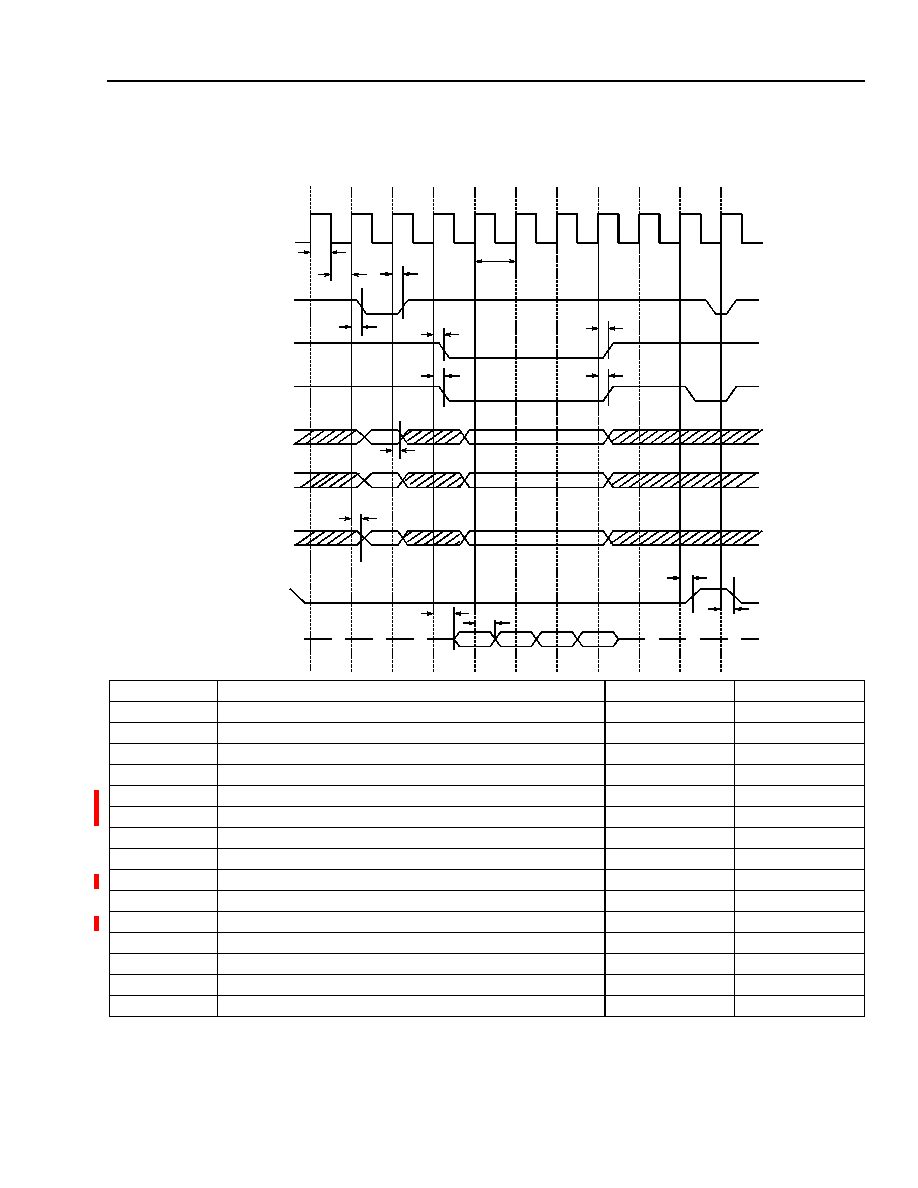
Agere Systems Inc.
93
Data Sheet
T8302 Internet Protocol Telephone
July 2001
Advanced RISC Machine (ARM )
8 External Memory Interface (EMI)
(continued)
Figure 15. SDRAM Write Timing Diagram
Reference
Parameter
Minimum
Maximum
t1
SDRCK High Time.
--
--
t2
SDRCK Low Time.
--
--
t3
SDRCK Cycle Times.
--
--
t4
SDRASN Output Delay.
--
7.25 ns
t5
SDRASN Output Hold Time.
6.98 ns
--
t6
Address/Precharge Output Hold Time.
7.28 ns
--
t7
Address/Precharge Maximum Output Delay Time.
--
7.44 ns
t8
SDCASN Maximum Output Delay.
--
7.27 ns
t9
SDCASN Output Hold Time.
7.14 ns
--
t10
SDWEN Maximum Output Delay.
--
7.31 ns
t11
SDWEN Output Hold Time.
7.11 ns
--
t12
Maximum Data Output Valid.
0 ns
--
t13
Minimum Data Hold Time.
1.90 ns
--
t14
Data I/O Mask Output Delay.
--
7.89 ns
t15
Minimum Data I/O Mask Output Hold Time.
--
7.09 ns
0
1
2
3
4
5
6
7
8
9
10
SDRASN
SDRCK
SDCASN
SDWEN
A[13:12]
BANK SELECT
A[10] AUTO
A[11:0]
SDLDQM/
SDUDQM
Ax0
Ax1
Ax2
Ax3
D[15:0]
BA
BANK SELECT
CAx
CAx
t1
t2
t4
t5
t8
t3
t9
t10
t11
t6
t7
t14
t15
t13
t12
PRECHARGE
BA
BA

94
Agere Systems Inc.
T8302 Internet Protocol Telephone
Data Sheet
Advanced RISC Machine (ARM )
July 2001
8 External Memory Interface (EMI)
(continued)
8.8 Signals
The EMI controls all the signals needed to access external devices. For transactions that are larger than the width
of the device, the EMI creates multiple accesses to read from or write to the device. For example, a 32-bit read from
an 8-bit device requires four read accesses. SDRAM, FLASH, and SRAMs share the same address and data bus.
8.8.1 Address, A[23:0]
For FLASH_CS, CS1, CS2, and CS3 devices, the address bus signals A[23:0] define the address of the least sig-
nificant byte transferred during a memory cycle. The address becomes valid during phase 1 of the first cycle of an
access and remains valid until phase 1 of first cycle of the next access.
Note: For FLASH and SRAM accesses, A[23:0] is used to access memory in units of bytes. If a 16-bit wide SRAM/
FLASH memory device is used, A[1] should be connected to the least significant address input pin of the
memory device. For 8-bit wide FLASH/SRAM devices, A[0] should be connected to the least significant
address input.
8.8.2 Data, D[15:0]
Data bus signals D[15:0] are bidirectional signals that transfer data to and from the chip. Use of the upper 8 bits of
the data bus is controlled on a per-device basis by BS (bit 6) of the chip select configuration register.
Note: The program memory that is accessed by FLASH_CS always uses a 16-bit data bus. During a read access,
the data on the data bus is latched at the end of phase 1 of the last active cycle of the access. For a write
access, the data becomes valid during phase 1 of the second cycle of the access. If there is no valid transac-
tion on the EMI, the data bus stays in input mode.
8.8.3 Byte Enable, BE1N
BE1N is used as a byte write enable for 16-bit devices that use byte enables. This signal is active-low and goes
active when an odd byte is to be written. The UBE bit (bit 13) of the chip select configuration register must be
set to 1 before attempting byte writes to 16-bit devices.
8.8.4 Read/Write Signals, RDN, WRN
RDN and WRN are active-low signals that indicate whether a read or a write access is taking place. During a read
access, RDN goes low and WRN stays high. During a write access, RDN stays high am WRN goes low. If the EMI
flash is not being accessed, RDN and WRN stay high.
8.8.5 Chip Selects, FLASH_CS, CS1, CS2, CS3
The chip select signals FLASH_CS, CS1, CS2, and CS3 indicate which of the external devices is accessed. The
appropriate chip select becomes active during phase 1 of the first cycle of an access if no setup cycle is used and
goes inactive after the last active cycle of the access. FLASH_CS is active-low. CS1, CS2, and CS3 have program-
mable polarities and are active-low at reset.
8.8.6 External WAIT, EXWAIT
This signal can be driven by the external device to add additional wait-states to the memory access cycle, if
required. The use of the EXWAIT signal by a particular device is enabled by setting the WT bit (bit 8) of the appro-
priate chip select configuration register. The polarity of EXWAIT is programmable, and is determined by the WP
bit (bit 0) of the options register;
see Table 65 on page 89
.

Agere Systems Inc.
95
Data Sheet
T8302 Internet Protocol Telephone
July 2001
Advanced RISC Machine (ARM )
8 External Memory Interface (EMI)
(continued)
8.8.7 EMI SDRAM, Synchronous DRAM Memory Interface
The EMI SDRAM interface can support one 16-bit wide synchronous DRAM device. SDRAM devices of other
widths (8-bit/4-bit) are not supported. Device sizes up to 256 Mbits are supported. The SDRAM's chip select
should be tied off to active.
8.8.8 SDRAM Address Functionality
Pins A[14:0] are used to output the row/column/bank address of the SDRAM location being accessed. Pins
A[23:15] are not used during an SDRAM access. The output on these pins depends upon the type of SDRAM
access cycle, e.g., when used with a 64 Mbit 16-bit wide SDRAM device.
8.8.9 SDRAM Clock, SDRCK
This is the clock output that should be connected to the SDRAM. This runs at the same frequency as the IPT_ARM
system clock.
8.8.10 SDRASN, SDCASN, SDWEN
SDRAM row address strobe (SDRASN), column address strobe (SDCASN), and write enable (SDWEN) are stan-
dard SDRAM interface signals. The combination of these three outputs is used to indicate the type of command
that is to be performed on SDRAM.
8.8.11 SDUDQM, SDLDQM
SDUDQM and SDLDQM are SDRAM upper byte enable and lower data byte enable, respectively. In read mode
SDUDQM/SDLDQM go low to turn on the SDRAM's output buffers. In write mode, SDUDQM/SDLDQM go low to
allow the corresponding byte to be written.
Note: Care should be taken to have the shortest possible routes on the board, and to avoid excessive loading
(>15 pF) for all the EMI pins.
Table 71. SDRAM Access Cycles, Using a 64 Mbit SDRAM
SDRAM Command Cycle
Address Pins
Row address strobe (RAS)
A[13: 0] = row address, where A[13:12] = bank select.
Column address strobe (CAS)
A[7:0] = column address.
Precharge
A[10] = precharge mode.
If A[10] = 1, all banks are precharged.
If A[10] = 0, only the bank selected by the bank select signals on the
SDRAM are precharged.

96
Agere Systems Inc.
T8302 Internet Protocol Telephone
Data Sheet
Advanced RISC Machine (ARM )
July 2001
9 DSP Communications Controller (DCC)
The DSP communications controller consists of the following elements:
s
ARM (write only) DSP (read-only) 512 x 32 bit internal SRAM for use as a communications mailbox.
s
ARM (read-only) DSP (write only) 512 x 32 bit internal SRAM for use as a communications mailbox.
s
Token register to support single owner of memory segments or message headers.
s
ARM 2DSP interrupt register.
s
DSP2ARM interrupt register.
s
Dedicated I/O pins for single wait-state DSP accesses.
s
DSP communications controller address map.
s
IPT_ARM peripheral controller circuits.
5-9379 (F)
Figure 16. DSP Communications Controller Block Diagram
9.1 ARM Processor Memory and I/O Map
Table 72. ARM Processor Memory and I/O Map
Register
Address
Token register
(see Table 73 on page 97)
.
0xE000 F000
Reserved.
0xE000 F004:0xE000 F01C
DSP2ARM interrupt register
(see Table 74 on page 98)
.
0xE000 F020
Reserved.
0xE000 F024:0xE000 F02C
ARM 2DSP interrupt register
(see Table 75 on page 98)
.
0xE000 F030
Reserved.
0xE000 F034:0xE000 F03C
ARM 2DSP data buffer; write only by ARM, read-only by DSP.
0xE004 0000:0xE004 07FF
Reserved.
0xE004 0800:0xE005 FFFF
DSP2ARM data buffer; write only by DSP, read-only by ARM.
0xE006 0000:0xE006 07FF
IPT_DSP
INTERFACE
APB
APB
INTERFACE
DSP_A[10:0]
DSP_D[15:0]
DSP_RWN
DSP_MCSN
ARM2DSP
BUFFER
INTERRUPT
AND
(512x32)
DSP2ARM
BUFFER
(512x32)
TOKEN
REGISTERS
TO INTERRUPT CONTROLLER
IRQ_DCC
(PERIPHERAL BUS)
DSP_ICSN

Agere Systems Inc.
97
Data Sheet
T8302 Internet Protocol Telephone
July 2001
Advanced RISC Machine (ARM )
9 DSP Communications Controller (DCC)
(continued)
9.2 DCC Token Register
The DSP communications controller (DCC) provides a 16-bit token register
(see Table 73 on page 97)
. The upper
byte (DSPT) of this register is writable only through the DSP interface. The lower byte (ARMT) of this register is
writable only through the ARM APB bus. The entire 16-bit token register can be read by either interface.
The token register should help the programmer manage the communication buffers. A jitter buffer, for example,
can be implemented by using the token bits to mark full areas and empty sections of the buffer. When an audio
packet is placed in the buffer by the IPT_ARM, it could interrupt the DSP with information about the section where
this packet was placed. The DSP could then use one of its token bits to mark that section as full. At the appropriate
time, the DSP could then remove a packet that was placed in its buffer many milliseconds earlier and mark this
other section as empty.
Table 73. Token Register
9.3 DCC Interrupt Registers
There are two DCC interrupt registers in the IPT_ARM. The DSP2ARM interrupt register
(see Table 74 on page
98)
is used by an external device (the IPT_DSP) to generate an interrupt to the ARM 940T processor core. The
ARM 2DSP interrupt register
(see Table 75 on page 98)
is written by the ARM 940T processor to generate an
active-low interrupt output. This interrupt output is to be connected to the IPT_DSP interrupt input (DSP_INT0).
Both of these registers are similarly organized. Bit 15, the MSB, is the interrupt bit and can only be written to 1 by
the interrupting processor. Bit 15 (DSP2ARM_INT) in the DSP2ARM interrupt register can only be set by the
external DSP through the DCC interface. Bit 15 (ARM 2DSP_INT) in the ARM 2DSP interrupt register can only
be set by the IPT_ARM processor. DSP2ARM_INT and ARM 2DSP_INT can read by both processors.
When bit 15 is set to 1 by the appropriate processor, INT_CLR and INT_FLAG are automatically set to 1. These
bits can only be written to 0 by the interrupted processor. When the interrupted processor writes INT_CLR to 0, bit
15 is automatically reset to 0 and clears the interrupt. In addition the interrupted processor can write INT_FLAG to
0 to indicate that it has completed the operation, or freed up the memory.
Bits 12:0 (INT_MSG) of the ARM 2DSP interrupt register
(see Table 75 on page 98)
can only be written by the
interrupting processor, which uses these bits to implement a message-passing protocol to signal the purpose of
the interrupt. These bits can also be used to identify an offset and length in the interprocessor communication buff-
ers where a message, or data, is stored.
This message-interrupt scheme should help the programmers pass data and commands back and forth while pre-
venting a processor from overwriting a set of data in the interprocessor communications buffer before the other
processor has finished accessing it.
Address 0xE000 F000
Bit #
31:16
15:8
7:0
Name
RSVD
DSPT
ARMT
Bit #
Name
Description
31:16
RSVD
Reserved.
15:8
DSPT
DSP writable token bits. These bits can only be written through the DSP interface but
they are readable by both the DSP and the ARM.
7:0
ARMT
ARM writable token bit. These bits can only be written by the ARM processor but they are
readable by both the DSP and the ARM.

98
Agere Systems Inc.
T8302 Internet Protocol Telephone
Data Sheet
Advanced RISC Machine (ARM )
July 2001
9 DSP Communications Controller (DCC)
(continued)
9.3.1 DSP2ARM Interrupt Register
Table 74. DSP2ARM Interrupt Register
9.3.2 ARM 2DSP Interrupt Register
Table 75. ARM 2DSP Interrupt Register
Address 0xE000 F020
Bit #
31:16
15
14
13
12:0
Name
RSVD
DSP2ARM_INT
INT_CLR
INT_FLAG
INT_MSG
Bit #
Name
Description
31:16
RSVD
Reserved.
15
DSP2ARM_INT DSP to ARM interrupt. Interrupt from the DSP to the ARM.
14
INT_CLR
Interrupt clear. This will clear the interrupt signal.
This is controlled only by the ARM.
13
INT_FLAG
Interrupt flag. Interrupt flag to signal to the DSP that an interrupt was serviced and
completed.
This is read-only from the DSP.
12:0
INT_MSG
Interrupt message. Interrupt message from the DSP.
This is read-only from the ARM.
Address 0xE000 F030
Bit #
31:14
15
14
13
12:0
Name
RSVD
ARM2DSP_INT
INT_CLR
INT_FLAG
INT_MSG
Bit #
Name
Description
31:14
RSVD
Reserved.
15
ARM 2DSP_INT ARM to DSP interrupt. Interrupt from the ARM to the DSP.
14
INT_CLR
Interrupt clear. Interrupt clear will clear the interrupt signal.
This is controlled only by the DSP.
13
INT_FLAG
Interrupt flag. Interrupt flag to signal to DSP that interrupt was serviced and com-
pleted.
This is read-only from the ARM.
12:0
INT_MSG
Interrupt message. Interrupt message from the ARM.
This is read-only from the DSP.

Agere Systems Inc.
99
Data Sheet
T8302 Internet Protocol Telephone
July 2001
Advanced RISC Machine (ARM )
9 DSP Communications Controller (DCC)
(continued)
9.4 DCC Controller I/O Signals
The DCC controller has several I/O signals used to support interprocessor communications.
9.5 DSP Read/Write Timing Diagrams
Figure 17. DSP Read Interface Timing Diagram
Table 76. DCC Controller I/O Signals
Signal
Description
DSP_A[10:0]
DSP address input signals[10:0]. Used to address the 1 Kword interprocessor memories,
tokens, or interrupt registers.
DSP_D[15:0]
DSP data bus[15:0]. This is the interprocessor data bus.
DSP_RWN
DSP read/write not strobe.
DSP_MCSN
DSP chip select. Used to indicate a DSP access of the buffer memories.
If A[10] is low the ARM to DSP memory is accessed.
If [A10] is high the DSP to ARM memory is accessed.
DSP_ICSN
DSP chip select. Used to indicate an access of the token or interrupt registers.
If A[3] = 0 then it is a token register access.
If A[3], A[2] = 10 then it is an ARM interrupt register access.
If A[3], A[2] = 11 then it is a DSP interrupt register access.
DSP_INTN0
DSP interrupt. Indicates an external interrupt signal to the DSP from the ARM processor.
Symbol
Description
Minimum
Maximum
t1
DSP_A setup to CSN active.
0 ns
--
t2
CSN active to DSP_D valid.
--
14.0 ns
t3
DSP_A hold after CSN inactive.
0 ns
--
t4
DSP_D high-impedance after CSN inactive.
--
9.0 ns
t5
CSN active time.
15.0 ns
--
t6
CSN inactive before successive reads.
10.0 ns
--
t2
t3
t1
DSP_A
DSP_RWN
DSP_D
t5
t4
t6
DSP_MCSN/
DSP_ICSN

100
Agere Systems Inc.
T8302 Internet Protocol Telephone
Data Sheet
Advanced RISC Machine (ARM )
July 2001
9 DSP Communications Controller (DCC)
(continued)
* This value depends on the number of wait-states programmed into T8301 (N) and the clock period of the T8301 clock (T) as follows:
t3 = N x T/2 + wire delay.
t7 = (2N + 1) x T/2.
For N = 2 and T = 12.5 ns (f = 80 MHz), t3 = 12.5 ns, t7 = 31.25 ns, t8 = 12.5 ns.
Figure 18. DSP Write Interface Timing Diagram
Symbol
Description
Minimum
Maximum
t1
DSP_A setup to CSN active.
0 ns
--
t2
CSN setup to RWN active.
0 ns
--
t3
DSP_D delay from RWN active.
--
13.00 ns*
t4
CSN hold from RWN inactive.
0 ns
--
t5
DSP_A hold from CSN inactive.
0 ns
--
t6
DSP_D hold from RWN inactive.
--
--
t7
RWN active time.
31.25 ns*
--
t8
RWN inactive between successive writes.
12.5 ns
--
DSP_A
DSP_RWN
DSP_D
t1
t7
t4
t2
t3
t5
t6
t8
DSP_MCSN/
DSP_ICSN
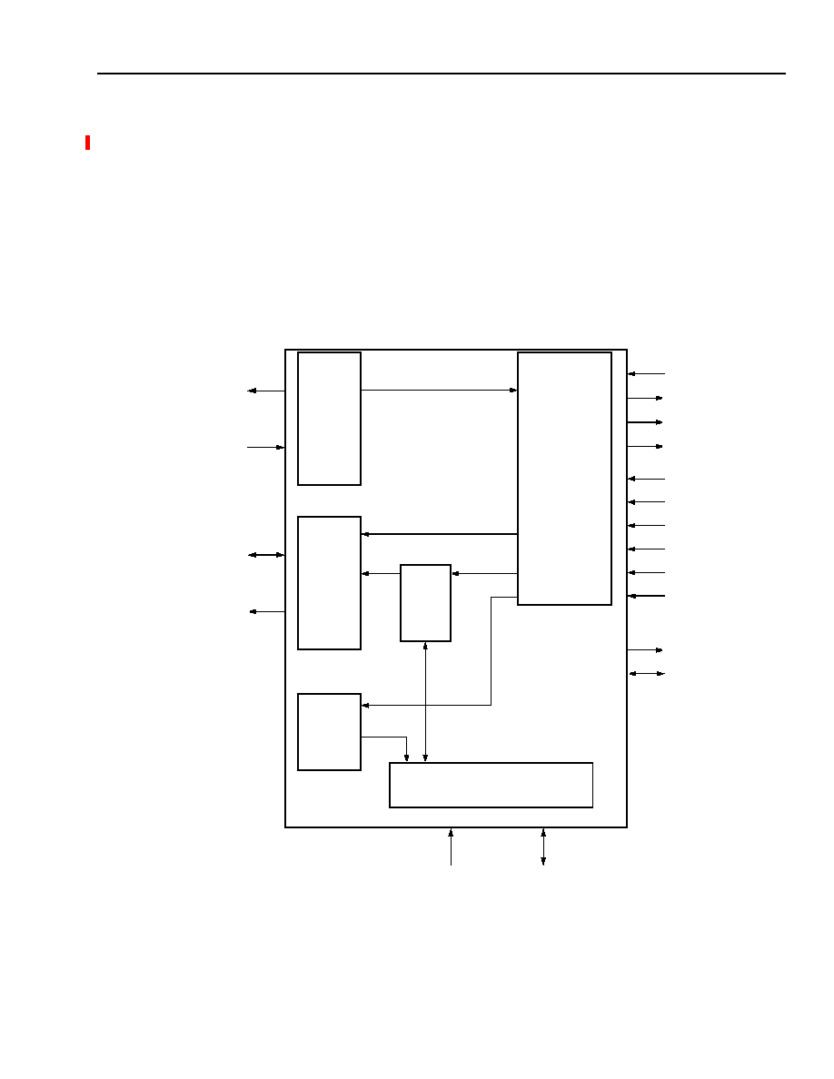
Agere Systems Inc.
101
Data Sheet
T8302 Internet Protocol Telephone
July 2001
Advanced RISC Machine (ARM )
10 Ethernet 10/100 MAC
Please refer to
Agere's
DNCM01 10/100 Ethernet MAC ASIC Macrocell Data Sheet for references.
All the registers inside the MAC controller are read/write through the ARM AMBA peripheral bus interface.
The IPT_ARM contains a 10/100 media access controller (MAC) and the logic to completely control packet trans-
mission and reception with minimal setup and intervention from the ARM 940T processor. The registers and logic
that control the operation of the MAC are referred to in this document as the MAC controller. The MAC provides the
timing and control for transmission and reception of packet bytes on the media through the PHY interfaces. It auto-
matically provides interframe timing, preamble, collision detect, media jam, and CRC (circular redundancy check-
sum) generation and detection. The MAC controller provides registers for MAC setup and control, 32 x 32 bit
FIFOs for receive and transmit data buffering, logic to sequence the 32-bit words into the MAC (8 bits at a time),
address matching on received packets, byte counters, and status bits.
Figure 19. Ethernet 10/100 MAC Block Diagram
RX
FIFO
RX
CONTROL
FIFO
TX
FIFO
CAM
APB REGISTER INTERFACE
MAC
CORE
ADDRESS
DATA
STATUS
DATA
RX DATA
TX DATA
TX_CLK
TX_ERR
TX_EN
TXD[3:0]
COL
RX_CLK
RXD[3:0]
CRS
RX_DV
RX_ERR
MDC
MDIO
RXD[3:0]
TX_DMA_RDY
DATA
RX_DMA_RDY
ADDRESS

102
Agere Systems Inc.
T8302 Internet Protocol Telephone
Data Sheet
Advanced RISC Machine (ARM )
July 2001
10 Ethernet 10/100 MAC
(continued)
10.1 Features
The Ethernet 10/100 MAC provides the following features:
s
Compliant with ISO* 8802.3 1993, IEEE
802.3u 1995, and IEEE 802.3x 1995 standards for media access con-
trol.
s
Data transmission and reception rates of 10 Mbits/s at a clock speed of 2.5 MHz or 100 Mbits/s at a clock speed
of 25 MHz.
s
Transmits or receives at full- or half-duplex.
s
Supports flow control.
s
Supports both VLAN type1 and VLAN type2 frame recognition.
s
Extensive network management signals are provided.
s
Transmit and receive functions can be asynchronously reset with no clocks present.
s
Supports full internal scan test methodology.
s
Retransmit capability on early collision detection.
s
Flexible arithmetic or logical physical address matching.
s
Queued storage of packet reception status and byte counts for relaxed real-time interrupt latency requirements.
s
128 bytes of FIFO buffering in both the transmit and receive directions.
s
Easy setup of control or pause frame transmission for network control.
10.2 General MAC Information
The IPT_ARM contains an AMBA peripheral bus interface (APB) to the status and control registers contained in
the MAC controller. This interface also has a reset signal that will reset the state machines, counters, and critical
logic in the MAC and its controller.
The MAC contains the MAC transmit status register, the MAC collision counter, and the MAC control frame
registers. The MAC transmit status register
(see Table 96 on page 116)
provides access to output signals that
describe the results of the last transmitted or received frame. The MAC collision counter
(see Table 97 on page
118)
is a 16-bit counter that reports the number of collisions on a transmit attempt. Valid counts are 0 through 15.
When the number of collisions is equal to the retry attempt value, RETRY[1:0], an excessive collision error occurs.
The MAC collision counter is cleared before each new packet transmission.The MAC control frame registers hold
the reserved multicast destination address, source address, reserved length/type field, control opcode, and data.
Flow control is implemented by receiving and sending pause (control) frames. The MAC handles the transfer of
data from the control registers to the transmit data bus of the MAC.
* ISO is a registered trademark of the International Organization for Standardization.
IEEE is a registered trademark of the Institute of Electrical and Electronics Engineers, Inc.

Agere Systems Inc.
103
Data Sheet
T8302 Internet Protocol Telephone
July 2001
Advanced RISC Machine (ARM )
10 Ethernet 10/100 MAC
(continued)
10.3 MAC Transmitter
The transmit path consists of a 32x32 FIFO and transmit state machine.The programmer initiates a packet trans-
mission by first setting up the DMA to transfer packet data from memory to the transmit FIFO, excluding the pream-
ble, SFD, and CRC. The START bit
(see Table 95 on page 116)
is asserted and packet byte count is loaded into the
MAC controller transmit start register
(see Table 95 on page 116)
. It is the responsibility of the host system to
keep the transmit FIFO from underrunning.
In half-duplex mode, the MAC handles the collisions in accordance with IEEE 802.3u. The MAC controller pre-
serves the first 64 bytes of data in the transmit FIFO so that, if there is a collision during the transmission of these
bytes, the MAC can retransmit the frame without the host system having to reload the FIFO. If a collision occurs
after 64 bytes have been transmitted, the transmission is aborted due to a late collision and an interrupt is gener-
ated if it is not masked.
The CRC is automatically appended at the end of the data packet and transmitted. An interrupt will be generated at
the end of a packet transmission to notify the processor about the successful or unsuccessful packet transmission.
If the interrupt is masked, then the host should monitor the MAC transmit status register
(see Table 96 on page
116)
to determine when the transmitter is finished with the packet transmission.
10.4 MAC Receiver
The programmer sets up the IPT_ARM to receive Ethernet packets by programming the MAC controller setup
register
(see Table 78 on page 106)
and address matching registers to determine which packets to accept and to
set up the circular input buffer in the IPT_ARM DMA block. If the receiver is enabled the incoming packets are
accepted and stored if they match the receive criteria.
The MAC can operate in a hardware flow control environment. When operating in full-duplex mode, if a pause
frame is received, the MAC controller waits for the time the sender wishes the MAC not to transmit. In addition, the
MAC controller also monitors the presence of VLAN type1 and type2 fields. If one of them is present, the maximum
legal frame length is extended.
An interrupt will be generated (if enabled) on a successful or unsuccessful packet reception and the status and
byte count of the received packet will be placed in the receive control FIFO. This information can be used by the
programmer to determine the amount of data written into the DMA input circular buffer and to determine the validity
of this data.
10.4.1 Address Matching Registers
The IPT_ARM has the capability of storing only those packets that meet predefined destination address criteria
programmed in 32 pairs of address match memory locations. Address match memory location 0 (memory loca-
tions 0XE001 0B00 and 0XE001 0B04) should be programmed with the endpoint's MAC address (the low-order 32
bits of the MAC address go in 0XE001 0B00 and the high-order 16 bits go in the least significant 16 bits of
0XE001 0B04). When the MAC receiver is not in promiscuous mode (PROMM = 0), received unicast packets will
only be written to the MAC receive FIFO if their destination addresses match the 48-bit value stored in address
match memory location 0.
Address match memory locations 1 to 31 (locations 0XE001 0B08 to 0XE001 0BFC) can be used to store up to
31 multicast addresses. These locations are paired in the same way that address match memory location 1 is; the
low-order 32 bits of the multicast address go in the first memory location of the pair and the high-order 16 bits go in
the least significant 16 bits of the second memory location of the pair. When the MAC receiver is not in the store-all
multicast packets mode (SAMUL = 0,
see Table 78 on page 106
), received multicast packets will only be written to
the MAC receive FIFO if their destination addresses match one of the thirty-one 48-bit values.

104
Agere Systems Inc.
T8302 Internet Protocol Telephone
Data Sheet
Advanced RISC Machine (ARM )
July 2001
10 Ethernet 10/100 MAC
(continued)
10.5 MAC Controller, Registers, and Counters
There are several registers and counters in the MAC controller. The registers include control setup registers,
control registers, and status registers. There are thirty-two 48-bit address matching registers that are used to
determine whether received multicast packets are stored. Location 0 in the address match memory registers is
always reserved for the MAC's physical address. The remaining registers are used to store multicast addresses
that are compared against received packet destination addresses. If there is a match, the packet is stored.
If store-all multicast packets mode is selected (SAMUL set to 1 in the MAC controller setup register;
see Table
78 on page 106
) all multicast packets will be stored without regard to values in the address match registers. If
promiscuous mode is selected (PROMM set to 1 in the MAC controller setup register), all packets are stored (no
address matching is performed).
The counters are used to control the MDIO interface to the PHYs, assemble and send pause control frames, and
recognize VLAN packets.
10.6 Control Frame Operation
The MAC supports control frame transmission and automatic pause control frame response for use in flow-control
of full-duplex networks. In the transmit direction, the MAC can transmit control frames to the far end without having
to go through the process of writing to the transmit FIFO. This is done by programming register addresses
0XE001 000C to 0XE001 002C with the control frame information and then setting the CNTLXMIT bit (in the MAC
controller transmit control register) to initiate transmission.
In the receive direction, the MAC will respond to the reception of pause commands by pausing the MAC transmitter
for the requested number of bit times. To enable this automatic pause response, register addresses
0XE001 000C to 0XE001 0028 must be programmed with the proper values for a pause command.
See
Table 81
--
Table 85
for more information.

Agere Systems Inc.
105
Data Sheet
T8302 Internet Protocol Telephone
July 2001
Advanced RISC Machine (ARM )
10 Ethernet 10/100 MAC
(continued)
* Read-only latch, ROL. A read-only latch is similar to a read-only field (RO), except that once it is set, it stays set regardless of the state of any
event that set it in the first place. It can only be reset by the microprocessor writing a 1 to the bit. Note that the microprocessor writing a 0 to an
ROL has no effect at all.
Table 77. MAC Register Map
Description
Address
R/W
MAC controller setup register
(see Table 78 on page 106)
.
0xE001 0000
R/W
MAC packet delay alarm value
(see Table 79 on page 108)
.
0xE001 0004
R/W
MAC controller interrupt enable register
(see Table 80 on page 108)
.
0xE001 0008
R/W
MAC control frame destination address register
(see Table 81 on page
109)
.
0xE001 000C:0xE001 0014
R/W
MAC control frame source address registers
(see Table 82 on page 109)
. 0xE001 0018:0xE001 0020
R/W
MAC control frame length/type register
(see Table 83 on page 110)
.
0xE001 0024
R/W
MAC control frame opcode register
(see Table 84 on page 110)
.
0xE001 0028
R/W
MAC control frame data register
(see Table 85 on page 111)
.
0xE001 002C
R/W
VLAN type1 type/length field register
(see Table 86 on page 111)
.
0xE001 0030
R/W
VLAN type2 type/length field register
(see Table 87 on page 111)
.
0xE001 0034
R/W
MAC transmit FIFO register
(see Table 88 on page 111)
.
0xE001 0038
W
MAC receive FIFO register
(see Table 89 on page 112)
.
0xE001 003C
R
MAC receive control FIFO register
(see Table 90 on page 112).
0xE001 0040
R
MDIO address register
(see Table 91 on page 114)
.
0xE001 0044
R/W
MDIO data register
(see Table 92 on page 114)
.
0xE001 0048
R/W
Reserved.
0xE001 004C:0xE001 01FC
--
PHY powerdown register
(see Table 93 on page 115)
.
0xE001 0200
R/W
Reserved.
0xE001 0204:0xE001 07FC
--
MAC controller transmit control register
(see Table 94 on page 115)
.
0xE001 0800
R/W
MAC controller transmit start register
(see Table 95 on page 116)
.
0xE001 0804
R/W
MAC transmit status register
(see Table 96 on page 116)
.
0xE001 0808
R
MAC collision counter
(see Table 97 on page 118)
.
0xE001 080C
R
MAC packet delay counter
(see Table 98 on page 118)
.
0xE001 0810
R
MAC transmitted packet counter
(see Table 99 on page 118)
.
0xE001 0814
R/W
MAC transmitted single collision counter
(see Table 100 on page 118)
.
0xE001 0818
R/W
MAC transmitted multiple collision counter
(see Table 101 on page 119)
.
0xE001 081C
R/W
MAC excess collision counter
(see Table 102 on page 119)
.
0xE001 0820
R/W
MAC packet deferred counter
(see Table 103 on page 119)
.
0xE001 0824
R/W
Reserved.
0xE001 0828:0xE001 09FC
--
MAC controller receive control register
(see Table 104 on page 119)
.
0xE001 0A00
R/W
Reserved.
0xE001 0A04:0xE001 0AFC
--
Address match memory location 0--low-order 32 bits (physical address).
0xE001 0B00
R/W
Address match memory location 0--high-order 16 bits (physical address).
0xE001 0B04
R/W
Address match memory locations 1 through 31
(multicast address).
These locations are arranged in pairs in the same manner as address match
memory location 0. The first memory location of each pair holds the low-
order 32 bits of the multicast address, and the second least significant 16
bits hold the high-order 16 bits of the multicast address.
0xE001 0B08:0xE001 0BFC
R/W
MAC FIFO status register
(see Table 105 on page 120)
.
0xE001 0C00
R
MAC controller interrupt status register
(see Table 106 on page 120)
.
0xE001 0C04
RO/
ROL*

106
Agere Systems Inc.
T8302 Internet Protocol Telephone
Data Sheet
Advanced RISC Machine (ARM )
July 2001
10 Ethernet 10/100 MAC
(continued)
10.7 Register Descriptions
10.7.1 MAC Controller Setup Register
The MAC controller setup register is used to set up MAC control bits. The transmit and receive state machines
are reset with the appropriate reset bits. The transmit and receive enable bits must be set for the MAC controller to
send or receive data from the MAC and FIFOs.
Table 78. MAC Controller Setup Register
Address 0xE001 0000
Bit #
15:14
13
12
11
10
9
8
Name
SPEED_SEL
SBCSTP
SAMUL
PROMM
TMODE
INVCRC
BSEL
Bit #
7
6
5
4
3:2
1:0
--
Name
DEFER
ISQE
MFDUP
APDCRC
RETRY[1:0]
PREAMBLE[1:0]
--
Bit #
Name
Description
15:14
SPEED_SEL MDC rate of PCLK (system clock). MDC is the management data clock for the PHYs. The
MDC rate must be kept below 6.25 MHz, therefore, SPEED_SEL should be programmed
accordingly. For example: if PCLK is 57 MHz, MDC = PCLK/8 = 7.125 MHz,
(SPEED_SEL = 11) is an invalid setting and SPEED_SEL = 00, 01 or 10 should be used.
00
MDC = PCLK/64
01
MDC = PCLK/32
10
MDC = PCLK/16
11
MDC = PCLK/8
13
SBCSTP
Store broadcast packets.
If 1, all broadcast packets are stored.
If 0, no broadcast packets are stored.
12
SAMUL
Store all multicast packets. Indicates that all multicast packets should be stored.
11
PROMM
Promiscuous mode. When 1, this indicates all packets should be received without
address matching.
10
TMODE
Reserved for factory testing. This should be programmed to 0.
9
INVCRC
Invert CRC (active-high)
.
Used to invert the polarity of the 32-bit CRC polynomial.
The
nor-
mal CRC is inverted prior to transmission.
If INVCRC is high, the normal CRC is reinverted prior to sending, forcing a CRC error.
8
BSEL
Backoff select (active-low). Used to control whether the binary backoff algorithm is used
during collision handling.
If BSEL is high, the backoff algorithm is not used. The transmitter jams for 32 TX_CLK
cycles and attempts to retransmit after 96 bit times (normal IFG).
If BSEL is low, the transmitter follows the normal binary backoff algorithm following a col-
lision.
7
DEFER
Defer (active-high). Used to force the transmitter to abort a transmission attempt if it has
deferred for more than 24,288 TX_CLK cycles. Deferring starts when the transmitter is
ready to transmit, but is prevented from doing so because CRS is active. Defer time is not
cumulative. If the transmitter defers for 10,000 bit times, then transmits, collides, backs off,
and then has to defer again after completion of backoff, the deferral timer resets to 0 and
restarts.
If DEFER is low, the transmitter defers indefinitely.

Agere Systems Inc.
107
Data Sheet
T8302 Internet Protocol Telephone
July 2001
Advanced RISC Machine (ARM )
10 Ethernet 10/100 MAC
(continued)
Table 78. MAC Controller Setup Register (continued)
Bit #
Name
Description
6
ISQE
Ignore SQE test. Used to ignore the SQE signal from the PHY during the first 64 bit
times of interframe gap.
If high, the SQE error flag will not be set.
5
MFDUP
MAC full duplex (active-high). Used to control half- or full-duplex operation.
When MFDUP is low, the COL input is monitored and the binary backoff algorithm is
employed if collisions occur during transmission.
When MFDUP is low and CRS is asserted while the MAC's own packet is being trans-
mitted, the receiver is not enabled since the received packet is the MAC's own transmit-
ted packet.
When MFDUP is high, all packets are received regardless of the status of the transmit-
ter.
4
APDCRC
Append CRC (active-high). Used to control if a 32-bit CRC polynomial is appended to
the end of transmitted packet.
If high, the CRC is appended.
3:2
RETRY[1:0]
Retry. Used to control the total number of attempts (initial + retries after collision) the
MAC makes to transmit a packet. The total attempts follow the table below:
RETRY1
RETRY0 ATTEMPTS
0
0
16
0
1
8
1
0
4
1
1
1
1:0
PREAMBLE[1:0] Preamble. Used to control the number of preamble bits that will be transmitted before
the start of frame delimiter.
PREAMBLE1 PREAMBLE0 PREAMBLE
0
0
56 bits
0
1
48 bits
1
0
40 bits
1
1
8 bits

108
Agere Systems Inc.
T8302 Internet Protocol Telephone
Data Sheet
Advanced RISC Machine (ARM )
July 2001
10 Ethernet 10/100 MAC
(continued)
10.7.2 MAC Packet Delay Alarm Value Register
Table 79. MAC Packet Delay Alarm Value Register
10.7.3 MAC Controller Interrupt Enable Register
Table 80. MAC Controller Interrupt Enable Register
Address 0xE001 0004
Bit #
31:0
Name
ALARMVALUE
Bit #
Name
Description
31:0
ALARMVALUE Alarm value. This 32-bit register is a late transmit limit value. If the packet delay count
value reaches this limit, the late packet bit is set in the MAC transmit status register
(see Table 96 on page 116)
if enabled in the MAC controller transmit control regis-
ter
(see Table 94 on page 115)
.
An interrupt will be generated when the late status bit is set, if enabled.
Address 0xE001 0008
Bit #
15
14
13
12
11
10
9
8
Name
RSGPI
RSBPI
RSVD
RSVD
DFOVR
CFOVR
CFF
CFNE
Bit #
7
6
5
4
3
2
1
0
Name
TGPI
RSVD
TPLI
ECI
LCI
EXDEFI
EXCOLI
DFUND
Bit #
Name
Description
15
RSGPI
Good packet interrupt enable. Received and stored good packet interrupt enable.
14
RSBPI
Bad packet interrupt enable. Received and stored bad packet interrupt enable.
13:12
RSVD
Reserved.
11
DFOVR
Data FIFO overflow. Receive data FIFO overflow interrupt enable.
10
CFOVR
Control FIFO overflow. Receive control FIFO overflow interrupt enable.
9
CFF
Control FIFO full. Receive control FIFO full interrupt enable.
8
CFNE
Control FIFO not empty. Receive control FIFO not empty.
7
TGPI
Transmitted good packet interrupt. Transmitted good packet interrupt enable.
6
RSVD
Reserved.
5
TPLI
Transmit packet late interrupt. Transmit packet late interrupt enable.
4
ECI
Early collision. Early collision detect interrupt enable.
3
LCI
Late collision. Late collision detect interrupt enable.
2
EXDEFI
Excess deferral. Excess deferral interrupt enable.
1
EXCOLI
Excess collision. Excess collision interrupt enable.
0
DFUND
Transmit data FIFO. Transmit data FIFO data underrun interrupt enable.

Agere Systems Inc.
109
Data Sheet
T8302 Internet Protocol Telephone
July 2001
Advanced RISC Machine (ARM )
10 Ethernet 10/100 MAC
(continued)
10.7.4 MAC Control Frame Destination Address Registers
Table 81. MAC Control Frame Destination Address Registers
10.7.5 MAC Control Frame Source Address Registers
Table 82. MAC Control Frame Source Address Registers
Addresses 0xE001 000C:0xE001 0014
Bit #
47:0
Name
CDEST
Bit #
Name
Description
47:0
CDEST
Control frame destination address. This is a 48-bit reserved multicast address register for
control frames.
When transmitting a MAC control frame, these bits will be used as the destination
address field of the outgoing frame. See the CNTLXMIT bit description in
Table 95 on
page 116
.
When receiving a MAC control frame, these bits will be compared against the destination
address field of the incoming frame. If the received frame is a pause control frame, the
IPT_ARM MAC will automatically pause transmitter activity for the required number of bit
times.
The required values for automatic pause response are:
0xE001 000C:0x0180
0xE001 0010:0xC200
0xE001 0014:0x0001
These bits are only valid for full-duplex mode.
Addresses 0xE001 0018:0xE001 0020
Bit #
47:0
Name
CSOURCE
Bit #
Name
Description
47:0
CSOURCE
Control frame source address. This is a 48-bit individual address register of the station
sending the frame.
When transmitting a MAC control frame, these bits will be used as the source address
field of the outgoing frame. See the CNTLXMIT bit description in
Table 95 on page 116
.

110
Agere Systems Inc.
T8302 Internet Protocol Telephone
Data Sheet
Advanced RISC Machine (ARM )
July 2001
10 Ethernet 10/100 MAC
(continued)
10.7.6 MAC Control Frame Length/Type Register
Table 83. MAC Control Frame Length/Type Register
10.7.7 MAC Control Frame Opcode Register
Table 84. MAC Control Frame Opcode Register
Address 0xE001 0024
Bit #
15:0
Name
CTYPE
Bit #
Name
Description
15:0
CTYPE
Control frame length/type. This is the assigned 2-octet length/type field of a MAC control
frame.
When transmitting a MAC control frame, these bits will be used as the length/type field of
the outgoing frame. See the CNTLXMIT bit description in
Table 95 on page 116
.
When receiving a MAC control frame, these bits will be compared against the length/type
field of the incoming frame. If the received frame is a pause control frame and these bits
have been programmed to the proper values for a pause frame, the IPT_ARM MAC will
automatically pause transmitter activity for the required number of bit times. The required
values for automatic pause response are: 0xE001 0024:0x8808.
Address 0xE001 0028
Bit #
15:0
Name
COPCODE
Bit #
Name
Description
15:0
COPCODE
Control frame opcode. This is the 2-octet MAC control opcode field indicating the MAC
control function.
When transmitting a MAC control frame, these bits will be used as the opcode field of the
outgoing frame. See the CNTLXMIT bit description in
Table 95 on page 116
.
When receiving a MAC control frame, these bits will be compared against the opcode field
of the incoming frame. If the received frame is a pause control frame and these bits have
been programmed to the proper values for a pause frame, the IPT_ARM MAC will automat-
ically pause transmitter activity for the required number of bit times. The required values for
automatic pause response are: 0xE001 0028:0x0001.

Agere Systems Inc.
111
Data Sheet
T8302 Internet Protocol Telephone
July 2001
Advanced RISC Machine (ARM )
10 Ethernet 10/100 MAC
(continued)
10.7.8 MAC Control Frame Data Register
Table 85. MAC Control Frame Data Register
10.7.9 VLAN Type1 Type/Length Field Register
Table 86. VLAN Type1 Type/Length Field Register
10.7.10 VLAN Type2 Type/Length Field Register
Table 87. VLAN Type2 Type/Length Field Register
10.7.11 MAC Transmit FIFO Register
Table 88. MAC Transmit FIFO Register
Address 0xE001 002C
Bit #
15:0
Name
CPARAM
Bit #
Name
Description
15:0
CPARAM
MAC control parameters. Two octets hold MAC control opcodes specific parameters.
When transmitting a MAC control frame, these bits will be used as the least significant two
bytes of the data field of the outgoing frame. See the CNTLXMIT bit description in
Table 95
on page 116
.
Address 0xE001 0030
Bit #
31:16
15:0
Name
RSVD
TYPE [15:0]
Bit #
Name
Description
31:16
RSVD
Reserved.
15:0
TYPE[15:0]
VLAN type1 (read/write). VLAN type1 type/length field value.
Address 0xE001 0034
Bit #
31:16
15:0
Name
RSVD
TYPE [15:0]
Bit #
Name
Description
31:16
RSVD
Reserved.
15:0
TYPE[15:0]
VLAN type2 (read/write). VLAN type2 type/length field value.
Address 0xE001 0038
Bit #
31:0
Name
DATA
Bit #
Name
Description
31:0
DATA
Data (Write only). 32-bit data written to this FIFO is transmitted out, LSB first.

112
Agere Systems Inc.
T8302 Internet Protocol Telephone
Data Sheet
Advanced RISC Machine (ARM )
July 2001
10 Ethernet 10/100 MAC
(continued)
10.7.12 MAC Receive FIFO Register
Table 89. MAC Receive FIFO Register
10.7.13 MAC Receive Control FIFO Register
This register is used to access the status words in the receive control FIFO. Each status word has the format
shown in Table 90.
Table 90. MAC Receive Control FIFO Register
Address 0xE001 003C
Bit #
31:0
Name
DATA
Bit #
Name
Description
31:0
DATA
Data (read-only). Data received into this register, LSB first.
Address 0xE001 0040
Bit #
31
30
29
28
27
26
Name
IFG
RXJAB
FAE
CRC
RUNT
FRAG
Bit #
25
24
23
22
21
20
Name
LONG
PHYS
MULT
BROAD
RCNTRL
RUNSUP
Bit #
19
18
17
16
15:0
--
Name
RPAUSE
RX_VLAN2
RX_VLAN1
RXEROUT
RXCOUNT
--
Bit #
Name
Description
31
IFG
Short IFG (active-high). Indicates that the interframe gap prior to the start of the packet was
less than 76 bit times.
Valid on the positive edge of RX_CLK.
30
RXJAB
Receive jabber error (active-high). Indicates that the receive packet length was greater than
1518 bytes, and that the packet had a bad CRC or FAE.
Valid on the positive edge of RX_CLK.
29
FAE
Frame alignment error (active-high). Indicates a packet was received with a frame alignment
error. An FAE occurs when the resultant remainder from the division between the number of
bits in a frame and eight is nonzero (nonintegral number of octets), the CRC is invalid, and
the octet counters are greater than or equal to 64 and less than or equal to 1518. Valid on
the positive edge of RX_CLK.
Dribble bits have no effect.
28
CRC
CRC error (active-high). Indicates a packet was received with a bit count having a mod 8
remainder equal to 0 (integral number of octets), and that the packet had an incorrect CRC.
Valid on the positive edge of RX_CLK.
27
RUNT
Runt packet (active-high). Indicates a packet was received with a byte count
(including CRC) <64, and the packet had a good CRC.
Valid on the positive edge of RX_CLK.
26
FRAG
Fragment (active-high). Indicates a packet was received with a byte count
(including CRC) <64, and the packet had a bad CRC or FAE.
Valid on the positive edge of RX_CLK.

Agere Systems Inc.
113
Data Sheet
T8302 Internet Protocol Telephone
July 2001
Advanced RISC Machine (ARM )
10 Ethernet 10/100 MAC
(continued)
Table 90. MAC Receive Control FIFO Register (continued)
Bit #
Name
Description
25
LONG
Frame long error (active-high). Indicates that the received packet's length was greater than
1518 bytes, and the packet had good CRC.
Valid on the positive edge of RX_CLK.
24
PHYS
Received physical address (active-high). Indicates that the first bit of the received packet
was 0, and that at least 6 bytes of data were received.
Valid on the positive edge of RX_CLK.
23
MULT
Received multicast address. Indicates that the first bit of the received packet was 1, all
address bits were not 1, and that at least 6 bytes of data were received.
Valid on the positive edge of RX_CLK.
22
BROAD
Received broadcast address. Indicates that all 48 address bits of a received frame are 1.
Valid on the positive edge of RX_CLK.
21
RCNTRL
MAC control frame received. Indicates that the last packet received was a valid MAC control
frame.
Valid on the positive edge of RX_CLK.
20
RUNSUP
Unsupported opcode received. Indicates that the last MAC control frame received had an
unsupported opcode.
Valid on the positive edge of RX_CLK.
19
RPAUSE
PAUSE frames received. Indicates that the last control frame received has a multicast
address, length/type field, and opcode for the pause operation.
Valid on the positive edge of RX_CLK.
18
RX_VLAN2 VLAN type2 frame. When this signal is set, the current reception is tagged with a VLAN
type2 ID. The thirteenth and fourteenth bytes at the frame are compared to the VLAN type2
type/length field register.
This signal is set if there is a nonzero match.
17
RX_VLAN1 VLAN type1 frame. When this signal is set, the current reception is tagged with a VLAN
type1 ID. The thirteenth and fourteenth bytes at the frame are compared to the VLAN type1
type/length field register.
This signal is set if there is a nonzero match.
16
RXEROUT Receive error output (active-high). Active from RXEOP of an incoming frame to RXSOP of
the next frame, synchronous with RXC. RXEOP can be used to strobe RXEROUT.
RXEROUT will activate if the RX_ERR input from the MII activates for one or more clocks
while RX_DV is high.
15:0
RXCOUNT Receive byte count. Receive byte count at end of packet.
Read-only.

114
Agere Systems Inc.
T8302 Internet Protocol Telephone
Data Sheet
Advanced RISC Machine (ARM )
July 2001
10 Ethernet 10/100 MAC
(continued)
10.7.14 MDIO Address Register
This register is written with the address of the PHY and a specific register within the PHY to initiate a PHY register
read or write operation.
Table 91. MDIO Address Register
10.7.15 MDIO Data Register
Table 92. MDIO Data Register
Address 0xE001 0044
Bit #
15
14
13
12
11
10
9
Name
PHY4
PHY3
PHY2
PHY1
PHY0
REG4
REG3
Bit #
8
7
6
5:2
1
0
--
Name
REG2
REG1
REG0
RSVD
WRITE
BUSY
--
Bit #
Name
Description
15:11
PHY[4:0]
PHY address. These bits tell which of the 32 possible PHY devices are being accessed.
10:6
REG[4:0]
MII register. These bits select the desired MII register in the selected PHY device.
5:2
RSVD
Reserved. These bits are reserved and must be set to 0.
1
WRITE
MII write. Setting this bit tells the PHY that this will be a write operation using the MII data
register. If this bit is not set, this will be a read operation, placing the data in the MII data
register.
0
BUSY
MII busy. This bit should read a logic 0 before writing to the MII address and MII data
registers. During a MII register access, this bit will then be set to signify that a read or
write is in progress. The MII data register should be kept valid until this bit is cleared
during a PHY write operation. The MII data register is invalid until this bit is cleared by
the MAC during a PHY read operation. The MII address register should not be written to
until this bit is cleared.
This bit is read-only.
Address 0xE001 0048
Bit #
15:0
Name
DATA 15:0
Bit #
Name
Description
15:0
DATA[15:0]
MDIO data. 16-bit data value read from the PHY after a MDIO read operation. 16-bit data
value to be written to the PHY before a MDIO write operation.

Agere Systems Inc.
115
Data Sheet
T8302 Internet Protocol Telephone
July 2001
Advanced RISC Machine (ARM )
10 Ethernet 10/100 MAC
(continued)
10.7.16 MAC PHY Powerdown Register
Table 93. MAC PHY Powerdown Register
10.7.17 MAC Controller Transmit Control Register
Table 94. MAC Controller Transmit Control Register
Address 0xE001 0200
Bit #
31:2
1
0
Name
RSVD
PHY1
PHY0
Bit #
Name
Description
31:2
RSVD
Reserved.
1
PHY1
PHY1. Read/write. If 1, power down.
Default = 1.
0
PHY0
PHY0. Read/write.
Default = 0.
Address 0xE001 0800
Bit #
15
14
5
4
3
2
1
0
Name
RXMT
RRND
TRME
TLME
CNTLXMIT
TXABORT
RESTARTFIFO
RSTFIFO
Bit #
Name
Description
15
RXMT
Reset transmit. Must be written to 0 before attempting to use transmitter.
14
RRND
Reset random counter (write 1, then write 0).
5
TRME
Transmitter enable. Set to 1 to enable transmission of packets.
4
TLME
Transmitter late mode enable. When set to 1, an internal late counter counts the
number of transmit clocks from transmit start until the packet is sent or transmission
is halted. If the late counter matches the late alarm value (ALARMVALUE;
see Table
79 on page 108
) an interrupt will be generated if enabled. This allows the processor
to know when real time packets are no longer meaningful due to excessive transmis-
sion delay.
3
CNTLXMIT
Control transmit request. When this bit is set, the MAC control frame programmed in
register addresses 0xE001 0014 to 0XE001 002C will be transmitted.
This bit is self-clearing.
2
TXABORT
Transmit abort (active-high). Used to stop a transmission ungracefully. The transmit-
ter immediately terminates a transmission if this input is set. TXABRT should be held
high for two or more TX_CLK cycles. When a packet is aborted during preamble, the
preamble is completed and the APNDCRC and INVCRC inputs are followed. If
TXABORT is activated during transmission, transmission immediately stops, and the
APNDCRC and INVCRC inputs are followed.
This bit is held high for two TX_CLK cycles, then self-clears.
1
RESTARTFIFO
Restart FIFO. This bit only resets the read pointer of the transmit FIFO.
0
RSTFIFO
Reset FIFO. This bit resets both the read and write pointers of the transmit FIFO.

116
Agere Systems Inc.
T8302 Internet Protocol Telephone
Data Sheet
Advanced RISC Machine (ARM )
July 2001
10 Ethernet 10/100 MAC
(continued)
10.7.18 MAC Controller Transmit Start Register
Table 95. MAC Controller Transmit Start Register
10.7.19 MAC Transmit Status Register
Table 96. MAC Transmit Status Register
Address 0xE001 0804
Bit #
15
14:0
Name
START
COUNT
Bit #
Name
Description
15
START
Start bit. The MAC controller starts attempting to transmit a packet when set. This bit is
reset by the MAC controller when packet transmission is terminated.
14:0
COUNT
Count value. The 15-bit value is the number of bytes to be transmitted, not including the
CRC.
Address 0xE001 0808
Bit #
15
14
13
12
11
10
9
8
Name
EXDEF
DEF
SCOL
MCOL
CERR
COLDET
LCRS
ABORTED
Bit #
7
6
5
4
3
2
1
0
Name
LATE
TCNTRL
SQEFAIL
PAUSEACTIVE
TX_VLAN2 TX_VLAN1
TXBROAD
TXMULT
Bit #
Name
Description
15
EXDEF
Excessive deferral (active-high). Indicates transmission ended because of waiting for
more than 24,288 bit times for the medium to become not busy.
Valid on the positive edge of TX_CLK. The assertion of this bit is temporary.
14
DEF
Deferral (active-high). Indicates that a transmission was deferred for one bit time to
24,288 bit times during transmission.
Valid on the positive edge of TX_CLK.
13
SCOL
Single collision (active-high). Indicates that there was one collision during transmission of
the previous packet.
Valid on the positive edge of TX_CLK.
12
MCOL
Multiple collisions (active-high). Indicates that there was more than one collision during
the transmission of the previous packet.
Valid on the positive edge of TX_CLK.
11
CERR
Collision error (active-high). Indicates that the previous transmission was stopped
because of excessive collisions as allowed by the RETRY[1:0] inputs. SCOL and MCOL
are also valid if CERR is active.
Valid on the positive edge of TX_CLK.
10
COLDET
Collision detected (active-high). Indicates that a collision has been detected. This signal is
active from the time of a collision until the completion of the 32-bit jam sequence. The
COL signal is monitored only when the transmitter is actively transmitting data. This signal
is temporary; it may not be held long.
Valid on the positive edge of TX_CLK.

Agere Systems Inc.
117
Data Sheet
T8302 Internet Protocol Telephone
July 2001
Advanced RISC Machine (ARM )
10 Ethernet 10/100 MAC
(continued)
Table 96. MAC Transmit Status Register (continued)
Bit #
Name
Description
9
LCRS
Loss of carrier (active-high). Indicates that the CRS input was inactive for one or more
bit times while the transmitter is active and in half-duplex.
Valid on the positive edge of TX_CLK.
8
ABORTED
Transmission aborted (active-high). Indicates that a transmission has been aborted
before completion. This signal is cleared prior to the start of the next packet.
Valid on the positive edge of TX_CLK.
7
LATE
Late collision (active-high). Indicates that a collision occurred more than 512 bit times
from the start of a transmission. The start of transmission is defined as the transmis-
sion of the first bit of preamble.
Valid on the positive edge of TX_CLK.
6
TCNTRL
MAC pause control frame transmitted. Indicates that the last packet sent was a MAC
pause control frame.
Valid on the positive edge of TX_CLK.
5
SQEFAIL
SQE test failed (active-high).
Indicates that a COL signal was not detected during the
first 6.4
µ
s of interframe gap following a transmit attempt. SQE is inactive if the ISQE
input is high. This signal is only useful during test.
Valid on the positive edge of TX_CLK.
4
PAUSEACTIVE
Pause active (active-high).
Active while the transmitter is blocked from transmitting
after the reception of a pause command.
This output is synchronous with TXC.
3
TX_VLAN2
VLAN type2 frame. When this signal is set, the current transmission is tagged with a
VLAN type2 ID. The thirteenth and fourteenth bytes at the frame are compared to the
VLAN type2 type/length field register.
This signal is set if there is a nonzero match.
2
TX_VLAN1
VLAN type1 frame. When this signal is set, the current transmission is tagged with a
VLAN type1 ID. The thirteenth and fourteenth bytes at the frame are compared to the
VLAN type1 type/length field register.
This signal is set if there is a nonzero match.
1
TXBROAD
Transmit broadcast (active-high). Active from TXEOP (FCEOP) to TXSOP (FCSOP) of
the following frame, synchronous with TXC. TXEOP can be used to strobe TXBROAD.
TXBROAD is active if the transmitted frame has a destination address of all ones.
0
TXMULT
Transmit multicast (active-high). Active from TXEOP (FCEOP) to TXSOP (FCSOP) of
the following frame, synchronous with TXC. TXEOP can be used to strobe TXMULT.
TXMULT is active if the transmitted frame has a destination address with the first trans-
mitted address bit a 1, and at least one of the following 47 address bits a 0.

118
Agere Systems Inc.
T8302 Internet Protocol Telephone
Data Sheet
Advanced RISC Machine (ARM )
July 2001
10 Ethernet 10/100 MAC
(continued)
10.7.20 MAC Collision Counter
Table 97. MAC Collision Counter
10.7.21 MAC Packet Delay Counter
Table 98. MAC Packet Delay Counter
10.7.22 MAC Transmitted Packet Counter
Table 99. MAC Transmitted Packet Counter
10.7.23 MAC Transmitted Single Collision Counter
Table 100. MAC Transmitted Single Collision Counter
Address 0xE001 080C
Bit #
31:5
4:0
Name
RSVD
COLCOUNT
Bit #
Name
Description
31:5
RSVD
Reserved.
4:0
COLCOUNT Collision count. Counts collisions on a transmission attempt. Cleared on the next trans-
mission.
Read-only.
Address 0xE001 0810
Bit #
31:0
Name
PDELCOUNT
Bit #
Name
Description
31:0
PDELCOUNT Packet delay count value. The 32-bit value is a running counter of the number of trans-
mit clocks from the time the transmit start bit is set until the packet has finished being
transmitted.
This counter is reset to 0 when the transmit start bit is set.
Address 0xE001 0814
Bit #
15:0
Name
TXPCOUNT
Bit #
Name
Description
15:0
TXPCOUNT TX packet count value. The 16-bit value is a running counter of all packets transmitted.
Address 0xE001 0818
Bit #
15:0
Name
TXSCOLCOUNT
Bit #
Name
Description
15:0
TXSCOLCOUNT
TX single collision count value. The 16-bit value is a running counter of all packets
transmitted with a single collision.

Agere Systems Inc.
119
Data Sheet
T8302 Internet Protocol Telephone
July 2001
Advanced RISC Machine (ARM )
10 Ethernet 10/100 MAC
(continued)
10.7.24 MAC Transmitted Multiple Collision Counter
Table 101. MAC Transmitted Multiple Collision Counter
10.7.25 MAC Excess Collision Counter
Table 102. MAC Excess Collision Counter
10.7.26 MAC Packet Deferred Counter
Table 103. MAC Packet Deferred Counter
10.7.27 MAC Controller Receive Control Register
Table 104. MAC Controller Receive Control Register
Address 0xE001 081C
Bit #
15:0
Name
TXMCOUNT
Bit #
Name
Description
15:0
TXMCOLCOUNT TX multiple collision count value. The 16-bit value is a running counter of all pack-
ets transmitted with multiple collisions.
Address 0xE001 0820
Bit #
15:0
Name
EXCOLCOUNT
Bit #
Name
Description
15:0
EXCOLCOUNT Excess collision count value. The 16-bit value is a running counter of all packets that
are terminated due to excess collisions.
Address 0xE001 0824
Bit #
15:0
Name
PDEFCOUNT
Bit #
Name
Description
15:0
PDEFCOUNT
Packet deferred count value. The 16-bit value is a running counter of all packets that
are terminated due to excess deferral.
Address 0xE001 0A00
Bit #
1
0
Name
RRCV
RCVE
Bit #
Name
Description
1
RRCV
Reset receive. Resets MAC receiver state machines. Must be written to 0 to remove reset.
0
RCVE
Receiver enable. Set to 1 to enable reception and storage of packets.

120
Agere Systems Inc.
T8302 Internet Protocol Telephone
Data Sheet
Advanced RISC Machine (ARM )
July 2001
10 Ethernet 10/100 MAC
(continued)
10.7.28 MAC FIFO Status Register
Table 105. MAC FIFO Status Register
10.7.29 MAC Controller Interrupt Status Register
Table 106. MAC Controller Interrupt Status Register
* Read-only latch, (ROL). A read-only latch is similar to a read-only (RO) field, except that once it is set, it stays set regardless of the state of any
event that set it in the first place. It can only be reset by the microprocessor writing a 1 to the bit. Note that the microprocessor writing a 0 to a
ROL has no effect at all.
Address 0xE001 0C00
Bit #
11
10
9
8
7
6
Name
CFF
RSVD
CFE
CFOVR
RFF
RFHF
Bit #
5
4
3
2
1
0
Name
RFE
RFOVR
TFF
TFHF
TFE
TFUND
Bit #
Name
Description
11
CFF
Control FIFO full.
10
RSVD
Reserved.
9
CFE
Control FIFO empty.
8
CFOVR
Control FIFO overflow.
7
RFF
Receive data FIFO full.
6
RFHF
Receive data FIFO half full.
5
RFE
Receive data FIFO empty.
4
RFOVR
Receive data FIFO overflow.
3
TFF
Transmit data FIFO full.
2
TFHF
Transmit data FIFO half full.
1
TFE
Transmit data FIFO empty.
0
TFUND
Transmit data FIFO underrun.
Address 0xE001 0C04
Bit #
15
14
13:12
11
10
9
8
7
Name
RSGPI
RSBPI
RSVD
DFOVR
CFOVR
CFF
CFNE
TGPI
Bit #
6
5
4
3
2
1
0
--
Name
RSVD
TPLI
ECI
LCI
EXDEFI
EXCOLI
DFUND
--
Bit #
Name
Description
15*
RSGPI
Good packet interrupt. Received and stored good packet interrupt.
14*
RSBPI
Bad packet interrupt. Received and stored bad packet interrupt.
13:12
RSVD
Reserved.
11*
DFOVR
Data FIFO overflow. Receive data FIFO overflow.
10*
CFOVR
Control FIFO overflow. Receive control FIFO overflow.
9
CFF
Control FIFO full. Receive control FIFO full.
Read-only.
8
CFNE
Control FIFO not empty. Receive control FIFO not empty.
Read-only.
7*
TGPI
Good packet interrupt. Transmitted good packet interrupt.

Agere Systems Inc.
121
Data Sheet
T8302 Internet Protocol Telephone
July 2001
Advanced RISC Machine (ARM )
10 Ethernet 10/100 MAC
(continued)
Table 106. MAC Controller Interrupt Status Register (continued)
Warning: ARM accesses to the MAC registers within the address space 0xE001 0800--0xE001 FFFF when
both Ethernet ports are down or when the repeater is disabled will generate an ARM data abort.
The abort occurs because this register space requires clocks that are only present if link is
achieved or if the repeater is used. If these registers must be accessed prior to achieving link on
the Ethernet ports, the repeater should first be enabled.
10.8 Signal Information
10.8.1 MII MAC I/O Signals
Bit #
Name
Description
6
RSVD
Reserved.
5*
TPLI
Packet late interrupt. Transmit packet late interrupt.
4*
ECI
Early collision detect. Early collision detect interrupt.
3*
LCI
Late collision. Late collision detect interrupt.
2*
EXDEFI
Excess deferral. Excess deferral interrupt.
1*
EXCOLI
Excess collision. Excess collision interrupt.
0*
DFUND
FIFO data underrun. Transmit data FIFO data underrun interrupt.
* Read-only latch, (ROL). A read-only latch is similar to a read-only (RO) field, except that once it is set, it stays set regardless of the state of
any event that set it in the first place. It can only be reset by the microprocessor writing a 1 to the bit. Note that the microprocessor writing a 0
to a ROL has no effect at all.
Table 107. MII MAC I/O Signals
Signal
Type
Description
COL
I
Collision.
Used to indicate a collision between two stations. Assumed to be active for a mini-
mum of two TX_CLK cycles. COL is sampled during half-duplex transmit operations when
TXE is active.
CRS
I
Carrier sense.
Asynchronously asserted by the physical layer when traffic is detected on the
medium.
RX_CLK
I
Receive clock. Receive clock operates at 2.5 MHz or 25 MHz. RX_CLK is sourced by the
physical layer device.
RXD[3:0]
I
Receive data. 4-bit nibble containing received data. RXD is valid on the rising edge of
RX_CLK.
RX_DV
I
Receive data valid. Used to indicate that the data on RXD is valid.
RX_ERR
I
Receive error. Asserted by the PHY when it has detected an error with the frame currently
being received.
TX_CLK
I
Transmit clock. 2.5 MHz or 25 MHz 50% duty cycle, continuously running. TX_CLK clocks all
transmitter and timer logic.
TXD[3:0]
O
Transmit data. 4-bit nibble with data to be transmitted.
TX_ERR
O
Transmit error. Indicates a transmit error.
TX_EN
O
Transmit enable. Indicates that the data on the TXD[3:0] lines is valid.
MDC
O
Management data clock. This is a 2.5 MHz (maximum) clock to exchange management data
with a device on MDIO.
MDIO
BI
Management data. This is bidirectional management data for an external device.

122
Agere Systems Inc.
T8302 Internet Protocol Telephone
Data Sheet
Advanced RISC Machine (ARM )
July 2001
10 Ethernet 10/100 MAC
(continued)
Table 108. DMA Interface Signals
Signal
Type
Description
TX_DMA_RDY
O
Transmit DMA ready. This signal is asserted when the TX FIFO is less than half-full.
When it is asserted, DMA will transfer data from memory to the MAC TX FIFO.
This signal is deasserted when the TX FIFO becomes full.
RX_DMA_RDY
O
Receive DMA ready. This signal is asserted when the RX FIFO is at or greater than
half-full. MAC will transfer data from RX FIFO to memory when this signal is asserted.
This signal is deasserted when the RX FIFO becomes empty or until it becomes empty
at the end of packet indication.

Agere Systems Inc.
123
Data Sheet
T8302 Internet Protocol Telephone
July 2001
Advanced RISC Machine (ARM )
11 10/100 2-Port Repeater and Backplane Segment Controller
The 10/100 2-port repeater and backplane segment controller provides the following capabilities:
s
10/100 Mbits/s operation via 25 MHz MII or 10 MHz serial PHY interface with detected speed status and auto-
matic speed mismatch protection.
s
An ARM AMBA peripheral interface to configure the internal registers.
s
Supports 802.3u 1995 class I repeater specifications for 100Base-TX, -FX, and -T4.
s
On-chip receive FIFO retimes data for single-clock synchronous systems.
s
VLAN (virtual lan) using existing Ethernet frames and NICs (network interface card). The repeater slice and
backplane segment allow software configuration of multiple segments so that stations can be easily segregated
into individual workgroups.
s
Operation at 10 Mbits/s or 100 Mbits/s on a per-port basis based on the autonegotiation scheme of the con-
nected PHY.
s
The REPEATER BYPASS mode (see bits 5:4 in
in Table 115 on page 135
) connects either PHY0 or PHY1
directly to the MAC, then places the repeater and PHY1 in sleep or low-power mode.
5-8216(F)
Figure 20. Repeater Slice and Backplane Segment Block
RX_DV0
RX_ER0
SPD_SEL0
LIS0
COL0
CRS0
TXD0[3:0]
TX_W0
TX_ER0
RX_DV1
RX_ER1
RXD1[3:0]
SPD_SEL1
LIS1
COL1
CRS1
TXD1[3:0]
TX_W1
TX_ER1
MIICLK
MSTCLK
MIIRX_DV
MIIRXD(3:0)
MIIRX_ER
MIICOL
MIICRS
MIITX_EN
MIITX_ER
MIITXD(3:0)
NIB10
B_WD
B_A
B_RD
B_SEL
B_RST
B_WRITE
B_CLK
B_WAIT
RXD0[3:0]
CLK25
CLK10
REPEATER SLICE AND
BACKPLANE SEGMENT BLOCK

124
Agere Systems Inc.
T8302 Internet Protocol Telephone
Data Sheet
Advanced RISC Machine (ARM )
July 2001
11 10/100 2-Port Repeater and Backplane Segment Controller
(continued)
11.1 MII Transmit and Receive Interface
The transmit and receive interface has three major sections: the repeater slice, the PHY interface, and the back-
plane interface.
11.1.1 Repeater Slice Interface
There is a 2-channel repeater slice: slice 0 and slice 1. Slice 0 is connected to the master PHY going to the net-
work. The master clocks are generated from PHY 0. Slice 1 is connected to the slave PHY going to the personal
computer. The repeater provides a centralized hub that retransmits incoming data simultaneously upon reception
while retiming and strengthening the signal. Management software or hardware will need to ensure that the ports
that feed a segment have the same speed.
The repeater core, that includes the repeater state machine, the partition state machine, and the event generator,
controls data flow in both directions.
s
The repeater state machine enables the device to operate properly according to the IEEE Standard 802.3u 1995
including collision detection and fragment extension.
s
The partition state machine monitors the receive data stream for excessive and long collisions and disables
receipt from the port if collision count or length thresholds are exceeded. Partitioning can be disabled by setting
DAP of the port configuration register 0 to 1
(see Table 117 on page 136)
.
11.1.2 PHY Interface
In 100 Mbits/s mode, the PHY interface conforms to the IEEE 802.3 media-independent interface definition. On the
receive side, RXDx is clocked onto the repeater slice using the recovered clock from the PHY, RX_CLK, when
RX_DVx is asserted. It also accepts and forwards RX_ERx as part of the data stream to the backplane. On the
transmit side, TXDx, TX_DVx, and TX_ERx are clocked out using the 25 MHz TX_CLK clock.
Alternatively, an internal 25 MHz clock can be used to transfer data and control to the PHY via a register bit in the
global configuration register
(see Table 115 on page 135)
. The COL signal from the PHY
(see Table 110 on
page 129)
is monitored for collisions on the link, and the CRS signal is monitored for the presence of a received
carrier.
In 10 Mbits/s mode, data is transferred to and from the PHY using a 7-pin serial data interface. Data and envelope
information are received from the PHY on RXD[0] and CRS in combination with RX_CLK, respectively. Data and
envelope information are transmitted to the PHY on TXD[0] and TX_EN with TX_CLK, respectively.
The 10 Mbits/s mode will always use the TX_CLK input to transfer data to the PHY. The COL pin is monitored by
the repeater slice for collision presence.
The repeater slice interfaces to 10 Mbits/s PHYs with a 7-pin serial interface, and to 100 Mbits/s PHYs with the
standard MII interface. As previously mentioned, there is an option in 100 Mbits/s mode to use an internal
25 MHz clock to transfer data and control to the PHY. This is controlled via TXCPIN in the global configuration
register
(see Table 115 on page 135)
.

Agere Systems Inc.
125
Data Sheet
T8302 Internet Protocol Telephone
July 2001
Advanced RISC Machine (ARM )
11 10/100 2-Port Repeater and Backplane Segment Controller
(continued)
Port configuration register bit CRSDELAY
(see Table 117 on page 136)
, sets a delay for the start of preamble
regeneration from the receipt of CRS from the PHY. CRSDELAY should be set to its default value of 0x4, except for
T4 applications.
Due to the variability of T4 receivers and the requirement for accurate preamble regeneration on the transmit side,
the CRSDELAY value sets up a count between 0 and 7 for use in tweaking the start of preamble.
Depending on the phase relationship between MAINCLK and RX_CLK, simulation may show the repeater working
with a value of one less than this calculated value. This is the worst case and therefore is a proper calculation.
The
following formula should be used to calculate the proper value for CRSDELAY:
CRSDELAY value = [(Maximum number of preamble nibbles received from PHY) ≠ 11] + (CRS to RX_DV
delay/40 ns rounded up)
Example 1: All 14 possible preamble nibbles are received from the PHY. The maximum delay from CRS active to
RX_DV active is 41 ns.
CRSDELAY value = (14 ≠ 11) + 1 = 4
Example 2: A maximum of 10 of the 14 possible preamble nibbles are received from the PHY. The maximum
delay from CRS active to RX_DV active is 40 ns.
CRSDELAY value = (10 ≠ 11) + 1 = 0
If the above calculation results in a negative number, use zero for CRSDELAY. If all 14 preamble nibbles are
received from the PHY, the maximum CRS active to RX_DV active allowable delay is 160 ns.
11.1.3 Backplane Interface
The architecture of the repeater slice requires the use of external interconnection circuitry (backplane) that must
include at least a switch matrix to form a complete repeater unit. The receive path of each port of the chip is in no
way coupled to the transmit path of any port as far as the data path is concerned. It is assumed that the repeater
slice will interface to an external device, which in turn will be responsible for creating the collision domains to which
the repeater slice repeater ports attach. The backplane segment provides this switch function.
The backplane segment contains one 10 Mbits/s internal segment and one 100 Mbits/s segment. Each repeater
slice port feeds the 10 Mbits/s or the 100 Mbits/s data to the backplane segment. Optionally, the backplane seg-
ment 10 Mbits/s can be converted to a 100 Mbits/s segment, so that two 100 Mbits/s segments exist. When the
10/100 Mbits/s segment is configured for 100 Mbits/s operation, there can be no 10 Mbits/s segment connections
since only two segments exist.
Regardless of which operating mode is selected, it is assumed that data will be looped back to all ports on the
same segment, including the port that is sourcing the data. It also provides a nibble mode MAC interface for both
10 Mbits/s and 100 Mbits/s operations. The assignment of the port to a segment depends on the per-port
SPD_SEL pin.
11.1.3.1 MAC Interface
The backplane segment MAC interface provides a connection to the repeater slice and backplane. In 100 Mbits/s
mode, the MAC interface is the nibble-wide MII interface running at 25 MHz as described in IEEE 802.3u 1995,
section 22.
The backplane segment MAC interface looks like the PHY interface to the attached MAC device. In 10 Mbits/s
mode, the MAC interface is a serial NRZ interface running at 10 MHz or a nibble-wide MII interface at 2.5 MHz. The
NIB10 pin
(see Figure 20 on page 123)
selects the option of serial or nibble for the 10 Mbits/s MAC port.

126
Agere Systems Inc.
T8302 Internet Protocol Telephone
Data Sheet
Advanced RISC Machine (ARM )
July 2001
11 10/100 2-Port Repeater and Backplane Segment Controller
(continued)
11.1.4 Receive Path
The following are the two functional blocks between the PHY MII and backplane interfaces in the receive path:
s
Elasticity buffer (EB). The elasticity buffer is used to retime the data before it is sent to the backplane. In
100 Mbits/s mode, the data exiting the EB is synchronous to the MSTCLK. In 10 Mbits/s mode, data is synchro-
nized to CLK10.
s
Receive control interface. The receive control interface provides a point of control for the repeater state machine
over the received data stream.
11.1.5 Transmit Path
The transmit path consists of the transmit control interface that provides a point of control for the repeater state
machine over the transmitted data stream. TX_CLK from the PHY, or optionally an internally generated 25 MHz
clock, is used to clock out data to the PHY.
11.2 Input Clocks
Two clocks are required to operate the backplane segment. These clocks are also required to operate the repeater
slice.
s
The 10 MHz clock should be phase-aligned to the repeater slice's 10 MHz clock within ±1 ns.
s
The 25 MHz clock's input must be phase-aligned to the repeater slice's 25 MHz input. The rising edge of the
25 MHz clock should not be skewed by more than ±1 ns between the repeater slice and the backplane segment
devices.
11.3 Repeater Slice Theory of Operation
11.3.1 Repeater Core
IEEE 802.3 clause 27, defines seven applicable state diagrams that describe the intended behavior of a
100Base-X repeater. They are the repeater core, receive, transmit, carrier integrity monitor, receive timer, partition,
and repeater data handler. The repeater slice, in conjunction with the PHY and an external switch matrix, provides
a complete implementation of the functionality described by these state machines.
11.3.2 10/100 Mbits/s Operation
The repeater core of the repeater slice has been designed to work at both 25 MHz and 10 MHz under control of the
SPD_SEL input pin
(see Table 110 on page 129)
. Whenever the value of this pin changes, the repeater core is
automatically reset and resynchronized to the new clock. This ensures that the logic returns to a known state
before the start of operation at the new frequency. The repeater slice also checks the frequency of RX_CLK
(receive clock) to verify that it is correct for the selected speed. The detected speed is reflected in the DS bit of the
global port status register
(see Table 121 on page 141)
. The repeater slice can be configured via the ASMP bit of
the port configuration register 1
(see Table 118 on page 138)
so that if a speed mismatch is detected, (i.e., the
DS bit and the SPD_SEL are different), the port will be isolated from the repeater.

Agere Systems Inc.
127
Data Sheet
T8302 Internet Protocol Telephone
July 2001
Advanced RISC Machine (ARM )
11 10/100 2-Port Repeater and Backplane Segment Controller
(continued)
11.3.3 Collisions
In the transmit collision state, the repeater sends JAM. Transmit collision is entered because two or more ports on
the repeater slice are active at the same time. The repeater slice enters transmit collision state when collision is
asserted from the backplane. It is the responsibility of the external switch matrix to determine if two or more
repeater slice ports on a segment are active and drive the collision signal. The receive collision state is entered
due to a remote collision outside the repeater slice in question, causing a signal quality error (SQE) at the repeater
slice without any other ports being active. In other words, the repeater slice has only one port active and it is
receiving the COL from the PHY.
11.3.4 Partition and Isolate
The repeater slice has been designed to conform to the IEEE 802.3 standard in terms of when a port is isolated or
partitioned. The device also has two optional features that may be used to enhance the basic functionality. These
features are isolated due to speed mismatch and unpartition on link invalid.
11.3.4.1 Partitioning
In both 10 Mbits/s and 100 Mbits/s modes, the partitioning will occur when 64 consecutive collisions have
occurred.
Note: The repeater slice will not count late collisions as consecutive collisions. In 10 Mbits/s mode, Tw6 is
1050--1125 bit times in duration. If a collision lasts longer than the Tw6 timer, the port will be partitioned in
10 Mbits/s mode. Once partitioned, the port will not pass data onto the backplane. The port will continue to
transmit data it sees on the backplane. Tw6 is not implemented for 100 Mbits/s.
A port will unpartition when a packet has been received or transmitted from the port for Tw5 = 512 bit times without
colliding. The partitioning state machine will be reset when the DAP bit in the port configuration register 0
(see
Table 117 on page 136)
is set to 1.
11.3.4.2 MAU Jabber Lockup Protection (MJLP)
In 10 Mbits/s mode only, the repeater will interrupt an excessively long input by putting silence onto the backplane
for a short duration. The length of the excessive input must exceed the Tw3 timer value of 4 ms--7.5 ms for the
silence to be inserted. The silence is inserted for Tw4 = 97 bit times and the backplane is again driven if the exces-
sively long packet is still present. The cycle is repeated until the receive event stops.
For example, if a packet lasts for 25 ms, a single MJLP will be tallied in the event counter, but the backplane will
have three idle periods of Tw4 bit times inserted into the data.
The repeater slice does not implement MJLP from the backplane to the PHY interface. It is the responsibility of the
PHY to implement a watchdog timer (jabber timer) in the transmit direction.
11.3.4.3 Receive Jabber
MJLP is not implemented for 100 Mbits/s mode. Instead, the 100 Mbits/s mode implements a receive jabber (such
as the repeater slice device has implemented). The receive jabber handles an excessively long receive event by
simply cutting off the output to the backplane after 0.4 ms--0.75 ms. The repeater continues to keep the backplane
output for that port silent until the input has gone silent (CRS = RX_DV = 0) at which time it will again allow a new
receive event to pass on to the backplane.
Note: The port does not repeat transmit data from the backplane when the receive jabber becomes active.

128
Agere Systems Inc.
T8302 Internet Protocol Telephone
Data Sheet
Advanced RISC Machine (ARM )
July 2001
11 10/100 2-Port Repeater and Backplane Segment Controller
(continued)
11.3.4.4 Isolate on an Incorrect Clock Frequency
The repeater slice continuously checks the frequency of the clock received from the PHY (RX_CLK) using the
internally generated 50 MHz clock as a timebase. The result is reflected in the DS and SM bits in the global port
status register
(see Table 121 on page 141)
. If the clock frequency is incorrect for the selected speed, the
repeater slice can be programmed to isolate the port from the repeater slice by setting the automatic speed mis-
match protection bit (ASMP) in the port configuration register 1 to one
(see Table 118 on page 138)
.
11.3.4.5 Automatic Speed Mismatch Protection
Once the port has been isolated due to improper speed setting, the ARM can be alerted by an interrupt. When the
PHY returns to the selected speed, the port will return without ARM intervention. The speed mismatch circuit
comes up from reset for proper operation based on the SPD_SEL pin and assumes that the RX_CLK is correct.
The detection logic looks at the RX_CLK frequency (and not the data to determine if the clock is correct or not),
using the criteria listed below.
s
An RX_CLK with a period of 60 ns or less will be detected as being a valid 25 MHz clock.
s
An RX_CLK with a period of 80 ns or more will be detected as being a valid 10 MHz clock. This includes an
RX_CLK at a dc value of 1 V or 0 V, and everything in between.
s
An RX_CLK with a period between 60 ns and 80 ns will result in the detection logic holding the indication for the
last clock speed that was detected.
There is a 620 ns window of hysteresis in switching between indicating a valid 25 MHz clock to invalid, and from
switching between indicating a valid 10 MHz clock to invalid. The repeater slice must see the newly detected clock
speed for at least 620 ns before the switch is made. If the detection logic indicates an invalid RX_CLK for the mode
selected and the mode is changed to agree with the detected clock, the invalid indication will change immediately
to valid.
Unpartition when LINK_STATUS = FAIL
In an IEEE 802.3 compliant system, the partition state machine for the port will not reconnect once it has parti-
tioned unless LINK_STATUS = OK were being reported. However, it is often the case that a port has partitioned
because the attached cable has had its receive pair shorted to its transmit pair. In such a case, it is convenient to
have the partition clear as soon as the condition is corrected, i.e., the cable is removed. To clear the partition the
repeater slice has an optional mode where the partition state machine will be independent of LINK_STATUS =
FAIL. To enable this mode, the ULF bit in the port configuration register 1
(see Table 118 on page 138)
must be
set to 1.
11.3.5 Carrier Integrity Monitor
The repeater slice contains a carrier integrity monitor (CIM) state machine that monitors CARRIER_STATUS,
RXERROR_STATUS, and LINK_STATUS variables via the CRS, RX_ER, LIS, and RX_DV inputs from the PHY.
The CIM will isolate the port from the repeater if two consecutive false carriers (CARRIER_STATUS = ON with no
subsequent SSDs detected) or a single false carrier in excess of the 468--484 bit time FALSE_CARRIER_TIMER
that is implemented are received.
In some applications, the PHY will contain the CIM state machine in which case the mode may be disabled by set-
ting CIMD in the port configuration register 1 to one
(see Table 118 on page 138)
.
In cases where the PHY does not contain the CIM, it must supply the proper signaling for false carrier indication as
described in IEEE 802.3u Table 22-2 (RX_DV = 0, RX_ER = 1, RXD[3:0] = 1110). The port will reconnect per
27.3.1.5.1 of IEEE 802.3.

Agere Systems Inc.
129
Data Sheet
T8302 Internet Protocol Telephone
July 2001
Advanced RISC Machine (ARM )
11 10/100 2-Port Repeater and Backplane Segment Controller
(continued)
11.4 Repeater Slice Interfaces
11.4.1 Repeater Slice ARM Interface
Table 109. Repeater Slice ARM Interface
Note: For a fuller explanation and timing diagrams consult: http://www.arm.com/Documentation/UserMans/AMBA/pdf/AMBAvD.pdf
11.4.2 Repeater Slice Interface
Signal
Type
Description
P_CLK
I
Peripheral clock. ARM peripheral bus clock.
P_WRITE
I
ARM read/write. Indicates which direction the data bus is in, for the current register. This
signal should be driven high when reading a register and low when writing a register.
P_WAIT
O
ARM ready (active-low). This signal indicates that the repeater has latched data during a
write cycle and has placed valid data onto the bus during a read cycle.
P_RST
I
Reset (active-high). Assumed to be asynchronous. Used to reset repeater core and reg-
isters.
P_A
I
ARM address bus. The address bus is used by the ARM to indicate which register is
being read or written.
P_WD
I
ARM write data bus. This data bus is used by the ARM to write to registers.
P_RD
O
ARM read data bus. This data bus is used by the ARM to read from registers.
Table 110. Repeater Slice Interface
Signal
Type
Description
RXD(1, 0)[3:0]
I
Receive data.
In 10 Mbits/s mode, RXD[0] is the serial receive data from the PHY and is clocked in
on the rising edge of RX_CLK. If RXDVAV is set high in the port configuration reg-
ister 0
(see Table 117 on page 136)
, RX_DV and CRS must be asserted for data to
be accepted. If RXDVAV is set low in the port configuration register 0, only CRS
must be asserted for data to be accepted. RXD[3:1] is ignored in 10 Mbits/s mode.
In 100 Mbits/s mode, RXD[3:0] represent the 4-bit data being received by the PHY.
RX_DV must be asserted for data to be accepted. RXD is clocked into the repeater
slice with the rising edge of RX_CLK. RXD[0] is the least significant bit of the nibble.
RX_DV(1,0)
I
Receive data valid.
In 10 Mbits/s mode, RX_DV is ignored if RXDVAV in the port configuration
register 0
(see Table 117 on page 136)
is set low. CRS represents the packet enve-
lope. If RXDVAV is set high, the repeater uses it to qualify RXD.
In 100 Mbits/s mode, RX_DV indicates that RXD[3:0] contain recovered and
decoded nibbles of data from the PHY. RX_DV must transition synchronously with
respect to the RX_CLK. RX_DV must remain asserted continuously from the first
recovered nibble of the frame through the final recovered nibble and must be negated
prior to the first RX_CLK that follows the final nibble. RX_DV must encompass the
frame, starting no later than the start frame delimiter and excluding any end-of-frame
delimiter.

130
Agere Systems Inc.
T8302 Internet Protocol Telephone
Data Sheet
Advanced RISC Machine (ARM )
July 2001
11 10/100 2-Port Repeater and Backplane Segment Controller
(continued)
Signal
Type
Description
RX_CLK(1,0)
I
Receive clock.
In 10 Mbits/s mode, RX_CLK clocks data in on RXD[0]. If RXDVAV in the port con-
figuration register 0 is set low and once CRS is asserted, RX_CLK should not tran-
sition until valid data is placed on RXD[0]. If RXDVAV is high, a free-running
RX_CLK can be applied to this pin because RX_DV will be used to qualify RXD[0].
The repeater slice will not clock in RXD[0] when CRS is deasserted.
In 100 Mbits/s mode, RX_CLK is a 25 MHz continuous clock that provides the timing
reference for the transfer of RX_DV, RXD [3:0], and RX_ER into the repeater slice.
The duty cycle of RX_CLK must be no worse than 35/65. When a recovered clock is
not available the source must provide a nominal 25 MHz clock. The PHY must guar-
antee that the minimum high and low times of RX_CLK will be 35% of the nominal
period under all conditions, including switching between recovered clock and nominal
clock. This means narrow clock slivers must never be applied to RX_CLK.
RX_ER(1,0)
I
Receive error.
In 10 Mbits/s mode, RX_ER is ignored.
In 100 Mbits/s mode, RX_ER indicates the PHY has determined an error condition in
the current frame. RX_ER must transition synchronously to RX_CLK. When
RX_DV = 0, RX_ER = 1, and RXD[3:0] = 1110 is received, a false carrier is indi-
cated. The false carrier is used by the carrier integrity state machine per 27.3.1.5.1 of
IEEE 802.3 when it is enabled via the CIMD bit of each port configuration register.
COL(1,0)
I
Collision detect.
In 100 Mbits/s and 10 Mbits/s modes, COL must be asserted by the attached PHY to
signal a collision on the medium and must remain asserted while the collision condi-
tion exists. COL can be asynchronously applied to the repeater slice.
CRS(1,0)
I
Carrier sense. CRS must be asserted by the attached PHY when the receive
medium is nonidle. CRS shall be deasserted when the receive medium has gone
idle. The PHY must ensure that CRS remains asserted throughout the duration of a
collision condition. The repeater slice will blind the CRS loopback energy from the
PHY for 16 bit times in 100 Mbits/s mode and 4 bit times in 10 Mbits/s mode.
TXD(1,0)[3:0]
O
Transmit data.
In 10 Mbits/s mode, TXD[0] is the serial transmit data to the PHY and is clocked out
on the rising edge of TX_CLK. An alternate clocking scheme does not exist for
10 Mbits/s mode.
In 100 Mbits/s mode, TXD[3:0] represent the 4-bit data to be transmitted by the PHY.
TX_EN will be asserted when data is to be transferred. TXD is clocked out of the
repeater slice with TX_CLK. Alternatively, if TXCPIN is set low in the global config-
uration register
(see Table 115 on page 135)
, data is clocked out with an internal
25 MHz clock.
TX_CLK(1,0)
I
Transmit clock. Transmit data clock is a continuously running clock source by the
attached PHY.
TX_CLK must be 25 MHz in 100 Mbits/s mode and 10 MHz in 100 Mbits/s mode.
This pin is ignored if TXCPIN = low in the global configuration register
(see Table
115 on page 135)
.
Table 110. Repeater Slice Interface (continued)

Agere Systems Inc.
131
Data Sheet
T8302 Internet Protocol Telephone
July 2001
Advanced RISC Machine (ARM )
11 10/100 2-Port Repeater and Backplane Segment Controller
(continued)
11.4.3 Repeater Slice Input Clocks
Table 111. Repeater Slice Input Clocks
Signal
Type
Description
TX_EN(1,0)
O
Transmit enable.
In 10 Mbits/s mode, TX_EN indicates that the repeater slice is sourcing serial
10 Mbits/s data on TXD [0]. It is clocked out on the rising edge of the TX_CLK.
In 100 Mbits/s mode, TX_EN indicates the repeater slice is presenting nibbles on the
MII for transmission. TX_EN is asserted synchronously with the first nibble of the pre-
amble and will remain asserted while all nibbles to be transmitted are presented to
the MII. Exactly 7 octets of preamble and one SFD octet will be driven on TXD [3:0],
and then the frame data will be put out on the seventeenth TX_CLK. TX_EN will be
deasserted prior to the first TX_CLK following the final nibble of a frame. TX_EN is
clocked out of the repeater slice with the rising edge of the TX_CLK clock. Alterna-
tively, if the TXCPIN bit is set low in the global configuration register
(see Table
115 on page 135)
data is clocked out with an internal 25 MHz clock.
TX_ER(1,0)
O
Transmit error.
In 10 Mbits/s mode, TX_ER is not asserted.
In 100 Mbits/s mode, TX_ER indicates the repeater is requesting that the PHY trans-
mit a coding error. TX_ER will be asserted for the remainder of the packet. TX_ER
will be deasserted for collisions. TX_ER will change after the rising edge of the
TX_CLK clock (or 25 MHz system clocks if the TXCPIN bit is set low).
LIS(1,0)
Static
Link integrity status.
If RX_DV is true, LIS is a 1, indicating that the link is OK.
If RX_DV is false, LIS is a 0, indicating that there is no link.
SPD_SEL (1,0)
I
Speed select.
If SPD_SEL is set to a 1, the 100 Mbits/s mode is asserted.
If SPD_SEL is set to a 0, the 10 Mbits/s mode is asserted.
Signal
Type
Description
CLK10C
I
Clock. This is a 10 MHz 100 ns clock
±
0.01 ns. The duty cycle high time = 35/65 ns.
RX_CLK(1,0)
I
Receive clock. This is a 10 MHz or a 25 MHz MII receive clock.
In 10 Mbits/s mode: 10 MHz period 100 ns
±
.01 ns. The duty cycle high time = 35/65 ns.
In 100 Mbits/s mode: 25 MHz period 40 ns
±
.004 ns duty cycle high time = 14/26 ns.
TX_CLK(1,0)
I
Transmit clock. This is a 10 MHz or a 25 MHz MII transmit clock.
In 10 Mbits/s mode: 10 MHz period 100 ns
±
.01 ns duty cycle high time = 35/65 ns.
In 100 Mbits/s mode: 25 MHz period 40 ns
±
.004 ns duty cycle high time = 14/26 ns.
CLK25
I
Clock. This is a 25 MHz 40 ns clock
±
0.01 ns.
MSTCLK
NA
Master clock. This is a buffered version of CLK10 or CLK25.
Table 110. Repeater Slice Interface (continued)

132
Agere Systems Inc.
T8302 Internet Protocol Telephone
Data Sheet
Advanced RISC Machine (ARM )
July 2001
11 10/100 2-Port Repeater and Backplane Segment Controller
(continued)
11.4.4 Backplane Segment 10/100 Mbits/s Serial Mac Interface Port B
Table 112. Backplane Segment 10/100 Mbits/s Serial Mac Interface Port B
Signal
Type
Description
MIITXD[3:0]
I
MII transmit data.
In 10 Mbits/s mode, MIITXD [3:0] represents the 4-bit data to be transmitted by the
repeater. MIITX_EN must be asserted when data is to be transferred. MRTXD is
clocked into the repeater slice with MIICLK.
In 100 Mbits/s mode, MIITXD [3:0] represents the 4-bit data to be transmitted by the
repeater. MIITX_EN must be asserted when data is to be transferred. MIITXD is
clocked into the backplane segment with MIICLK.
MIITX_EN
I
MII transmit enable.
In 10 Mbits/s mode (segment B only), MIITX_EN indicates the MAC is presenting nib-
bles on the MII for transmissions. MIITX_EN must be asserted synchronously with the
first nibble of the preamble and remain asserted while all nibbles to be transmitted are
presented to the MII. MIITX_EN must be deasserted prior to the first MIICLK following
the final nibble of a frame. MIITX_EN is clocked into the backplane segment with the ris-
ing edge of MIICLK.
In 100 Mbits/s mode, MIITX_EN indicates the MAC is presenting nibbles on the MII for
transmission. MIITX_EN must be asserted synchronously with the first nibble of the
preamble and remain asserted while all nibbles to be transmitted are presented to the
MIITX_EN. MIITX_EN must be deasserted prior to the first MIICLK following the final
nibble of a frame. MIITX_EN is clocked into the backplane segment with the rising edge
of MIICLK.
MIITX_ER
I
MII transmit error.
In 10 Mbits/s mode, MIITX_ER is not monitored.
In 100 Mbits/s mode, MIITX_ER indicates the MAC is requesting that the repeater
transmit a coding error. MIITX_ER will be clocked with the rising edge of MIICLK.
MIICLK
O
MII transmit/receive clock.
In 10 Mbits/s mode, the 2.5 MHz clock is used to transfer nibble data to or from the
MAC.
In 100 Mbits/s mode, the 25 MHz clock is used to transfer data to or from the MAC.
MIIRXD[3:0]
O
Receive data.
In 10 Mbits/s mode and in 100 Mbits/s mode, MIIRXD [3:0] represents the 4-bit data
being sent to the MAC. MIIRX_DV will be asserted when data is to be accepted by the
MAC. MIRXD is clocked out of the backplane segment with the falling edge of MIICLK.
MIIRXD [0] is the least significant bit of the nibble.

Agere Systems Inc.
133
Data Sheet
T8302 Internet Protocol Telephone
July 2001
Advanced RISC Machine (ARM )
11 10/100 2-Port Repeater and Backplane Segment Controller
(continued)
11.5 Repeater Slice Register Map
Table 113. Repeater Slice Register Map
Signal
Type
Description
MIIRX_DV
O
MII receive data valid.
In 10 Mbits/s mode, MIIRX_DV indicates that MIIRXD [3:0] contains decoded nibbles of
data from the MAC. MIIRX_DV will transition synchronously with respect to the MIICLK.
MIIRX_DV will remain asserted continuously from the first nibble of the frame through
the last nibble and will be gated to the first MIICLK that follows the final nibble.
MIIRX_DV is not looped back on a transmit from the MAC. It is only asserted due to
either repeater slice ports being active or the expansion port being the source of data.
In 100 Mbits/s mode, MIIRX_DV indicates that MIIRXD [3:0] contains decoded nibbles
of data from the backplane segment. MIIRX_DV will transition synchronously with
respect to the MIICLK. MIIRX_DV will remain asserted continuously from the first nibble
of the frame through the last nibble and will be negated prior to the first MIICLK that fol-
lows the final nibble. MIIRX_DV will encompass the frame, starting no later than the
start of frame delimiter and excluding any end-of-frame delimiter. MIIRX_DV is not
looped back on a transmit from the MAC.
MIIRX_ER
O
MII receive error.
In 10 Mbits/s mode, MIIRX_ER is driven low.
In 100 Mbits/s mode, MIIRX_ER indicates the backplane segment has sensed an error
code in the current frame. MIIRX_ER will transition synchronously to MIICLK and
remain asserted for the duration of the error being sensed.
MIICRS
O
MII carrier sense or MAC serial 10 Mbits/s carrier sense. MIICRS will be asserted by
the backplane segment when the segment is nonidle. MIICRS will be deselected when
the segment has gone idle. The backplane segment will ensure that MIICRS remains
asserted throughout the duration of a collision condition. The backplane segment will
loopback MIITX_EN as MIICRS when the MAC is transmitting to the backplane seg-
ment.
MIICOL
O
MII collision or serial 10 Mbits/s MAC collision.
In 100 Mbits/s and 10 Mbits/s modes, MIICOL will be asserted by the backplane seg-
ment to signal a collision on the medium and will remain asserted while the collision
condition exists. MIICOL is clocked out with MIICLK.
Register
Read/Write
Address
Reserved.
--
0xE001 2000:2004
Global maximum frame size register
(see Table 114 on page 134)
.
R/W
0xE001 2008
Global configuration register
(see Table 115 on page 135)
.
R/W
0xE001 200C
Port control register for port 0/1
(see Table 116 on page 136)
.
R/W
0xE001 2020/2220
Port configuration register 0, for port 0/1
(see Table 117 on page 136)
.
R/W
0xE001 2024/2224
Port configuration register 1, for port 0/1
(see Table 118 on page 138)
.
R/W
0xE001 2028/2228
Global port status register, for port 0/1
(see Table 121 on page 141)
.
R/O
0xE001 2030/2230
Global interrupt enable register
(see Table 119 on page 139)
.
R/W
0xE001 2180
Global interrupt status register
(see Table 120 on page 140)
.
R/W
0xE001 2188
Table 112. Backplane Segment 10/100 Mbits/s Serial Mac Interface Port B (continued)

134
Agere Systems Inc.
T8302 Internet Protocol Telephone
Data Sheet
Advanced RISC Machine (ARM )
July 2001
11 10/100 2-Port Repeater and Backplane Segment Controller
(continued)
11.5.1 Global Maximum Frame Size Register
The global maximum frame size register is intended to be programmed with the maximum valid frame size in
bytes. The register defaults to 1518 at reset.
Table 114. Global Maximum Frame Size Register
Address 0xE001 2008
Bit #
31:12
11:0
Name
RSVD
MAX_FS[1:0]
Bit #
Name
State on
RST
Description
31:12
RSVD
NA
Reserved. These bits are reserved. Their value is undetermined on
reads and will be ignored on writes.
11:0
MAX_FS[11]
MAX_FS[10]
MAX_FS[9]
MAX_FS[8]
MAX_FS[7]
MAX_FS[6]
MAX_FS[5]
MAX_FS[4]
MAX_FS[3]
MAX_FS[2]
MAX_FS[1]
MAX_FS[0]
(X) 0
(X) 1
(X) 0
(X) 1
(1) 1
(1) 1
(1) 1
(0) 0
(1) 1
(1) 1
(1) 1
(1) 0
Max frame size. Binary value representing the maximum size frame that
will be considered valid by the statistical event generator. These bits
default to 0x5EE for 1518 bytes per frame. The value should only be
changed when the port configuration register 0 bit 7, RCVE = 0. Oper-
ation is unspecified if MAX_FS is set below 1024 byte times or to
4095 byte times.

Agere Systems Inc.
135
Data Sheet
T8302 Internet Protocol Telephone
July 2001
Advanced RISC Machine (ARM )
11 10/100 2-Port Repeater and Backplane Segment Controller
(continued)
11.5.2 Global Configuration Register
The global configuration register is used to configure the repeater slice features that affect the operation of all
four ports.
Table 115. Global Configuration Register
Address 0xE001 200C
Bit #
31:6
5:4
3
2
1
0
Name
RSVD
REPEATER BYPASS
RSVD
TXCPIN
GPSFD
RSVD
Bit #
Name
State on RST
Description
31:6
RSVD
(0)
Reserved. All bits should be written to 0.
5:4
REPEATER
BYPASS
(00)
Repeater bypass mode. Repeater bypass mode set:
00
PHY0
MAC
01
PHY1
MAC
10
Reserved
11
Repeater is in normal mode of operation
3
RSVD
--
Reserved. Should be written to 0.
2
TXCPIN
(0)
MII 100 Mbits/s mode TXCPIN enable.
The 10 Mbits/s mode will always use the TX_CLK from the PHY regard-
less of the setting of this bit. When programmed high, TX_CLK is used
to transfer 100 Mbits/s mode transmit data and control out of the
repeater slice to the PHY. When programmed low (default), all ports will
clock out transmit data and are controlled with the internal 25 MHz clock
that is a delayed version of the MSTCLK input to the repeater slice. This
mode reduces latency.
In 100 Mbits/s mode, this bit sets the clocking mode for MII PHY transmit
data and control for both slices of the repeater slice.
1
GSPS
(1)
Global speed select. This bit selects the speed of the repeater.
If GSPS = 0, the repeater speed is set to 10 Mbits/s. This will force both
ports and backplane into the 10 Mbits/s mode. If GSPS = 0 and
RX_CLK from either PHY port is not 10 MHz, speed mismatch will be
detected and the corresponding bit in the port status register will be
set.
If GSPS = 1, the repeater speed is set to 100 Mbits/s. This will force both
ports and backplane into the 100 Mbits/s mode. If GSPS = 1 and
RX_CLK from either PHY port is not 25 MHz, speed mismatch will be
detected and they corresponding bit in the port status register will be
set.
Default = 1.
0
RSVD
--
Reserved. Should be written to 0.

136
Agere Systems Inc.
T8302 Internet Protocol Telephone
Data Sheet
Advanced RISC Machine (ARM )
July 2001
11 10/100 2-Port Repeater and Backplane Segment Controller
(continued)
11.5.3 Port Control Registers, for Port 0, 1
Table 116. Port Control Registers for Port 0, 1
11.5.4 Port Configuration Register 0 for Port 0, 1
This register is used to configure the repeater port as described below. This register will default to the values in
parenthesis after reset.
Table 117. Port Configuration Register 0 for Port 0, 1
Address--Port 0 (0xE001 2020), Port 1 (0xE001 2220)
Bit #
31:1
0
Name
RSVD
SRST
Bit #
Name
State on RST
Description
31:1
RSVD
(0)
Reserved.
0
SRST
(0)
Software reset. When this bit is set to 1, the port repeater digital cir-
cuits are reset to the power-on state.
Note: This bit is provided primarily for diagnostic and debugging pur-
poses and is not intended to be used in place of the RESET
pin at system start-up. A full hardware reset is required to
place the entire chip in a known state. All registers will retain
their values.
Write 1 to reset.
Write 0 to get out of reset.
Addresses--Port 0 (0xE001 2024), Port 1 (0xE001 2224)
Bit #
31:15
14:12
11:10
9
8
7
6
5:0
Name
RSVD
CRSDELAY[2:0]
RSVD
RXDVAV
XMTE
RCVE
DAP
RSVD
Bit #
Name
State on RST
Description
31:15
RSVD
(0)
Reserved.
14:12
CRSDELAY[2]
CRSDELAY[1]
CRSDELAY[0]
(1)
(0)
(0)
CRS delay.
In 10 Mbits/s mode, CRS is never delayed, so these bits are ignored in
10 Mbits/s mode.
In 100 Mbits/s mode, these bits are used to set a delay for the start of
preamble regeneration from the receipt of CRS from the PHY. This regis-
ter is typically programmed to a value other than the default (100) when
the repeater is connected to a T4 PHY. Due to the variability of T4 receiv-
ers and the requirement for accurate preamble generation on the trans-
mit side, this value sets up a count to adjust the start of preamble. The
contents of this register will be a 3-bit binary value that represents the
number of additional MSTCLK cycles to wait after the assertion of CRS
to begin preamble generation on the backplane (i.e., 000 = 0 MSTCLKs,
111 = 7 MSTCLKs).

Agere Systems Inc.
137
Data Sheet
T8302 Internet Protocol Telephone
July 2001
Advanced RISC Machine (ARM )
11 10/100 2-Port Repeater and Backplane Segment Controller
(continued)
Table 117
.
Port Configuration Register 0 for Port 0, 1 (continued)
Bit #
Name
State on RST
Description
11:10
RSVD
(0)
Reserved.
9
RXDVAV
(0)
RXDVAV available. Controls input for 10 Mbits/s mode to select whether
RX_DV is available from the PHY. If the PHY generates RX_DV in
10 Mbits/s mode, RXDVAV should be set high. If the PHY does not gen-
erate RX_DV in 10 Mbits/s mode RXDVAV should be set low.
8
XMTE
(0)
Transmit enable.
If 1, data transfer from the backplane interface to PHY for transmission is
enabled.
If 0, data transfer to the PHY is inhibited. Transmit enable/disable is
delayed until activity on the port has ended.
Note: The GSPS bit should be properly set before enabling data trans-
mission to the media.
7
RCVE
(0)
Receive enable.
If 1, data transfer from the PHY to the backplane interface is enabled.
If 0, data transfer to the backplane is inhibited. Receive enable/disable is
delayed until activity on the port has ended.
Note: The GSPS bit should be properly set before enabling data sourcing
to the backplane.
6
DAP
(0)
Disable autopartition.
If 1, this bit will disable the autopartition state machine.
If 0, the autopartition state machine operates normally.
5:0
RSVD
(0)
Reserved.

138
Agere Systems Inc.
T8302 Internet Protocol Telephone
Data Sheet
Advanced RISC Machine (ARM )
July 2001
11 10/100 2-Port Repeater and Backplane Segment Controller
(continued)
11.5.5 Port Configuration Register 1, for Port 0, 1
This register is used to configure the repeater port and defaults to the values in parenthesis after reset.
Table 118. Port Configuration Register 1, for Port 0, 1
Address--Port 0 (0xE001 2028), Port 1(0xE001 2228)
Bit #
31:5
4
3
2
1:0
Name
RSVD
CIMD
ULF
ASMP
RSVD
Bit #
Name
State on RST
Description
31:5
RSVD
(0)
Reserved.
4
CIMD
(0)
Carrier integrity monitor disable.
Setting this bit to 1 will disable the carrier integrity monitor state
machine.
Setting this bit 0 will allow the CIM state machine to isolate the port
from the repeater if the false carrier count reaches the limit of 2 or if
there is a single excessively long false carrier.
3
ULF
(0)
Unpartition on link failure. If this bit is set to 1, the partition state
machine will operate normally if LINK_STATUS changes to FAIL, as
indicated by the LIS pin.
2
ASMP
(0)
Automatic speed mismatch protection.
If 1, enables the automatic speed protection circuit, that will cause the
port to be isolated if a speed mismatch is detected. The port status
register bit SM is set to 1 to indicate a speed mismatch.
If 0, the port will not be isolated when a speed mismatch is detected.
The value of this bit does not affect the reporting of the detected
speed via the DS bit in the global port status register.
1:0
RSVD
(0)
Reserved. These bits must always be set to 0.

Agere Systems Inc.
139
Data Sheet
T8302 Internet Protocol Telephone
July 2001
Advanced RISC Machine (ARM )
11 10/100 2-Port Repeater and Backplane Segment Controller
(continued)
11.5.6 Global Interrupt Enable Register
The global interrupt enable register is used to disable/enable a particular bit in the global interrupt status reg-
ister to drive the pin. If any bit of the global interrupt status register is set and the corresponding global inter-
rupt enable register bit is cleared, the device will drive the pin low until the global interrupt status register is
read. Reading the global interrupt status register clears the interrupt. This register will default to the values in
parenthesis after reset.
Table 119. Global Interrupt Enable Register
Address 0xE001 2180
Bit #
31:16
15, 7
14, 6
13, 5
12, 8, 0
11, 3
10, 2
9, 1
Name
RSVD
ISO1
ISO0
CLIS1
CLIS0
SM1
SM0
RSVD
PHY_INT1
PHY_INT0
VLE1
VLE0
CAS1
CAS0
Bit #
Name
State on RST
Description
31:16
RSVD
(0)
Reserved.
15
ISO1
(1)
ISO1 interrupt enable. Setting this bit to 1 enables generation of repeater
interrupt if the ISO bit in the global interrupt status register is set.
14
CLIS1
(1)
CLIS1 interrupt enable. Setting this bit to 1 enables generation of
repeater interrupt if the CLIS bit in the global interrupt status register
is set.
13
SM1
(1)
SM1 interrupt enable. Setting this bit to 1 enables generation of repeater
interrupt if the SM bit in the global interrupt status register is set.
12
RSVD
--
Reserved.
11
PHY_INT1
--
PHY1 interrupt enable.
10
VLE1
(1)
VLE1 interrupt enable. Setting this bit to 1 enables generation of
repeater interrupt if the VLE bit in the global interrupt status register
is set.
9
CAS1
(1)
CAS1 interrupt enable. Setting this bit to 1 enables generation of
repeater interrupt if the CAS bit in the global interrupt status register
is set.
8
RSVD
--
Reserved.
7
ISO0
(1)
ISO0 interrupt enable. Setting this bit to 1 enables generation of repeater
interrupt if the ISO bit in the global interrupt status register is set.
6
CLIS0
(1)
CLIS0 interrupt enable. Setting this bit to 1 enables generation of
repeater interrupt if the CLIS bit in the global interrupt status register
is set.
5
SM0
(1)
SM0 interrupt enable. Setting this bit to 1 enables generation of repeater
interrupt if the SM bit in the global interrupt status register is set.
4
RSVD
--
Reserved.
3
PHY_INT0
--
PHY0 interrupt enable.
2
VLE0
(1)
VLE0 interrupt enable. Setting this bit to 1 enables generation of
repeater interrupt if the VLE bit in the global interrupt status register
is set.
1
CAS0
(1)
CAS0 interrupt enable. Setting this bit to 1 enables generation of
repeater interrupt if the CAS bit in the global interrupt status register
is set.
0
RSVD
--
Reserved.

140
Agere Systems Inc.
T8302 Internet Protocol Telephone
Data Sheet
Advanced RISC Machine (ARM )
July 2001
11 10/100 2-Port Repeater and Backplane Segment Controller
(continued)
11.5.7 Global Interrupt Status Register
The global interrupt enable register is used to disable/enable a particular bit in the global interrupt status reg-
ister. If any bit of the global interrupt status register is set and the corresponding global interrupt enable regis-
ter bit is enabled, the device will drive the repeater interrupt. Reading the global interrupt status register does
not clear the interrupt. The interrupt condition will persist unless the processor writes a 1 to the corresponding bit in
the global interrupt status register. The processor must decide the priority of simultaneous interrupt conditions.
This register will default to the values in parenthesis after reset.
Table 120. Global Interrupt Status Register
Address 0xE001 2188
Bit #
31:16
15, 7
14, 6
13, 5
12, 8, 0
11, 3
10, 2
9, 1
Name
RSVD
ISO1
ISO0
CLIS1
CLIS0
SM1
SM0
RSVD
PHY_INT1
PHY_INT0
VLE1
VLE0
CAS1
CAS0
Bit #
Name
State on
RST
Description
31:16
RSVD
(0)
Reserved.
15
ISO1
(1)
Isolation status. Change in isolation status of port 1.
14
CLIS1
(1)
Link integrity status. Change in link integrity status of port 1.
13
SM1
(1)
Port 1 error interrupt. Symbol error interrupt setting register of port 1.
12
RSVD
(0)
Reserved.
11
PHY_INT1
--
PHY1 interrupt status. These interrupts are coming from PHY1. Even if the
repeater is in bypass mode, all the registers will be active and interrupt condi-
tion on PHY could be read from this register.
10
VLE1
(1)
Very long event 1. Very long event interrupt setting register of port 1.
9
CAS1
(1)
CAS1 interrupt setting register. Change in autopartitioning status of port 1.
8
RSVD
(0)
Reserved.
7
ISO0
(1)
Isolation status. Change in isolation status of port 0.
6
CLIS0
(1)
Link integrity status. Change in link integrity status of port 0.
5
SM0
(1)
Port 2 error interrupt. Symbol error interrupt setting register of port 0.
4
RSVD
--
Reserved.
3
PHY_INT0
--
PHY0 interrupt status. These interrupts are coming from PHY0. Even if the
repeater is in bypass mode all the registers will be active and interrupt condi-
tion on PHY could be read from this register.
2
VLE0
(1)
Very long event 0. Very long event interrupt setting register of port 0.
1
CAS0
(1)
CAS0 interrupt setting register. Change in autopartitioning status of port 0.
0
RSVD
(0)
Reserved.

Agere Systems Inc.
141
Data Sheet
T8302 Internet Protocol Telephone
July 2001
Advanced RISC Machine (ARM )
11 10/100 2-Port Repeater and Backplane Segment Controller
(continued)
11.5.8 Global Port Status Register, for Port 0, 1
The global port status register contains the status of the repeater slice. The register is read-only. Writes will not
alter the contents of this register. All status bits are valid with RCVE = 0 or 1
(see Table 117 on page 136)
.
Table 121. Global Port Status Register, for Port 0, 1
Address--Port 0 (0xE001 2030), Port 1 (0xE001 2230)
Bit #
31:8
7
6
5
4
3
2
1
0
Name
RSVD
MIS_ERR
LIS
ISO
SM
DS
VLE
CAR
PART
Bit #
Name
State on RST
Description
31:8
RSVD
(0)
Reserved. These bits are reserved and will return 0s on being read.
7
MIS_ERR
(0)
Data rate mismatch. This bit is set when a data FIFO overrun or underrun
has occurred. Once set, the user must read this register to clear this bit.
6
LIS
(0)
Link integrity status. This bit indicates the status of the link as derived from
the LIS inputs from the PHY.
A 1 indicates LINK_STATUS = OK.
A 0 indicates LINK_STATUS = FAIL.
5
ISO
(0)
Isolated. This bit indicates whether or not the port has been isolated by
the carrier integrity monitor state machine due to excessive false carriers
detected.
A 1 indicates that the port has been isolated.
A 0 indicates a nonisolated condition.
4
SM
(1)
Speed mismatch. This bit indicates whether or not the frequency of the
RX_CLK clock is correct for the selected speed.
A 1 indicates the incorrect frequency.
A 0 indicates a correct frequency.
Internal circuitry compares the receive clock frequency to the GSPS pin
frequency selection to determine a match or mismatch condition. This bit
is valid even when the port is disabled.
3
DS
(1)
Detected speed. This bit indicates the frequency of the received clock
(RX_CLK) on the port and therefore, the speed of the received data
stream. Under normal conditions, the following is true.
A 1 indicates a frequency of 10 MHz or 10 Mbits/s.
A 0 indicates 25 MHz or 100 Mbits/s.
2
VLE
(0)
Very long event.
In 10 Mbits/s mode, it indicates MJLP has expired.
In 100 Mbits/s mode, a 1 indicates the port is in receive jabber due to an
excessively long CRS currently being applied.
1
CAR
(0)
Carrier status. Indicates CRS is asserted at time of polling this bit. This bit
is not latched.
0
PART
(0)
Autopartition status. A 1 indicates the repeater port is currently parti-
tioned.

142
Agere Systems Inc.
T8302 Internet Protocol Telephone
Data Sheet
Advanced RISC Machine (ARM )
July 2001
12 Ethernet 10/100 PHY(s)
Please refer to
Agere's
DNC3X3225 Ethernet Transceiver Macrocell Data Sheet for references.
A twisted pair 10/100 Ethernet transceiver macrocell supports transmission and reception over category three
unshielded twisted pair (UTP) cable and category 5 UTP. It has been designed specifically for applications that sup-
port both 10Base-T and 100Base-X, such as network interface cards (NICs), and switches.
The features of the 10/100 Ethernet transceiver macrocell are listed below.
12.1 10 Mbits Transceiver Features
s
DSP based.
s
Compatible with IEEE 802.3u 1995 10Base-T standard for twisted pair cable.
s
Half-duplex and full-duplex operations.
s
Autopolarity detection and correction.
s
Adjustable squelch level for extended wire-length capability (2 levels).
s
Interfaces with IEEE 802.3u media independent interface (MII) or a serial 10 Mbits/s 7-pin interface.
s
On-chip filtering eliminates the need for external filters.
12.2 100 Mbits/s Transceiver Features
s
Compatible with IEEE 802.3u 1995 MII (clause 22). PCS/PMA (clause 24), PMD (clause 25), Mll management,
and autonegotiation (clause 28) specifications.
s
Selectable 5-bit code-group (PDT/PDR interface) or 4-bit data nibbles (Mll interface) input/output.
s
Full or half-duplex operations.
s
Optional carrier integrity monitor (CIM).
s
Selectable carrier sense signal generation (MCRS) asserted during either transmission or reception in
half-duplex (MCRS asserted during reception only in full-duplex).
s
Adaptive equalization and baseline wander correction.
s
On-chip filtering eliminates the need for external filters.
s
100 Mbits/s FX transceiver.
s
Compatible with IEEE 802.3u 100Base-FX standard.
s
Disables autonegotiation and 10Base-T.
s
Enables 100Base-FX remote fault signaling.
s
Disables MLT-3 encoder/decoder.
s
Disables scrambler/descrambler.
s
FX mode enable is pin or register selectable.

Agere Systems Inc.
143
Data Sheet
T8302 Internet Protocol Telephone
July 2001
Advanced RISC Machine (ARM )
12 Ethernet 10/100 PHY(s)
(continued)
12.3 General Features
s
Autonegotiation and management.
s
Fast link pulse (FLP) burst generator.
s
Arbitration function.
s
Accepts preamble suppression.
s
Operates up to 25 MHz.
s
Supports the MII station management protocol and frame format (clause 22): basic and extended register set.
s
Supports next page.
s
Provides status signals: receive activity, transmit activity, full duplex, collision/jabber, link integrity, and speed indi-
cation.
s
Powerdown mode for 10 Mbits/s and 100 Mbits/s operation.
s
Loopback testing for 10 Mbits/s and 100 Mbits/s operation.
s
.25
µ
m low power CMOS technology.
s
25 MHz XTAL oscillator input or 25 MHz/50 MHz/125 MHz clock input.
s
Compatible with RMII (standard version) and SMII (standard version).
12.4 Signal Information
12.4.1 MII/5-Bit Serial Interface Signals
Some of the signals listed below are internal to the device and are not accessible; they are listed for information
only.
Table 122. MII/5-Bit Serial Interface Signals
Signal
Type
Description
MCOL
O
Collision detect. This signal signifies in half-duplex mode that a collision has occurred on
the network. MCOL is asserted high whenever there is transmit and receive activity on
the UTP media. MCOL is the logical AND of MTX_EN and receive activity, and is an
asynchronous output. When SER_SEL_PIN is high and in 10Base-T mode, MCOL indi-
cates the jabber timer has expired.
MCRS
O
Carrier sense. When CRS_SEL is low, this signal is asserted high when either the trans-
mit or receive medium is nonidle. This signal remains asserted throughout a collision
condition. When CRS_SEL is high, MCRS is asserted on receive activity only. CRS_SEL
is set via the MII management interface or the CRS_SEL signal.
MRXCLK
O
Receive clock. 25 MHz clock output in 100 Mbits/s mode, 2.5 MHz output in 10 Mbits/s
nibble mode, and 10 MHz in 10 Mbits/s serial mode. MRXCLK has a worst-case
35/65 duty cycle. MRXCLK provides the timing reference for the transfer of MRX_DV,
MRXD, and MRX_ER signals.
MRX_DV
O
Receive data valid. When this signal is high, it indicates that the 10/100 ethernet trans-
ceiver macrocell is recovering and decoding valid nibbles on MRXD[3:0], and the data is
synchronous with MRXCLK. MRX_DV is synchronous with MRXCLK. This signal is not
used in serial 10 Mbits/s mode.

144
Agere Systems Inc.
T8302 Internet Protocol Telephone
Data Sheet
Advanced RISC Machine (ARM )
July 2001
12 Ethernet 10/100 PHY(s)
(continued)
Signal
Type
Description
MRXD[3:0]
O
Receive data. 4-bit parallel data outputs that are synchronous to MRXCLK. When
MRX_ER is asserted high in 100 Mbits/s mode, an error code will be presented on
MRXD[3:0] where appropriate. The codes are as follows:
Packet errors: ERROR_CODES = 2h.
Link errors: ERROR_CODES = 3h. (Packet and link error codes will only be repeated if
register MR29, bit 9, and register MR29, bit 8 are enabled.)
Premature end errors: ERROR_CODES = 4h.
Code errors: ERROR_CODES = 5h.
When SER_SEL_PIN is active-high and 10 Mbits/s mode is selected, MRXD[0] is used
for data output and MRXD[3:1] are 3-stated.
MRX_ER
O
Receive error. When high, MRX_ER indicates the 10/100 Ethernet transceiver macrocell
has detected a coding error in the frame presently being received. MRX_ER is synchro-
nous with MRXCLK.
MTXCLK
O
Transmit clock. 25 MHz clock output in 100 Mbits/s mode, 2.5 MHz output in 10 Mbits/s
MII mode, and 10 MHz output in 10 Mbits/s serial mode. MTXCLK provides timing refer-
ence for the transfer of the MTX_EN, MTXD, and MTX_ER signals sampled on the rising
edge of MTXCLK.
MTXD[3:0]
I
Transmit data. 4-bit parallel input synchronous with MTXCLK. When SER_SEL_PIN is
active-high and 10 Mbits/s mode is selected, only MTXD[0] is valid.
MTX_EN
I
Transmit enable. When driven high, this signal indicates there is valid data on
MTXD[3:0]. MTX_EN is synchronous with MTXCLK. When SER_SEL_PIN is active-
high and 10 Mbits/s mode is selected, this signal indicates there is valid data on
MTXD[0].
MTX_ER
I
Transmit coding error. When driven high, this signal causes the encoder to intentionally
corrupt the byte being transmitted across the MII (00100 will be transmitted). When the
encoder/decoder bypass bit is set, this input serves as the MTXD[4] input.
When in 10 Mbits/s mode, this signal is ignored.
MDC
I
Management data clock. This is the timing reference for the transfer of data on the MDIO
signal. This signal may be asynchronous to MRXCLK and MTXCLK. The maximum
clock rate is 25 MHz. This is driven from the repeater.
MDIO_IN
I
Management data input. Control information is driven by the station management, syn-
chronous with MDC, onto this input.
MDIO_OUT
O
Management data output. Status information is driven by the 10/100 Ethernet trans-
ceiver macrocell, synchronous with MDC, onto this output.
MDIO_HI_Z
O
Management data output enable. When high, this signal can be used to 3-state the
MDIO bidirectional buffer (external to the 10/100 Ethernet transceiver macrocell).
Table 122. MII/5-Bit Serial Interface Signals (continued)

Agere Systems Inc.
145
Data Sheet
T8302 Internet Protocol Telephone
July 2001
Advanced RISC Machine (ARM )
12 Ethernet 10/100 PHY(s)
(continued)
12.4.2 10/100 Mbits/s Twisted Pair (TP) Interface Signals
Some of the signals listed below are internal to the device and are not accessible; they are listed for information
only.
Table 123. 10/100 Mbits/s Twisted Pair (TP) Interface Signals
Signal
Type
Description
INT_MASK
I
Interrupt mask.
When set high, no interrupt is generated under any condition.
When set low, interrupts are generated according to INT_CONF.
This signal is ORed with FULL_DUP.
INT_R31
O
Maskable status interrupt. This signal will go high whenever there is a change in status.
Signal
Type
Description
TPI[1]
PADI
Received data. Positive differential received 125 Mbaud MLT3 or 10 Mbaud Manchester
data from magnetics.
TPIB[1]
PADI
Received data. Negative differential received 125 Mbaud MLT3 or 10 Mbaud Manchester
data from magnetics.
TPO[1]
PADO
Transmit data. Positive differential transmit 125 Mbaud MLT3 or 10 Mbaud Manchester data
to magnetics.
TPOB[1]
PADO
Transmit data. Negative differential transmit 125 Mbaud MLT3 or 10 Mbaud Manchester
data to magnetics.
REXT10
PADO
Current setting 10 Mbits/s. An external resistor 21.0 k
± 1% is placed from this signal to
ground to set the 10 Mbits/s TP driver transmit output level.
REXT100
PADO
Current setting 100 Mbits/s. An external resistor 21.5 k
±1% is placed from this signal to
ground to set the 100 Mbits/s TP driver transmit output level.
REXTBS
PADO
Band gap reference for the receive channel. Connect this signal to a 24.9 k
± 1% resistor
to ground. The parasitic load capacitance should be less than 15 pF.
Table 122. MII/5-Bit Serial Interface Signals (continued)

146
Agere Systems Inc.
T8302 Internet Protocol Telephone
Data Sheet
Advanced RISC Machine (ARM )
July 2001
12 Ethernet 10/100 PHY(s)
(continued)
12.4.3 Status Signals
The signals listed in the following table are accessible via package pins and are described for clarity.
Table 124. Status Signals
12.4.4 Clock and Reset Signals
The signals listed in the following table are accessible via package pins and are described for clarity
.
12.5 MII Station Management
The primary function of the MII station management is to transfer control and status information about the
10/100 Ethernet transceiver macrocell to a management entity. This function is accomplished by the MDC clock
input that has a maximum frequency of 25 MHz, and with the MDIO signal.
The MII station management interface uses MDC and MDIO to physically transport information between the PHY
and the MII station management entity.
In the 10/100 Ethernet transceiver macrocell, the MDIO pin is implemented as the following three signals:
s
MDIO_IN
s
MDIO_OUT
s
MDIO_HIZ
MDIO_IN is the information coming from the MAC and is ignored during the TA and DATA fields for MDIO reads.
MDIO_HIZ will be high except during MDIO reads, in which case MDIO_OUT is the PHY data. Under no condition
should the input MDIO_IN be 3-stated. These can be connected to control an I/O buffer if off-chip access is
required.
Signal
Type
Description
XS
O
Transmit status. This signal indicates transmit activity. Every transmit activity causes a
2.5 s on, 2.5 s off blink.
LS10_OK
O
Link10. This signal indicates good link status for 10 Mbits/s.
LS100_OK
O
Link100. This signal indicates good link status for 100 Mbits/s.
Table 125. Clock and Reset Signals
Signal
Type
Description
RMCLK
I
RMCLK is internally tied low, and is unused. It should be left open to avoid possible EMI issues.
XLO
I
Crystal oscillator input. A 25 MHz crystal ±25 ppm should be connected across XLO and XHI.
Alternately, a 25 MHz external CMOS oscillator can be connected to this input.
XHI
O
Crystal oscillator output.

Agere Systems Inc.
147
Data Sheet
T8302 Internet Protocol Telephone
July 2001
Advanced RISC Machine (ARM )
12 Ethernet 10/100 PHY(s)
(continued)
A specific set of registers and their contents
(see Table 127 on page 148)
defines the nature of the information
transferred across the MDIO interface. Frames transmitted on the MII station management interface will have the
frame structure shown in Table 126 below. The order of bit transmission is from left to right.
Note: Reading and writing the MII management register must be completed without interruption.
12.5.1 MII Management Frame Format
Table 126. MII Management Frame Format
R/W
PRE
ST
OP
PHYADD
REGAD
TA
DATA
IDLE
R
1 . . . 1
01
10
AAAAA
RRRRR
Z0
DDDDDDDDDDDDDDDD
Z
W
1 . . . 1
01
01
AAAAA
RRRRR
10
DDDDDDDDDDDDDDDD
Z
Field
Description
PRE
Preamble. The 10/100 Ethernet transceiver macrocell will accept frames with no preamble. This is
indicated by a 1 in MR1 status register, bit 6 (NO_PA_OK).
ST
Start of frame. The start of frame is indicated by a 01 pattern.
OP
Operation code. The operation code for a read transaction is 10. The operation code for a write trans-
action is a 01.
PHYADD
PHY address. The PHY address is 5 bits, allowing for 32 unique addresses. The first PHY address bit
transmitted and received is the MSB of the address. A station management entity that is attached to
multiple PHY entities must have prior knowledge of the appropriate PHY address for each entity.
REGAD
Register address. The register address is 5 bits, allowing for 32 unique registers within each PHY.
The first register address bit transmitted and received is the MSB of the address.
TA
Turnaround. The turnaround time is a 2-bit time spacing between the register address field, and the
data field of a frame, to avoid drive contention on MDIO during a read transaction. During a write to
the 10/100 Ethernet transceiver macrocell, these bits are driven to 10 by the station. During a read,
the MDIO is not driven during the first bit time and is driven to a 0 by the 10/100 Ethernet transceiver
macrocell during the second bit time.
DATA
Data. The data field is 16 bits. The first bit transmitted and received will be bit 15 of the register being
addressed.
IDLE
Idle condition. The IDLE condition on MDIO is a high-impedance state. All three state drivers will be
disabled and the PHY's pull-up resistor will pull the MDIO line to a logic 1.

148
Agere Systems Inc.
T8302 Internet Protocol Telephone
Data Sheet
Advanced RISC Machine (ARM )
July 2001
12 Ethernet 10/100 PHY(s)
(continued)
12.5.2 Summary of Management Registers
Table 127. Summary of Management Registers (MR)
Address
Register
Register Type
Default Hex
0
MR0
Control
(see Table 128 on page 149)
.
3000
1
MR1
Status
(see Table 129 on page 150)
.
7849
2
MR2
PHY identifier 1
(see Table 130 on page 150)
.
TBD
3
MR3
PHY identifier 2
(see Table 130 on page 150)
.
TBD
4
MR4
Autonegotiation advertisement
(see Table 131 on page 151)
.
01E1
5
MR5
Autonegotiation link partner ability (base page)
(see Table 132 on page 151)
.
0000
5
MR5
Autonegotiation link partner (LP) ability
(see Table 133 on page 152)
.
0000
6
MR6
Autonegotiation expansion
(see Table 134 on page 152)
.
0000
7
MR7
Next page transmit
(see Table 135 on page 153)
.
0000
8:15
MR8:MR15
Reserved.
--
16
MR16
PCS control register
(see Table 136 on page 153)
.
0000
17
MR17
Autonegotiation (read register A)
(see Table 137 on page 154)
.
0000
18
MR18
Autonegotiation (read register B)
(see Table 138 on page 154)
.
0000
19
MR19
Agere
analog test register.
--
20
MR21
RXER counter
(see Table 139 on page 155)
.
0000
21
22
23
MR22
MR23
MR24
Reserved.
Reserved.
Reserved.
--
24
25
26
MR25
MR26
MR27
Reserved.
Reserved.
Reserved.
--
27
MR28
Device specific register 1
(see Table 140 on page 155)
.
--
28
MR29
Device specific register 2
(see Table 141 on page 156)
.
2080
29
MR30
Device specific register 3
(see Table 142 on page 157)
.
0000
30
MR31
Device specific register 4
(see Table 143 on page 158)
.
--

Agere Systems Inc.
149
Data Sheet
T8302 Internet Protocol Telephone
July 2001
Advanced RISC Machine (ARM )
12 Ethernet 10/100 PHY(s)
(continued)
12.5.3 MR0 Control Register Bit Description
Table 128. MR0 Control Register Bit Description
Bit #
Name
Type
Description
15
SW_RESET
R/W
Reset. Setting this bit to a 1 will reset the 10/100 ethernet transceiver macro-
cell. All registers will be set to their default state. This bit is self-clearing.
Default = 0.
14
LOOPBACK
R/W
Loopback. When this bit is set to 1, no data transmission will take place on
the media. Any receive data will be ignored. The loopback signal path will
contain all circuitry up to, but not including, the PMD.
Default = 0.
13
SPEED100
R/W
Speed selection. The value of this bit reflects the current speed of operation
(1 = 100 Mbits/s; 0 = 10 Mbits/s). This bit will only affect operating speed
when the autonegotiation enable bit (MR0, bit 12) is disabled (0). This bit is
ignored when autonegotiation is enabled (MR0, bit 12).
This bit is ANDed with the SPEED_PIN signal.
12
NWAY_ENA
R/W
Autonegotiation enable. The autonegotiation process will be enabled by set-
ting this bit to a 1.
Default = 1.
11
PWRDN
R/W
Powerdown. The 10/100 Ethernet transceiver macrocell may be placed in a
low-power state by setting this bit to a 1 both the 10 Mbits/s transceiver and
the 100 Mbits/s transceiver will be powered down. While in the powerdown
state, the 10/100 Ethernet transceiver macrocell will respond to management
transactions.
Default = 0.
10
ISOLATE
R/W
Isolate. When this bit is set to a 1, the MII outputs will be brought to the high-
impedance state.
Default = 0.
9
REDONWAY
R/W
Restart autonegotiation. Normally, the autonegotiation process is started at
powerup. The process may be restarted by setting this bit to 1.
NWAYDONE in MR1 is reset when this bit goes to a 1. This bit is self-cleared
when autonegotiation restarts.
Default = 0.
8
FULL_DUP
R/W
Duplex mode. This bit reflects the mode of operation (1 = full duplex; 0 = half
duplex). This bit is ignored when quick status NWAY_ENA in MR0 is enabled.
This bit is ORed with the F_DUP pin.
Default = 0.
7
COLTST
R/W
Collision test. When this bit is set to a 1, the 10/100 Ethernet transceiver mac-
rocell will assert the MCOL signal in response to MTX_EN.
6:0
RESERVED
NA
Reserved. All bits will read 0.

150
Agere Systems Inc.
T8302 Internet Protocol Telephone
Data Sheet
Advanced RISC Machine (ARM )
July 2001
12 Ethernet 10/100 PHY(s)
(continued)
12.5.4 MR1 Status Register Bit Description
Table 129. MR1 Status Register Bit Description
12.5.5 MR2 MR3 PHY Identifier Registers (1 and 2) Bit Description
Bit #
Name
Type
Description
15
T4ABLE
R
100Base-T4 ability. This bit will always be a 0. (Not able.)
14
TXFULDUP
R
100Base-TX full-duplex ability. This bit will always be a 1. (Able.)
13
TXHAFDUP
R
100Base-TX half-duplex ability. This bit will always be a 1. (Able.)
12
ENFULDUP
R
10Base-T full-duplex ability. This bit will always be a 1. (Able.)
11
ENHAFDUP
R
10Base-T half-duplex ability. This bit will always be a 1. (Able.)
10:7
RESERVED
R
Reserved. All bits will read as a 0.
6
NO_PA_OK
R
Suppress preamble. When this bit is set to a 1, it indicates that the
10/100 Ethernet transceiver macrocell accepts management frames with the
preamble suppressed.
5
NWAYDONE
R
Autonegotiation complete. When this bit is a 1, it indicates the autonegotia-
tion process has been completed. The contents of registers MR4, MR5,
MR6, and MR7 are now valid. This bit is reset when autonegotiation is
started.
Default= 0.
4
REM_FLT
R
Remote fault. When this bit is a 1, it indicates a remote fault has been
detected. This bit will remain set until cleared by reading the register.
Default = 0.
3
NWAYABLE
R
Autonegotiation ability. This bit indicates the ability to perform autonegotia-
tion. The value of this bit is always a 1.
2
LSTAT_OK
R
Link status. When this bit is a 1, it indicates that a valid link has been estab-
lished. This bit has a latching function: a link failure will cause the bit to clear
and stay cleared until it has been read via the management interface.
1
JABBER
R
Jabber detect. This bit will be a 1 whenever a jabber condition is detected. It
will remain set until it is read, and the jabber condition no longer exists.
0
EXT_ABLE
R
Extended capability. This bit indicates that the 10/100 Ethernet transceiver
macrocell supports the extended register set (register MR2 and beyond). It
will always read a 1.
Table 130. MR2 MR3 PHY Identifier Registers (1 and 2) Bit Description
Bit #
Name
Type
Description
15:0 of MR2
OUI[3:18]
R
Organizationally unique identifier. The third through the twenty-fourth bit
of the OUI assigned to the PHY manufacturer by the IEEE are placed in
bits 15:0 (MR2) and 15:10 (MR3). This value is all ones.
15:10 of MR3
OUI[24:19]
R
Organizationally unique identifier. The remaining 6 bits of the OUI. The
value for bits 24:19 is all ones.
9:4 of MR3
MODEL[5:0]
R
Model number. 6-bit model number of the device. The model number is
all zeros.
3:0 of MR3
VERSION[3:0]
R
Revision number. The value of the present revision number. The version
number is all zeros.

Agere Systems Inc.
151
Data Sheet
T8302 Internet Protocol Telephone
July 2001
Advanced RISC Machine (ARM )
12 Ethernet 10/100 PHY(s)
(continued)
12.5.6 MR4 Autonegotiation Advertisement Register Bit Description
12.5.7 MR5 Autonegotiation Link Partner Ability (Base Page) Register Bit Description
Table 132. MR5 Autonegotiation Link Partner Ability (Base Page) Register Bit Description
Table 131. MR4 Autonegotiation Advertisement Register Bit Description
Bit #
Name
Type
Description
15
NEXT_PAGE
R/W
Next page. The next page function is activated by setting this bit to a 1. This
will allow the exchange of additional data. Data is carried by optional next
pages of information.
14
ACK
R/W
Acknowledge. This bit is the acknowledge bit from the link code word.
13
REM_FAULT
R/W
Remote fault. When set to 1, the 10/100 Ethernet transceiver macrocell indi-
cates to the link partner a remote fault condition.
12:10
PAUSE
R/W
Pause. When set to a 1, it indicates that the 10/100 Ethernet transceiver
macrocell 10/100 Ethernet transceiver macrocell wishes to exchange flow
control information with its link partner.
9
100BASET4
R/W
100Base-T4. This bit should always be set to 0.
8
100BASET_FD
R/W
100Base-TX full-duplex. If written to 1, autonegotiation will advertise that the
10/100 Ethernet transceiver macrocell is capable of 100Base-TX full-duplex
operation.
7
100BASETX
R/W
100Base-TX. If written to 1 autonegotiation will advertise that the
10/100 Ethernet transceiver macrocell is capable of 100Base-TX operation.
6
10BASET_FD
R/W
10Base-T full-duplex. If written to 1, autonegotiation will advertise that the
10/100 Ethernet transceiver macrocell is capable of 10Base-T full-duplex
operation.
5
10BASET
R/W
10Base-T. If written to 1, autonegotiation will advertise that the 10/100 Ether-
net transceiver macrocell is capable of 10Base-T operation.
4:0
SELECT
R/W
Selector field. Reset with the value 00001 for IEEE 802.3.
Bit #
Name
Type
Description
15
LP_NEXT_PAGE
R
Link partner next page. When this bit is set to 1, it indicates that the
link partner wishes to engage in next page exchange.
14
LP_ACK
R
Link partner acknowledge. When this bit is set to 1, it indicates that
the link partner has successfully received at least three consecutive
and consistent FLP (fast link pulse) bursts.
13
LP_REM_FAULT
R
Remote fault. When this bit is set to 1, it indicates that the link partner
has a fault.
12:5
LP_TECH_ABILITY
R
Technology ability field. This field contains the technology ability of
the link partner. These bits are similar to the bits defined for the MR4
register
(see Table 131 on page 151)
.
4:0
LP_SELECT
R
Selector field. This field contains the type of message sent by the link
partner. For IEEE 802.3u 1995 compliant link partners, this field
should read 00001.

152
Agere Systems Inc.
T8302 Internet Protocol Telephone
Data Sheet
Advanced RISC Machine (ARM )
July 2001
12 Ethernet 10/100 PHY(s)
(continued)
12.5.8 MR5 Autonegotiation Link Partner (LP) Ability Register (Next Page) Bit Description
Table 133. MR5 Autonegotiation Link Partner (LP) Ability Register (Next Page) Bit Description
12.5.9 MR6 Autonegotiation Expansion Register Bit Description
.
* LH = latched high.
Bit #
Name
Type
Description
15
LP_NEXT_PAGE
R
Next page.
A logic 0 indicates that this is the last page to be transmitted.
A logic 1 indicates that additional pages will follow.
14
LP_ACK
R
Acknowledge. When this bit is set to a logic 1, it indicates that the link
partner has successfully received its partner's link code word.
13
LP_MES_PAGE
R
Message page. This bit is used by the NEXT _PAGE function to differenti-
ate a message page (logic 1) from an unformatted page (logic 0).
12
LP_ACK2
R
Acknowledge 2. This bit is used by the NEXT_PAGE function to indicate
that a device has the ability to comply with the message (logic 1) or not
(logic 0).
11
LP_TOGGLE
R
Toggle. This bit is used by the arbitration function to ensure synchroniza-
tion with the link partner during next-page exchange.
Logic 0 indicates that the previous value of the transmitted link code word
was logic 1.
Logic 1 indicates that the previous value of the transmitted link code word
was logic 0.
10:0
MCF
R
Message/unformatted code field. With these 11 bits, there are 2048 pos-
sible messages. Message code field definitions are described in annex
28C of the IEEE 802.3u 1995 standard.
Table 134. MR6 Autonegotiation Expansion Register Bit Description
Bit #
Name
Type
Description
15:5
RESERVED
R
Reserved.
4
PAR_DET_FAULT
R/LH*
Parallel detection fault. When this bit is set to 1, it indicates that a
fault has been detected in the parallel detection function. This fault
is due to more than one technology detecting concurrent link condi-
tions.
This bit can only be cleared by reading this register.
3
LP_NEXT_PAGE_ABLE
R
Link partner next page able. When this bit is set to 1, it indicates
that the link partner supports the next page function.
2
NEXT_PAGE_ABLE
R
Next page able. This bit is set to 1 indicating that this device sup-
ports the NEXT_PAGE function.
1
PAGE_REC
R/LH*
Page received. When this bit is set to 1, it indicates that a
NEXT_PAGE has been received
0
LP_NWAY_ABLE
R
Link partner autonegotiation capable. When this bit is set to 1, it
indicates that the link partner is autonegotiation capable.

Agere Systems Inc.
153
Data Sheet
T8302 Internet Protocol Telephone
July 2001
Advanced RISC Machine (ARM )
12 Ethernet 10/100 PHY(s)
(continued)
12.5.10 MR7 Next Page Transmit Register Bit Description
12.5.11 MR16 PCS Control Register Bit Description
Table 136. MR16 PCS Control Register Bit Description
Table 135. MR7 Next Page Transmit Register Bit Description
Bit #
Name
Type
Description
15
NEXT_PAGE
R/W
Next page. This bit indicates whether or not this is the last next page to be trans-
mitted.
If 0, it indicates that this is the last page.
If 1, it indicates there is an additional next page.
14
ACK
R
Acknowledge. This bit is the acknowledge bit from the link code word.
13
MESSAGE
R/W
Message page. This bit is used to differentiate a message page from an unfor-
matted page.
If 0, it indicates an unformatted page.
If 1, it indicates a formatted page.
12
ACK2
R/W
Acknowledge 2. This bit is used by the next page function to indicate that a
device has the ability to comply with the message. It is set as follows:
If 0, it indicates the device cannot comply with the message.
If 1, it indicates the device will comply with the message.
11
TOGGLE
R
Toggle. This bit is used by the arbitration function to ensure synchronization with
the link partner during next page exchange. This bit will always take the opposite
value of the toggle bit in the previously exchanged link code word.
If the bit is a logic 0, the previous value of the transmitted link code word was a
logic 1.
If the bit is a 1, the previous value of the transmitted link code word was
a 0. The initial value of the toggle bit in the first next page transmitted is the
inverse of the value of bit 11 in the base link code word, it assumes a value of
1 or 0.
10:0
MCF
R/W
Message/unformatted code field. (2048 possible messages with
these 11 bits.)
Bit #
Name
Type
Description
15
LOCKED
R
Locked. Locked pin from descrambler block.
14:12
RSVD
R
Reserved. Will always be read back as 0.
11:4
TESTBITS
R/W
Generic test bits. These bits are for manufacturing test only. A 0
should be written to these bits.
3
LOOPBACK
R/W
Loopback configure.
If high, the entire loopback is performed in the PCS macro.
If low, only the collision pin is disabled in loopback.
2
SCAN
R/W
Scan test mode.
1
FORCE LOOPBACK
R/W
Force loopback. Force a loopback without forcing idle on the trans-
mit side or disabling the collision pin.
0
SPEEDUP COUNTERS
R/W
Speed-up counters. Reduce link monitor counter to 10 ms from
620
µ
s. (Same as FASTTEST = 1.)

154
Agere Systems Inc.
T8302 Internet Protocol Telephone
Data Sheet
Advanced RISC Machine (ARM )
July 2001
12 Ethernet 10/100 PHY(s)
(continued)
12.5.12 MR17 Autonegotiation (Read Register A)
12.5.13 MR18 Autonegotiation (Read Register B)
.
Table 137. MR17 Autonegotiation (Read Register A)
Bit #
Name
Type
Description
15:13
RSVD
--
Reserved. Always 0.
12
NPW
R
Next page wait.
11
WL
R
Wait Link_Fail_Inhibit_Wait_Timer (link status check).
10
WA
R
Wait Autoneg_Wait_Timer (link status check).
9
WB
R
Wait Break_Link_Timer (transmit disable).
8
PDF
R
Parallel detection fault.
7
AE
R
Autonegotiation enable.
6
FLPL
R
FLP link good check.
5
CA
R
Complete acknowledge.
4
AD
R
Acknowledge detect.
3
FLG
R
FLP link good.
2
LSC
R
Link status check.
1
ADE
R
Ability detect.
0
TD
R
Transmit disable.
Table 138. MR18 Autonegotiation (Read Register B)
Bit #
Name
Type
Description
15
RFLP
R
Receiving FLPs. Any of FLP capture, clock, DATA_0, or DATA_1.
14
FPASS
R
FLP pass (FLP Rcv).
13
LPC
R
Link pulse count (FLP Rcv).
12
LPD
R
Link pulse detect (FLP Rcv).
11
TP
R
Test pass (NLP receive).
10
TFC
R
Test fail count (NLP receive).
9
TFE
R
Test fail extend (NLP receive).
8
WMT
R
Wait max timer ack (NLP receive).
7
DF
R
Detect freeze (NLP receive).
6
TF
R
Test fail (NLP receive).
5
TC
R
Transmit count ack (FLP transmit).
4
TDB
R
Transmit data bit (FLP transmit).
3
TCB
R
Transmit clock bit (FLP transmit).
2
TA
R
Transmit ability (FLP transmit).
1
TR
R
Transmit remaining acknowledge (FLP transmit).
0
I
R
Idle (FLP transmit).

Agere Systems Inc.
155
Data Sheet
T8302 Internet Protocol Telephone
July 2001
Advanced RISC Machine (ARM )
12 Ethernet 10/100 PHY(s)
(continued)
12.5.14 MR21 RXER Counter
12.5.15 MR28 Device-Specific Register 1 (Status Register) Bit Description
Table 139. MR21 RXER Counter
8-Bit, 16-Bit Mode Select
Bit 0 is the only bit that can be written to and it selects the operating mode of this register. Setting bit 0 specifies
16-bit or 8-bit counter mode and the indicated register map shown below is used.
Bit #
Name
Type
Description
0
MCWO
W
16-bit, 8-bit counter mode.
If 1, the register is put in an 8-bit counter mode.
If 0, the register is put in a 16-bit counter mode.
This bit is reset to 0 and can't be read (write only).
16-Bit Mode, Read-Only (Bit 0 written to 0)
15:0
MC16
R
16-bit counter mode. When in 16-bit counter mode (MCWO = 0), these bits main-
tain a count of RXERs.
This bit is reset on a read operation.
8-Bit Mode, Read-Only (Bit 0 written to 1)
15:12
CDE
R
Disconnect events count. When in 8-bit mode (MCWO = 1), these bits contain a
count of disconnect events, (link unstable 6).
This bit is reset on a read operation.
11:8
CFER
R
False error count. When in 8-bit mode (MCWO = 1), these bits contain a count of
false error events.
This bit is reset on a read operation.
7:0
MC8
R
8-bit counter mode. When in 8-bit counter mode (MCWO = 1), these bits maintain
a count of RXERs.
This bit is reset on a read operation.
Table 140. MR28 Device-Specific Register 1 (Status Register) Bit Description
Bit #
Name
Type
Description
15:9
RSVD
R
Reserved. Read as 0.
8
BAD_FRM
R/LH*
Bad frame. If this bit is a 1, it indicates that a packet has been received with-
out an SFD. This bit is latching high and will only clear after it has been read
or the device has been reset.
This bit is only valid in 10 Mbits/s mode.
7
CODE
R/LH*
Code violation. When this bit is a 1, it indicates that a Manchester code vio-
lation has occurred.
6
RSVD
R
Reserved.
5
DISCON
R/LH*
Disconnect. If this bit is a 1, it indicates a disconnect. This bit will latch high
until read.
This bit is only valid in 100 Mbits/s mode.
4
UNLOCKED
R/LH*
Unlocked. Indicates that the TX scrambler lost lock. This bit will latch high
until read.
This bit is only valid in 100 Mbits/s mode.
* LH = latched high.

156
Agere Systems Inc.
T8302 Internet Protocol Telephone
Data Sheet
Advanced RISC Machine (ARM )
July 2001
12 Ethernet 10/100 PHY(s)
(continued)
12.5.16 MR29 Device-Specific Register 2 (100 Mbits/s Control) Bit Description
Bit #
Name
Type
Description
3
RXERR_ST
R/LH*
RX error status. Indicates a false carrier. This bit will latch high until read.
This bit is only valid in 100 Mbits/s mode.
2
FRC_JAM
R/LH*
Force jam. This bit will latch high until read.
This bit is only valid in 100 Mbits/s mode.
1
LNK100UP
R
Link up 100. When this bit is set to a 1, it indicates that a 100 Mbits/s trans-
ceiver is up and operational.
0
LNK10UP
R
Link up 10. When this bit is set to a 1, it indicates that a 10 Mbits/s trans-
ceiver is up and operational.
* LH = latched high.
Table 141. MR29 Device-Specific Register 2 (100 Mbits/s Control) Bit Description
Bit #
Name
Type
Description
15
LOCALRST
R/W
Management reset. This is the local management reset bit. Writing a
logic 1 to this bit will cause the lower 16 registers and registers MR28
and MR29 to be reset to their default values.
This bit is self-clearing.
14
RST1
R/W
Generic reset 1. This register is used for manufacture test only.
13
RST2
R/W
Generic reset 2. This register is used for manufacture test only.
12
100_OFF
R/W
100 Mbits/s transmitter off.
If set to 0, it forces TPI low and TPIN high. Default = 1.
11
RSVD
R/W
Reserved.
Default = 0.
10
CRS_SEL
R/W
Carrier sense select. MCRS will be asserted on receive only when this
bit is set to a 1. If this bit is set to logic 0, MCRS will be asserted on
receive or transmit. This bit should be set to one when the repeater is
used, and cleared to zero when the repeater is bypassed.
This bit is ORed with the CRS_SEL pin.
9
LINK_ERR
R/W
Link error indication.
If 1, a link error code will be reported on MRXD[3:0] of the
10/100 Ethernet transceiver macrocell when MRX_ER is asserted on
the MII. The specific error codes are listed in the MRXD pin description.
If it is 0, it will disable this function.
8
PKT_ERR
R/W
Packet error indication enable.
If 1, a packet error code, that indicates that the scrambler is not locked,
will be reported on MRXD[3:0] of the 10/100 Ethernet transceiver mac-
rocell when MRX_ER is asserted on the MII.
If 0, it will disable this function.
Table 140. MR28 Device-Specific Register 1 (Status Register) Bit Description (continued)

Agere Systems Inc.
157
Data Sheet
T8302 Internet Protocol Telephone
July 2001
Advanced RISC Machine (ARM )
12 Ethernet 10/100 PHY(s)
(continued)
12.5.17 MR30 Device-Specific Register 3 (10 Mbits/s Control) Bit Description
Bit #
Name
Type
Description
7
RSVD
R/W
Reserved.
Default = 0.
6
EDB
R/W
Encoder/decoder bypass.
If 1, the 4B/5B encoder and 5B/4B decoder function will be disabled.
5
SAB
R/W
Symbol aligner bypass.
If 1, the aligner function will be disabled.
4
SDB
R/W
Scrambler/descrambler bypass.
If 1, the scrambling/ descrambling functions will be disabled.
This bit is ORed with the SDBT pin.
3
CARIN_EN
R/W
Carrier integrity enable.
If 1, carrier integrity is enabled.
This bit is ORed with the CARIN_EN pin.
2
JAM_COL
R/W
Jam enable.
If 1, it enables JAM associated with carrier integrity to be ORed with
MCOLMCRS.
1
FEF_EN
R/W
Far-end fault enable. This bit is used to enable the far-end fault detec-
tion and transmission capability. This capability may only be used if
autonegotiation is disabled. This capability is to be used only with media
that does not support autonegotiation. Setting this bit to 1 enables far-
end fault detection, and logic 0 will disable the function.
Default = 0.
0
RSVD
R/W
Reserved, should be programmed to 0.
Table 142. MR30 Device-Specific Register 3 (10 Mbits/s Control) Bit Description
Bit #
Name
Type
Description
15:14
RSVD
R/W
Reserved. Read as 0.
13
JAB_DIS
R/W
Jabber disable.
If 1, disables the jabber function of the 10Base-T receive.
Default = 0.
12:6
RSVD
R/W
Reserved. Read as 0.
5
HBT_EN
R/W
Heartbeat enable.
If 1, the heartbeat function will be enabled.
Valid in 10 Mbits/s mode only.
Table 141. MR29 Device-Specific Register 2 (100 Mbits/s Control) Bit Description (continued)

158
Agere Systems Inc.
T8302 Internet Protocol Telephone
Data Sheet
Advanced RISC Machine (ARM )
July 2001
12 Ethernet 10/100 PHY(s)
(continued)
12.5.18 MR31 Device-Specific Register 4 (Quick Status) Bit Description
Bit #
Name
Type
Description
4
ELL_EN
R/W
Extended line length enable.
If 1, the receive squelch levels are reduced from a nominal 435 mV to
350 mV, allowing reception of signals with a lower amplitude.
Valid in 10 Mbits/s mode only.
3
APF_EN
R/W
Autopolarity function disable.
If 0, and the 10/100 Ethernet transceiver macrocell is in 10 Mbits/s mode,
the autopolarity function will determine if the TP link is wired with a polarity
reversal.
If 1, and the device is in 10 Mbits/s mode, the reversal will not be cor-
rected.
2
RESERVED
R/W
Reserved.
1
SERIAL _SEL
R/W
Serial select. If set to a 1, the 10 Mbits/s serial mode will be selected.
When the 10/100 Ethernet transceiver macrocell is in 100 Mbits/s mode,
this bit will be ignored. This bit should be set to one when the repeater is
used, and cleared to zero when the repeater is bypassed.
0
ENA_NO_LP
R/W
No link pulse mode. Setting this bit to a 1 will allow 10 Mbits/s operation
with link pulses disabled. If the 10/100 Ethernet transceiver macrocell is
configured for 100 Mbits/s operation, setting this bit will not affect opera-
tion.
Table 143. MR31 Device-Specific Register 4 (Quick Status) Bit Description
Bit #
Name
Type
Description
15
ERROR
R
Receiver error.
If 1, it indicates that a receive error has been detected. This bit is
valid in 100 Mbits/s only. This bit will remain set until cleared by read-
ing the register.
Default = 0.
14
RXERR_ST
LINK_STAT_CHANGE
R
False carrier. When INT_CONF is set to 0 and this bit is a 1, it indi-
cates that the carrier detect state machine has found a false carrier.
This bit is valid in 100 Mbits/s only. This bit will remain set until
cleared by reading the register.
Default = 0.
Link status change. When INT_CONF is set to a 1, this bit is rede-
fined to become the LINK_STAT_CHANGE bit and goes high when-
ever there is a change in link status (LSTAT_OK changes state).
13
REM_FLT
R
Remote fault.
If 1, it indicates that a remote fault has been detected. This bit will
remain set until cleared by reading the register.
Default = 0.
Table 142. MR30 Device-Specific Register 3 (10 Mbits/s Control) Bit Description (continued)

Agere Systems Inc.
159
Data Sheet
T8302 Internet Protocol Telephone
July 2001
Advanced RISC Machine (ARM )
12 Ethernet 10/100 PHY(s)
(continued)
Bit #
Name
Type
Description
12
UNLOCKED/JABBER
R
Unlocked/jabber.
If this bit is set when operating in 100 Mbits/s mode, it indicates that
the TX descrambler has lost lock.
If this bit is set when operating in 10 Mbits/s mode, it indicates a jab-
ber condition has been detected.
This bit will remain set until cleared by reading the register.
11
LSTAT_OK
R
Link status.
If 1, it indicates that a valid link has been established. This bit has a
latching low function as follows: a link failure will cause the bit to clear
and stay cleared until it has been read via the management interface.
10
PAUSE
R
Link partner pause.
If 1, it indicates that the external PHY wishes to exchange flow con-
trol information.
9
SPEED100
R
Link speed.
If 1, it indicates that the link has negotiated to 100 Mbits/s.
If 0, it indicates that the link is operating at 10 Mbits/s.
8
FULL_DUP
R
Duplex mode.
If 1, it indicates that the link has negotiated to full-duplex mode.
If 0, it indicates that the link has negotiated to half-duplex mode.
7
INT_CONF
R/W
Interrupt configuration.
If 0, it defines RXERR_ST/LINK_STAT_CHANGE to be the
RXERR_ST bit, and the interrupt pin MASK_STAT_INT goes high
whenever any of bits [31.15:12] go high or LSAT_OK goes low.
When this bit is set high, it redefines bit 14 to become the
LINK_STAT_CHANGE bit, and the interrupt pin MASK_STAT_INT
goes high only when the link status changes (bit 14 goes high).
Defaults = 0.
6
INT_MASK
R/W
Interrupt mask.
When set high, no interrupt is generated by this channel under any
condition.
When set low, interrupts are generated according to INT_CONF.
Table 143. MR31 Device-Specific Register 4 (Quick Status) Bit Description (continued)

160
Agere Systems Inc.
T8302 Internet Protocol Telephone
Data Sheet
Advanced RISC Machine (ARM )
July 2001
12 Ethernet 10/100 PHY(s)
(continued)
Bit #
Name
Type
Description
5:3
LOW_AUTO_STATE
R
Lowest autonegotiation state. These 3 bits report the state of the low-
est autonegotiation state reached since the last register read, in the
priority order defined below:
000: Autonegotiation enable.
001: Transmit disable or ability detect.
010: Link status check.
011: Acknowledge detect.
100: Complete acknowledge.
101: FLP link good check.
110: Next page wait.
111: FLP link good.
2:0
HI_AUTO_STATE
R
Highest autonegotiation state. These 3 bits report the state of the
highest autonegotiation state reached since the last register read, as
defined above for LOW_AUTO_STATE.
Table 143. MR31 Device-Specific Register 4 (Quick Status) Bit Description (continued)

Agere Systems Inc.
161
Data Sheet
T8302 Internet Protocol Telephone
July 2001
Advanced RISC Machine (ARM )
13 USB Host Controller
s
Full compliance with Universal Serial Bus Specification Revision 1.0.
s
OpenHCI open-host controller interface specification for USB release 1.0 compatible.
s
Integrated dual-speed USB transceiver.
s
Supports all USB compliant devices and hubs.
s
Integrated dual-speed USB transceivers enable a single-chip USB solution.
Note: The legacy peripherals feature, as defined in OpenHCI specification version 1.0, is not supported.
13.1 Description
The USB host controller provides a downstream USB port to connect to any USB compliant device on hub. Full-
speed or low-speed peripherals are supported along with all of the USB transfer types: control, interrupt, bulk, or
isochronous. The USB host controllers OpenHCI compliance offers significant USB performance benefits and
reduced ARM overhead.
The USB APB interface requires that the system clock frequency be equal to or greater than the 48 MHz USB clock
to function correctly.
The USB host controller is a master on the IPT_ARM system bus (ASB). A complete explanation of the USB oper-
ation is beyond the scope of this document. The user should refer to the OpenHCI Specification version 1.0 for an
explanation of how to set up and use the USB.
Every device on the USB bus is specified to the USB host controller by one or more endpoint descriptors (ED).
These endpoint descriptors are placed on the interrupt list, the control list, or the bulk list by software. Isochronous
end points are placed on the interrupt list at the end of all interrupt endpoints. Each item placed on a list is linked to
all the other items on that list. Interrupt endpoints, depending on where they are linked on the list, can be checked
every 1, 2, 4, 8, 16, or 32 ms. Each endpoint descriptor can be linked to zero or more transfer descriptors. When an
endpoint is checked, and if there is a valid transfer descriptor linked to it, the host controller will execute one trans-
fer. The executed transfer has its descriptor removed from the endpoint list and moved to a done linked list.
The Hc HCCA register points to a memory structure that defines the start and end of all interrupt endpoint lists.
The control and bulk lists are pointed to by their own address pointer registers.

162
Agere Systems Inc.
T8302 Internet Protocol Telephone
Data Sheet
Advanced RISC Machine (ARM )
July 2001
13 USB Host Controller
(continued)
5-5595 (F)a.
Figure 21. USB Block Diagram
13.2 USB Registers
The host controller (HC) contains a set of on-chip operational registers that are mapped into a noncachable portion
of the system-addressable space. These registers are used by the host controller driver (HCD). According to the
function of these registers, they are divided into four partitions, specifically for control and status, memory pointer,
frame counter, and root hub. All of the registers should be read and written as 32-bit words.
The OpenHCI specification may allocate reserve bits. To ensure interoperability, the host controller driver that does
not use a reserved field should not assume that the reserved field contains a 0. Furthermore, the host controller
driver should always preserve the value(s) of the reserved field(s). When an R/W register is modified, the host con-
troller driver should first read the register, modify the bits desired, then write the register with the reserved bits still
containing the read value. Alternatively, the host controller driver can maintain an in-memory copy of previously
written values that can be modified and then written to the host controller register. When a write to set/clear reg-
ister is written, bits written to reserved fields should be 0.
ADDRESS
HCI B
U
S
DATA
DATA
CONTROL
HCI
SLAVE
BLOCK
OHCI
REGs
DATA
ADDRESS/
DATA
CONTROL
HCI
MASTER
BLOCK
FIFO STATUS
DATA
DATA
TX
FIFO
64 x 8
FIFO
DATA
DATA
CONTROL
DPLL
HSIE
S/M
CLOCK
MUX
12/1.5
ROOT
HUB
AND
HOST
SIE
LIST
PROCESSOR
BLOCK
ED & TD
REGs
CONTROL
CONTROL
USB
STATE
CONTROL
DATA
CONTROL
RX
TX
USB
USB
USB
PORT
S/M
OHCI
ROOT
HUB
REGs
PORT
S/M
PORT
S/M
ROOT
HUB
CONFIG
BLOCK
CONTROL
CONTROL
DA
T
A
A
DDRE
S
S
DA
T
A
DATA
STATUS
STATUS
U
X
C
V
R
U
X
C
V
R
U
X
C
V
R
OHC (USB OpenHCI HOST CONTROLLER)
HCI BUS
INTERFACE
USB
INTERFACE
ADDRESS
DATA
DATA
APB REGISTER INTERFACE
ARM APB I/F
TX FIFO
CONTROL
ADDRESS
REGISTER
RX
FIFO
RX FIFO
CONTROL
ASB
MASTER
S/M
ARM
ASB I/F
FIFO
64 x 8

Agere Systems Inc.
163
Data Sheet
T8302 Internet Protocol Telephone
July 2001
Advanced RISC Machine (ARM )
13 USB Host Controller
(continued)
13.2.1 USB Operational Registers Summary
Table 144. USB Operational Register Map
13.3 The Control and Status Partition
13.3.1 Hc Revision Register
Table 145. Hc Revision Register
Register
Address
Hc revision
(see Table 145 on page 163)
.
0XE000 7000
Hc control
(see Table 146 on page 164)
.
0XE000 7004
Hc command status
(see Table 147 on page 166)
.
0XE000 7008
Hc interrupt status
(see Table 148 on page 167)
.
0XE000 700C
Hc interrupt enable
(see Table 149 on page 169)
.
0XE000 7010
Hc interrupt disable
(see Table 150 on page 170)
.
0XE000 7014
Hc HCCA
(see Table 151 on page 171)
.
0XE000 7018
Hc period current ED
(see Table 152 on page 171)
.
0XE000 701C
Hc control head ED
(see Table 153 on page 172)
.
0XE000 7020
Hc control current ED
(see Table 154 on page 172)
.
0XE000 7024
Hc bulkhead ED
(see Table 155 on page 173)
.
0XE000 7028
Hc bulk current ED
(see Table 156 on page 173)
.
0XE000 702C
Hc done head
(see Table 157 on page 174)
.
0XE000 7030
Hc Fm interval
(see Table 158 on page 175)
.
0XE000 7034
Hc Fm remaining
(see Table 159 on page 175)
.
0XE000 7038
Hc Fm number
(see Table 160 on page 176)
.
0XE000 703C
Hc periodic start
(see Table 161 on page 176)
.
0XE000 7040
Hc LS threshold
(see Table 162 on page 177)
.
0XE000 7044
Hc Rh descriptor A
(see Table 163 on page 178)
.
0XE000 7048
Hc Rh descriptor B
(see Table 164 on page 180)
.
0XE000 704C
Hc Rh status
(see Table 165 on page 181)
.
0XE000 7050
Hc Rh port status [1:NDP]
(see Table 166 on page 182)
.
0XE000 7054
Address 0xE000 7000
Bit #
31:8
7:0
Name
RSVD
REV
Bit #
Key
Reset
Read/Write
Description
HCD
HC
31:8
RSVD
--
--
--
Reserved.
7:0
REV
10H
R
R
Revision. This read-only field contains the BCD representation
of the version of the HCI specification that is implemented by
this HC. For example, a value of 11h corresponds to version
1.1. All of the HC implementations that are compliant with this
specification will have a value of 10h.

164
Agere Systems Inc.
T8302 Internet Protocol Telephone
Data Sheet
Advanced RISC Machine (ARM )
July 2001
13 USB Host Controller
(continued)
13.3.2 Hc Control Register
The Hc Control register defines the operating modes for the host controller. Most of the fields in this register are
modified only by the host controller driver, except host controller functional state and remote wake-up connected.
Table 146. Hc Control Register
Address 0xE000 7004
Bit #
31:11
10
9
8
7
6
5
4
3
2
1:0
Name
RSVD
RWE
RWC
IR
HCFS
BLE
CLE
IE
PLE
CBSR
Bit #
Key
Reset
R/W
Description
HCD
HC
31:11
RSVD
--
--
--
Reserved.
10
RWE
0b
R/W
R
Remote wake-up enable. This bit is used by HCD to enable or
disable the remote wake-up feature upon the detection of
upstream resume signaling. When this bit is set and the RD bit in
Hc interrupt status register
(see Table 148 on page 167)
is set,
a remote wake-up is signaled to the host system. Setting this bit
has no impact on the generation of hardware interrupt.
9
RWC
0b
R/W
R/W
Remote wake-up connected. This bit indicates whether HC sup-
ports remote wake-up signaling. If remote wake-up is supported
and used by the system, it is the responsibility of system firm-
ware to set this bit during post. HC clears the bit upon a hard-
ware reset but does not alter it upon a software reset. Remote
wake-up signaling of the host system is host-bus-specific, and is
not described in this specification.
8
IR
0b
R/W
R
Interrupt routing. This bit determines the routing of interrupts
generated by events registered in Hc interrupt status register.
If clear, all interrupts are routed to the normal host bus interrupt
mechanism. If set, interrupts are routed to the system manage-
ment interrupt. HCD clears this bit upon a hardware reset, but it
does not alter this bit upon a software reset. HCD uses this bit as
a tag to indicate the ownership of HC.
7:6
HCFS
00b
R/W
R/W
Host controller functional state for USB.
00: USB reset
01: USB resume
10: USB operational
11: USB suspend
A transition to USB operational from another state causes SOF
generation to begin 1 ms later. HCD may determine whether HC
has begun sending SOFs by reading the start of frame field of
the Hc interrupt status register. This field may be changed by
HC only when in the USB suspend state. HC may move from the
USB suspend state to the USB resume state after detecting the
resume signaling from a downstream port. HC enters USB sus-
pend after a software reset, whereas it enters USB reset after a
hardware reset. The latter also resets the root hub and asserts
subsequent reset signaling to downstream ports.

Agere Systems Inc.
165
Data Sheet
T8302 Internet Protocol Telephone
July 2001
Advanced RISC Machine (ARM )
13 USB Host Controller
(continued)
Table 146. Hc Control Register (continued)
Bit #
Key
Reset
R/W
Description
HCD
HC
5
BLE
0b
R/W
R
Bulk list enable. This bit is set to enable the processing of the
bulk list in the next frame. If cleared by HCD, processing of the
bulk list does not occur after the next SOF. HC checks this bit
whenever it determines to process the list. When disabled, HCD
may modify the list. If the Hc bulk current ED register is point-
ing to an ED to be removed, HCD must advance the pointer by
updating Hc bulk current ED register before re-enabling pro-
cessing of the list.
4
CLE
0b
R/W
R
Control list enable. This bit is set to enable the processing of the
control list in the next frame. If cleared by HCD, processing of the
control list does not occur after the next start of frame (SOF). HC
must check this bit whenever it determines to process the list.
When disabled, HCD may modify the list. If the Hc Control cur-
rent ED register is pointing to an ED to be removed, HCD must
advance the pointer by updating the Hc Control current ED reg-
ister before re-enabling processing of the list.
3
IE
0b
R/W
R
Isochronous enable. This bit is used by HCD to enable/disable
processing of isochronous EDs. While processing the periodic
list in a frame, HC checks the status of this bit when it finds an
isochronous ED (F = 1). If set (enabled), HC continues process-
ing the EDs. If cleared (disabled), HC halts processing of the
periodic list (that now contains only isochronous EDs) and
begins processing the bulk/control lists. Setting this bit is guaran-
teed to take effect in the next frame (not the current frame).
2
PLE
0b
R/W
R
Periodic list enable. This bit is set to enable the processing of the
periodic list in the next frame. If cleared by HCD, processing of
the periodic list does not occur after the next SOF. HC must
check this bit before it starts processing the list.
1:0
CBSR
00b
R/W
R
Control bulk service ratio. This specifies the service ratio
between control and bulk EDs. Before processing any of the non-
periodic lists, HC must compare the ratio specified with its inter-
nal count to how many nonempty control EDs have been
processed, to determine whether to continue serving another
control ED or switching to bulk EDs. The internal count will be
retained when crossing the frame boundary. In case of reset,
HCD is responsible for restoring this value.
CBSR
No. of Control EDs Over Bulk EDs Served
00
1:1
01
2:1
10
3:1
11
4:1

166
Agere Systems Inc.
T8302 Internet Protocol Telephone
Data Sheet
Advanced RISC Machine (ARM )
July 2001
13 USB Host Controller
(continued)
13.3.3 Hc Command Status Register
The Hc command status register is used by the host controller to receive commands issued by the host controller
driver, as well as reflecting the current status of the host controller. To the host controller driver, it appears to be a
write to set the register. The host controller must ensure that bits written as 1 become set in the register, while bits
written as 0 remain unchanged in the register. The host controller driver may issue multiple distinct commands to
the host controller without concern for corrupting previously issued commands. The host controller driver has nor-
mal read access to all bits.
The SOC field indicates the number of frames with that the host controller has detected the scheduling overrun
error. This occurs when the periodic list does not complete before end of frame. When a scheduling overrun error is
detected, the host controller increments the counter and sets the scheduling overrun field in the Hc interrupt sta-
tus register
(see Table 148 on page 167)
.
Table 147
.
Hc Command Status Register
Address 0xE000 7008
Bit #
31:18
17:16
15:4
3
2
1
0
Name
RSVD
SOC
RSVD
OCR
BLF
CLF
HCR
Bit #
Key
Reset
Read/Write
Description
HCD
HC
31:18
RSVD
--
--
--
Reserved.
17:16
SOC
00b
R
R/W
Scheduling overrun count. These bits are incremented on
each scheduling overrun error. It is initialized to 00b and
wraps around at 11b. This will be incremented when a sched-
uling overrun is detected even if scheduling overrun in Hc
interrupt status register
(see Table 148 on page 167)
has
already been set. This is used by HCD to monitor any persis-
tent scheduling problems.
15:4
RSVD
--
--
--
Reserved.
3
OCR
0b
R/W
R/W
Ownership change request. This bit is set by an OS HCD to
request a change of control of the HC. When set, HC will set
the ownership change field in the Hc interrupt status regis-
ter. After the changeover, this bit is cleared and remains so
until the next request from OS HCD.
2
BLF
0b
R/W
R/W
Bulk list filled. This bit is used to indicate whether there are
any TDs on the bulk list. It is set by HCD whenever it adds a
TD to an ED in the bulk list. When HC begins to process the
head of the bulk list, it checks BLF. As long as BLF is 0, HC
will not start processing the bulk list. If BLF is 1, HC will start
processing the bulk list and will set BLF to 0. If HC finds a TD
on the list, then HC will set BLF to 1, causing the bulk list pro-
cessing to continue. If no TD is found on the bulk list, and if
HCD does not set BLF, then BLF will still be 0 when HC com-
pletes processing the bulk list and bulk list processing will
stop.

Agere Systems Inc.
167
Data Sheet
T8302 Internet Protocol Telephone
July 2001
Advanced RISC Machine (ARM )
13 USB Host Controller
(continued)
Table 147. Hc Command Status Register (continued)
13.3.4 Hc Interrupt Status Register
This register provides status on various events that cause hardware interrupts. When an event occurs, the host
controller sets the corresponding bit in this register. When a bit becomes set, a hardware interrupt is generated if
the interrupt is enabled in the Hc interrupt enable register
(see Table 149 on page 169)
and the master interrupt
enable bit is set. The host controller driver may clear specific bits in this register by writing 1 to bit positions to be
cleared. The host controller driver may not set any of these bits. The host controller will never clear the bit.
Table 148. Hc Interrupt Status Register
Bit #
Key
Reset
Read/Write
Description
HCD
HC
1
CLF
0b
R/W
R/W
Control list filled. This bit is used to indicate whether there are
any TDs on the control list. It is set by HCD whenever it adds a
TD to an ED in the control list. When HC begins to process
the head of the control list, it checks CLF. As long as CLF is 0,
HC will not start processing the control list. If CLF is 1, HC will
start processing the control list and will set CLF to 0. If HC
finds a TD on the list, then HC will set CLF to 1, causing the
control list processing to continue. If no TD is found on the
control list, and if the HCD does not set CLF, then CLF will still
be 0 when HC completes processing the control list and con-
trol list processing will stop.
0
HCR
0b
R/W
R/W
Host controller reset. This bit is set by HCD to initiate a soft-
ware reset of HC. Regardless of the functional state of HC, it
moves to the USB suspend state in which most of the opera-
tional registers are reset except those stated otherwise; e.g.,
the IR field of Hc Control; no host bus accesses are allowed.
This bit is cleared by HC upon the completion of the reset
operation. The reset operation must be completed within
10
µ
s. This bit, when set, should not cause a reset to the root
hub and no subsequent reset signaling should be asserted to
its downstream ports.
Address 0xE000 700C
Bit #
31
30
29:7
6
5
4
3
2
1
0
Name
0
OC
RSVD
RHSC
FNO
UE
RD
SF
WHD
SO
Bit #
Key
Reset
Read/Write
Description
HCD
HC
31
--
--
--
--
--
30
OC
0b
R/W
R/W
Ownership change. This bit is set by HC when HCD sets the
ownership change request field in Hc command status register.
This event, when unmasked, will immediately (always) generate
a system management interrupt (SMI). This bit is tied to 0b when
the SMI pin is not implemented.
29:7
RSVD
--
--
--
Reserved.

168
Agere Systems Inc.
T8302 Internet Protocol Telephone
Data Sheet
Advanced RISC Machine (ARM )
July 2001
13 USB Host Controller
(continued)
Table 148. Hc Interrupt Status Register (continued)
Bit #
Key
Reset
Read/Write
Description
HCD
HC
6
RHSC
0b
R/W
R/W
Root hub status change. This bit is set when the content of Hc
Rh status register or the content of any of Hc Rh port status
register [number of downstream port] has changed.
5
FNO
0b
R/W
R/W
Frame number overflow. This bit is set when the MSB of the Hc
Fm number register (bit 15) changes value, from 0 to 1 or from
1 to 0, and after the HC frame number register has been
updated.
4
UE
0b
R/W
R/W
Unrecoverable error. This bit is set when HC detects a system
error not related to USB. HC should not proceed with any pro-
cessing nor signaling before the system error has been cor-
rected. HCD clears this bit after HC has been reset.
3
RD
0b
R/W
R/W
Resume detected. This bit is set when HC detects that a device
on the USB is asserting resume signaling. It is the transition from
no resume signaling to resume signaling causing this bit to be
set. This bit is not set when HCD sets the USB resume state.
2
SF
0b
R/W
R/W
Start of frame. This bit is set by HC at each start of a frame and
after the update of the Hc Fm number register. HC also gener-
ates an SOF token at the same time.
1
WDH
0b
R/W
R/W
Write back done head. This bit is set immediately after HC has
written Hc DoneHead to HccaDoneHead. Further updates of the
Hcca done head register will not occur until this bit has been
cleared. HCD should only clear this bit after it has saved the con-
tent of HccaDoneHead.
0
SO
0b
R/W
R/W
Scheduling overrun. This bit is set when the USB schedule for
the current frame overruns and after the update of Hcca frame
number register. A scheduling overrun will also cause the SOC
of Hc command status register to be incremented.

Agere Systems Inc.
169
Data Sheet
T8302 Internet Protocol Telephone
July 2001
Advanced RISC Machine (ARM )
13 USB Host Controller
(continued)
13.3.5 Hc Interrupt Enable Register
Each enable bit in the Hc interrupt enable register corresponds to an associated interrupt bit in the
Hc interrupt status register. The Hc interrupt enable register is used to control which events generate a hard-
ware interrupt. When a bit is set in the Hc interrupt status register and the corresponding bit in the Hc interrupt
enable register is set and the MIE bit is set, then a hardware interrupt is requested on the host bus.
Writing a 1 to a bit in this register sets the corresponding bit, whereas writing a 0 to a bit in this register leaves the
corresponding bit unchanged. On read, the current value of this register is returned.
Table 149
.
Hc Interrupt Enable Register
Address 0xE000 7010
Bit #
31
30
29:7
6
5
4
3
2
1
0
Name
MIE
OC
RSVD
RHSC
FNO
UE
RD
SF
WDH
SO
Bit #
Key
Reset
Read/Write
Description
HCD
HC
31
MIE
0b
R/W
R
Master interrupt enable. A 0 written to this field is ignored by HC.
A 1 written to this field enables interrupt generation due to events
specified in the other bits of this register. This is used by HCD as
a master interrupt enable.
30
OC
0b
R/W
R
Ownership change.
If 0 = Ignore.
If 1 = Enable interrupt generation due to ownership change.
29:7
RSVD
--
--
--
Reserved.
6
RHSC
0b
R/W
R
Root hub status change.
0 = Ignore.
1 = Enable interrupt generation due to root hub status change.
5
FNO
0b
R/W
R
Frame number overflow.
If 0 = Ignore.
If 1 = Enable interrupt generation due to frame number overflow.
4
UE
0b
R/W
R
Unrecoverable error.
If 0 = Ignore.
If 1 = Enable interrupt generation due to unrecoverable error.
3
RD
0b
R/W
R
Resume detect.
If 0 = Ignore.
If 1 = Enable interrupt generation due to resume detect.
2
SF
0b
R/W
R
Start of frame.
If 0 = Ignore.
If 1 = Enable interrupt generation due to start of frame.
1
WDH
0b
R/W
R
Writeback done head.
If 0 = Ignore.
If 1 = Enable interrupt generation due to HcDoneHead writeback.
0
SO
0b
R/W
R
Scheduling overrun.
If 0 = Ignore.
If 1 = Enable interrupt generation due to scheduling overrun.

170
Agere Systems Inc.
T8302 Internet Protocol Telephone
Data Sheet
Advanced RISC Machine (ARM )
July 2001
13 USB Host Controller
(continued)
13.3.6 Hc Interrupt Disable Register
Each disable bit in the Hc interrupt disable register corresponds to an associated interrupt bit in the
Hc interrupt status register. The Hc interrupt disable register is coupled with the Hc Interrupt enable register.
Thus, writing a 1 to a bit in this register clears the corresponding bit in the Hc interrupt enable register, whereas
writing a 0 to a bit in this register leaves the corresponding bit in the Hc interrupt enable register unchanged. On
read, the current value of the Hc interrupt enable register is returned.
Table 150
.
Hc Interrupt Disable Register
Address 0xE000 7014
Bit #
31
30
29:7
6
5
4
3
2
1
0
Name
MIE
OC
RSVD
RHSC
FNO
UE
RD
SF
WDH
SO
Bit #
Key
Reset
Read/Write
Description
HCD
HC
31
MIE
0b
R/W
R
Master interrupt enable.
A 0 written to this field is ignored by HC.
A 1 written to this field disables interrupt generation due to events
specified in the other bits of this register. This field is set after a
hardware or software reset.
30
OC
0b
R/W
R
Ownership change.
If 0 = Ignore.
If 1 = Disable interrupt generation due to ownership change.
29:7
RSVD
--
--
--
Reserved.
6
RHSC
0b
R/W
R
Root hub status change.
If 0 = Ignore.
If 1 = Disable interrupt generation due to root hub status change.
5
FNO
0b
R/W
R
Frame number overflow.
If 0 = Ignore.
If 1 = Disable interrupt generation due to frame number overflow.
4
UE
0b
R/W
R
Unrecoverable error.
If 0 = Ignore.
If 1 = Disable interrupt generation due to unrecoverable error.
3
RD
0b
R/W
R
Resume detect.
If 0 = Ignore.
If 1 = Disable interrupt generation due to resume detect.
2
SF
0b
R/W
R
Start of frame.
If 0 = Ignore.
If 1 = Disable interrupt generation due to start of frame.
1
WDH
0b
R/W
R
Writeback done head.
If 0 = Ignore.
If 1 = Disable interrupt generation due to HcDoneHead writeback.
0
SO
0b
R/W
R
Scheduling overrun.
If 0 = Ignore.
If 1 = Disable interrupt generation due to scheduling overrun.

Agere Systems Inc.
171
Data Sheet
T8302 Internet Protocol Telephone
July 2001
Advanced RISC Machine (ARM )
13 USB Host Controller
(continued)
13.4 Memory Pointer Partition
13.4.1 Hc HCCA Register
The Hc HCCA register contains the physical address of the host controller communication area. The host control-
ler driver determines the alignment restrictions by writing all ones to the Hc HCCA register and reading the con-
tent of the Hc HCCA register. The alignment is evaluated by examining the number of zeros in the lower order bits.
The minimum alignment is 256 bytes; therefore, bits 0 through 7 must always return 0 when read. This area is used
to hold the control structures and the interrupt table that are accessed by both the host controller and the host con-
troller driver.
Table 151
.
Hc HCCA Register
13.4.2 Hc Period Current ED Register
The Hc period current ED register contains the physical address of the current isochronous or interrupt endpoint
descriptor.
Table 152. Hc Period Current ED Register
Address 0xE000 7018
Bit #
31:8
7:0
Name
HCCA
RSVD
Bit #
Key
Reset
Read/Write
Description
HCD
HC
31:8
HCCA
0
R/W
R
Host controller communication area. This is the base address of the host
controller communication area.
7:0
RSVD
--
--
--
Reserved.
Address 0xE000 701C
Bit #
31:4
3:0
Name
PCED
RSVD
Bit #
Key
Reset
Read/Write
Description
HCD
HC
31:4
PCED
0
R
R/W
Period current ED. This is used by HC to point to the head of
one of the periodic lists that will be processed in the current
frame. The content of this register is updated by HC after a
periodic ED has been processed. HCD may read the content
in determining which ED is currently being processed at the
time of reading.
3:0
RSVD
--
--
--
Reserved.

172
Agere Systems Inc.
T8302 Internet Protocol Telephone
Data Sheet
Advanced RISC Machine (ARM )
July 2001
13 USB Host Controller
(continued)
13.4.3 Hc Control Head ED Register
The Hc Control head ED register contains the physical address of the first endpoint descriptor of the control list.
Table 153
.
Hc Control Head ED Registe
r
13.4.4 Hc Control Current ED Register
The Hc Control current ED register contains the physical address of the current endpoint descriptor of the control
list.
Table 154
.
Hc Control Current ED Register
Address 0xE000 7020
Bit #
31:4
3:0
Name
CHED
RSVD
Bit #
Key
Reset
Read/Write
Description
HCD
HC
31:4
CHED
0
R/W
R
Control head ED. HC traverses the control list starting with the
Hc Control head ED pointer. The content is loaded from
HCCA during the initialization of HC.
3:0
RSVD
--
--
--
Reserved.
Address 0xE000 7024
Bit #
31:4
3:0
Name
CCED
RSVD
Bit #
Key
Reset
Read/Write
Description
HCD
HC
31:4
CCED
0
R/W
R/W
Control current ED. This pointer is advanced to the next ED
after serving the present one. HC will continue processing the
list from where it left off in the last frame. When it reaches the
end of the control list, HC checks the CLF of in the Hc com-
mand status register. If set, it copies the content of the Hc
Control head ED register to the Hc Control current ED reg-
ister and clears the bit. If not set, it does nothing. HCD is
allowed to modify this register only when the CLE is cleared.
When set, HCD only reads the instantaneous value of this reg-
ister. Initially, this is set to 0 to indicate the end of the control
list.
3:0
RSVD
--
--
--
Reserved.

Agere Systems Inc.
173
Data Sheet
T8302 Internet Protocol Telephone
July 2001
Advanced RISC Machine (ARM )
13 USB Host Controller
(continued)
13.4.5 Hc Bulk Head ED Register
The Hc bulk head ED register contains the physical address of the first endpoint descriptor of the bulk list.
Table 155
.
Hc Bulk Head ED Register
13.4.6 Hc Bulk Current ED Register
The Hc bulk current ED register contains the physical address of the current endpoint of the bulk list. When the
bulk list is served in a round-robin fashion, the endpoints will be ordered according to their insertion to the list.
Table 156
.
Hc Bulk Current ED Register
Address 0xE000 7028
Bit #
31:4
3:0
Name
BHED
RSVD
Bit #
Key
Reset
Read/Write
Description
HCD
HC
31:4
BHED
0
R/W
R
Bulk head ED. HC traverses the bulk list starting with the Hc bulk
head ED pointer. The content is loaded from HCCA during the ini-
tialization of HC.
3:0
RSVD
--
--
--
Reserved.
Address 0xE000 702C
Bit #
31:4
3:0
Name
BCED
RSVD
Bit #
Key
Reset
Read/Write
Description
HCD
HC
31:4
BCED
0
R/W
R/W
Bulk current ED. This is advanced to the next ED after the HC has
served the present one. HC continues processing the list from
where it left off in the last frame. When it reaches the end of the
bulk list, HC checks the CLF of the Hc Control register. If set, it
copies the content of Hc bulk head ED register to Hc bulk cur-
rent ED register and clears the bit. If it is not set, it does nothing.
HCD is only allowed to modify this register when the BLE of the Hc
Control register is cleared. When set, the HCD only reads the
instantaneous value of this register. This is initially set to 0 to indi-
cate the end of the bulk list.
3:0
RSVD
--
--
--
Reserved.

174
Agere Systems Inc.
T8302 Internet Protocol Telephone
Data Sheet
Advanced RISC Machine (ARM )
July 2001
13 USB Host Controller
(continued)
13.4.7 Hc Done Head Register
The Hc done head register contains the physical address of the last completed transfer descriptor that was added
to the done queue. In normal operation, the host controller driver should not need to read this register since its con-
tent is periodically written to the HCCA.
Table 157
.
Hc Done Head Register
13.5 Frame Counter Partition
13.5.1 Hc Fm Interval Register
The Hc Fm interval register contains a 14-bit value that indicates the bit time interval in a frame, (e.g., between
two consecutive SOFs), and a 15-bit value indicating the full-speed maximum packet size that the host controller
may transmit or receive without causing scheduling overrun. The host controller driver may carry out minor adjust-
ment on the frame interval by writing a new value over the present one at each SOF. This provides the programma-
bility necessary for the host controller to synchronize with an external clocking resource and to adjust any unknown
local clock offset.
Address 0xE000 7030
Bit #
31:4
3:0
Name
DH
RSVD
Bit #
Key
Reset
Read/Write
Description
HCD
HC
31:4
DH
0
R
R/W
Done head. When a TD is completed, HC writes the content of
the Hc done head register to the next TD field of the TD. HC
then overwrites the content of the Hc done head register with
the address of this TD. This is set to 0 whenever HC writes the
content of this register to HCCA. It also sets the WDH of the
Hc interrupt status register.
3:0
RSVD
--
--
--
Reserved.

Agere Systems Inc.
175
Data Sheet
T8302 Internet Protocol Telephone
July 2001
Advanced RISC Machine (ARM )
13 USB Host Controller
(continued)
Table 158
.
Hc Fm Interval Register
13.5.2 Hc Fm Remaining Register
The Hc Fm remaining register is a 14-bit down counter showing the bit time remaining in the current frame.
Table 159
.
Hc Fm Remaining Register
Address 0xE000 7034
Bit #
31
30:16
15
14
13:0
Name
FI
FSMPS
RSVD
FIT
Bit #
Key
Reset
Read/Write
Description
HCD
HC
31
FI
2EDF
R/W
R
Frame interval. This specifies the interval between two consecutive
SOFs in bit times. The nominal value is set to be 11,999. HCD
should store the current value of this field before resetting HC. Set-
ting the HCR field of Hc command status register will cause the
HC to reset this field to its nominal value. HCD may choose to
restore the stored value upon the completion of the reset
sequence.
30:16
FSMPS
TBD
R/W
R
FS largest data packet. This field specifies a value that is loaded
into the largest data packet counter at the beginning of each
frame. The counter value represents the largest amount of data in
bits that can be sent or received by the HC in a single transaction
at any given time without causing scheduling overrun. The field
value is calculated by the HCD.
15:14
RSVD
--
--
--
Reserved.
13:0
FIT
0b
R/W
R
Frame interval toggle. HCD toggles this bit whenever it loads a
new value to FI.
Address 0xE000 7038
Bit #
31
30:14
13:0
Name
FRT
RSVD
FR
Bit #
Key
Reset
Read/Write
Description
HCD
HC
31
FRT
0b
R
R/W
Frame remaining toggle. This bit is loaded from the FIT field of the
Hc Fm interval register whenever FR reaches 0. This bit is used
by HCD for the synchronization between frame interval and frame
remaining.
30:14
RSVD
--
--
--
Reserved.
13:0
FR
0h
R
R/W
Frame remaining. This counter is decremented at each bit time.
When it reaches 0, it is reset by loading the frame interval value
specified in the Hc Fm interval register at the next bit time bound-
ary. When entering the USB operational state, HC reloads the con-
tent with the FI of the Hc Fm interval register and uses the
updated value from the next SOF.

176
Agere Systems Inc.
T8302 Internet Protocol Telephone
Data Sheet
Advanced RISC Machine (ARM )
July 2001
13 USB Host Controller
(continued)
13.5.3 Hc Fm Number Register
The Hc Fm number register is a 16-bit counter. It provides a timing reference among events happening in the host
controller and the host controller driver. The host controller driver may use the 16-bit value specified in this register
and generate a 32-bit frame number without requiring frequent access to the register.
Table 160
.
Hc Fm Number Register
13.5.4 Hc Periodic Start Register
The Hc periodic start register has a 14-bit programmable value that determines the earliest time HC should start
processing the periodic list.
Table 161
.
Hc Periodic Start Register
13.5.5 Hc LS Threshold Register
The Hc LS threshold register contains an 11-bit value used by the host controller to determine whether to commit
to the transfer of a maximum of 8-byte LS packet before EOF. Neither the host controller nor the host controller
driver are allowed to change this value.
Address 0xE000 703C
Bit #
31:16
15:0
Name
RSVD
FN
Bit #
Key
Reset
Read/Write
Description
HCD
HC
31:16
RSVD
--
--
--
Reserved.
15:0
FN
0
R
R/W
Frame number. This is incremented when the Hc Fm remaining
register is reloaded. It will be rolled over to 0H after FFFFH. When
entering the USB operational state, this will be incremented auto-
matically. The content will be written to HCCA after HC has incre-
mented the FN at each frame boundary and sent a SOF, but before
HC reads the first ED in that frame. After writing to HCCA, HC will
set the start of frame in the Hc interrupt status register.
Address 0xE000 7040
Bit #
31:14
13:0
Name
RSVD
PS
Bit #
Key
Reset
Read/Write
Description
HCD
HC
31:14
RSVD
--
--
--
Reserved.
13:0
PS
0h
R/W
R
Periodic start. After a hardware reset, this field is cleared. This is
then set by HCD during the HC initialization. The value is calculated
roughly as 10% off from the Hc Fm interval register. A typical
value will be 3E67h. When the Hc Fm remaining register reaches
the value specified, processing of the periodic lists will have priority
over control/bulk processing. HC will therefore start processing the
interrupt list after completing the current control or bulk transaction
that is in progress.

Agere Systems Inc.
177
Data Sheet
T8302 Internet Protocol Telephone
July 2001
Advanced RISC Machine (ARM )
13 USB Host Controller
(continued)
Table 162
.
Hc LS Threshold Register
13.6 Root Hub Partition
All registers included in this partition are dedicated to the USB root hub, that is an integral part of the host controller
though still a functionally separate entity. The HCD emulates USBD accesses to the root hub via a register inter-
face. The HCD maintains many USB-defined hub features that are not required to be supported in hardware. For
example, the hub's device, configuration, interface, and endpoint descriptors are maintained only in the HCD as
well as some static fields of the class descriptor.
The HCD also maintains and decodes the root hub's device address as well as other trivial operations that are bet-
ter suited to software than hardware. The root hub register interface is otherwise developed to maintain similarity of
bit organization and operation to typical hubs that are found in the system.
The following four register definitions exist:
s
Hc Rh descriptor A register.
s
Hc Rh descriptor B register.
s
Hc Rh status register.
s
Hc Rh port status register [1:NDP], (NDP = number of data ports).
Each register is read and written as a DWORD. These registers are only written during initialization to correspond
with the system implementation.
13.6.1 Hc Rh Descriptor A Register
The Hc Rh descriptor A register is the first register of two describing the characteristics of the root hub. Reset
values are implementation-specific. The descriptor length (11), descriptor type (TBD), and hub controller
current (0) fields of the hub class descriptor are emulated by the HCD. All other fields are located in the Hc Rh
descriptor A register and Hc Rh descriptor B register.
Address 0xE000 7044
Bit #
31:12
11:0
Name
RSVD
LST
Bit #
Key
Reset
Read/Write
Description
HCD
HC
31:12
RSVD
--
--
--
Reserved.
11:0
LST
0628
R/W
R
LS threshold. This field contains a value that is compared to
the FR field prior to initiating a low-speed transaction. The
transaction is started only if FR
this field. The value is cal-
culated by HCD with the consideration of transmission and
setup overhead.

178
Agere Systems Inc.
T8302 Internet Protocol Telephone
Data Sheet
Advanced RISC Machine (ARM )
July 2001
13 USB Host Controller
(continued)
Table 163
.
Hc Rh Descriptor A Register
Address 0xE000 7048
Bit #
31:24
23:
12
11
10
9
8
7:0
Name
POTPGT
RSVD
OCPM
DT
NPS
PSM
NDP
Bit #
Field
Root Hub
Read/Write
Description
Reset
HCD
HC
31:24
POTPGT
IS
R/W
R
Power on to power good time. This byte specifies the duration
HCD has to wait before accessing a powered-on port of the
root hub. It is implementation-specific. The unit of time is 2
ms. The duration is calculated as POTPGT x 2 ms.
23:
12
RSVD
--
--
--
Reserved.
11
OCPM
IS
R/W
R
Overcurrent protection mode. This bit describes how the
overcurrent status for the root hub ports are reported. At
reset, this field should reflect the same mode as power-
switching mode.
If 0, overcurrent status is reported collectively for all down-
stream ports.
If 1, over-current status is reported on a per-port basis
10
DT
0b
R
R
Device type. This bit specifies that the root hub is not a com-
pound device. The root hub is not permitted to be a com-
pound device.
This field should always read/write 0.
9
PSM
IS
R/W
R
Power-switching mode. This bit is used to specify how the
power switching of the root hub ports is controlled. It is imple-
mentation-specific. This field is only valid if the NPS field is
cleared.
If 0, all ports are powered at the same time.
If 1, each port is powered individually.
This mode allows port power to be controlled by either the
global switch or per-port switch. If the PPCM bit is set, the
port responds only to port power commands (set/clear port
power).
If the port mask is cleared, then the port is controlled only by
the global power switch, set/clear global power.

Agere Systems Inc.
179
Data Sheet
T8302 Internet Protocol Telephone
July 2001
Advanced RISC Machine (ARM )
13 USB Host Controller
(continued)
Table 163. Hc Rh Descriptor A Register (continued)
Note: IS denotes an implementation-specific reset value for that field.
Bit #
Field
Root Hub
Read/Write
Description
Reset
HCD
HC
8
NPS
IS
R/W
R
No power switching. These bits are used to specify whether
power switching is supported or port are always powered. It
is implementation-specific.
When this bit is cleared, the specifies global or per-port
switching. If 0, ports are power switched.
If 1, ports are always powered on when the HC is powered
on.
7:0
NDP
IS
R
R
Number downstream ports. These bits specify the number of
downstream ports supported by the root hub. It is implemen-
tation-specific. The minimum number of ports is 1. The maxi-
mum number of ports supported by OpenHCI is 15.

180
Agere Systems Inc.
T8302 Internet Protocol Telephone
Data Sheet
Advanced RISC Machine (ARM )
July 2001
13 USB Host Controller
(continued)
13.6.2 Hc Rh Descriptor B Register
The Hc Rh descriptor B register is the second register of two describing the characteristics of the root hub. These
fields are written during initialization to correspond with the system implementation. Reset values are implementa-
tion-specific (IS).
Table 164
.
Hc Rh Descriptor B Register
Address 0xE000 704C
Bit #
31:16
15:0
Name
PPCM
DR
Bit #
Field
Root Hub
Read/Write
Description
Reset
HCD
HC
31:16
PPCM
IS
R/W
R
Port power control mask. Each bit indicates if a port is affected
by a global power control command when PSM is set. When
set, the port's power state is only affected by per-port power
control (set/clear port power). When cleared, the port is con-
trolled by the global power switch (set/clear global power). If the
device is configured to global switching mode (PSM = 0), this
field is not valid.
Bit 16: Reserved.
Bit 17: Ganged-power mask on port #17.
Bit 18: Ganged-power mask on port #18.
.
.
.
Bit 31: Ganged-power mask on port #31.
15:0
DR
IS
R/W
R
Device removable. Each bit is dedicated to a port of the root
hub.
When cleared, the attached device is removable.
When set, the attached device is not removable.
Bit 0: Reserved.
Bit 1: Device attached to port 1.
Bit 2: Device attached to port 2.
.
.
.
bit 15: Device attached to port 15.

Agere Systems Inc.
181
Data Sheet
T8302 Internet Protocol Telephone
July 2001
Advanced RISC Machine (ARM )
13 USB Host Controller
(continued)
13.6.3 Hc Rh Status Register
The Hc Rh status register is divided into two parts. The lower word of a DWORD represents the hub status field
and the upper word represents the hub status change field. Reserved bits should always be written 0.
Table 165
.
Hc Rh Status Register
Address 0xE000 7050
Bit #
31
30:18
17
16
15
14:2
1
0
Name
CRWE
RSVD
OCIC
LPSC
DRWE
RSVD
OCI
LPS
Bit #
Field
Root Hub
Read/Write
Description
Reset
HCD
HC
31
CRWE
--
W
R
Clear remote wake-up enable, (write).
Writing a 1 clears DRWE.
Writing a 0 has no effect.
30:18
RSVD
--
--
--
Reserved.
17
CCIC
0b
R/W
R/W
Overcurrent indicator change. This bit is set by hardware when
a change has occurred to the OCI field of this register.
The HCD clears this bit by writing a 1.
Writing a 0 has no effect.
16
LPSC
0b
R/W
R
Local power status change, (write). The root hub does not sup-
port the local power status feature; thus, this bit is always read
as 0.
(Write) set global power: in global power mode (PSM = 0), this
bit is written to 1 to turn on power to all ports (clear port power
status). In per-port power mode, it sets PPS only on ports
whose PPCM bit is not set.
Writing a 0 has no effect.
15
DRWE
0b
R/W
R
(Read) device remote wake-up enable. This bit enables a CSC
bit as a resume event, causing a USB suspend to USB resume
state transition and setting the resume detected interrupt.
0 = CSC is not a remote wake-up event.
1 = CSC is a remote wake-up event.
(Write) set remote wake-up enable: writing a 1 sets DRWE.
Writing a 0 has no effect.
14:2
RSVD
--
--
--
Reserved.
1
OCI
0b
R
R/W
Overcurrent indicator. This bit reports overcurrent conditions
when the global reporting is implemented.
When set, an overcurrent condition exists. When cleared, all
power operations are normal. If per-port overcurrent protection
is implemented this bit is always 0.
0
LPS
0b
R/W
R
Local power status, (read). The root hub does not support the
local power status feature; thus, this bit is always read as 0.
(Write) clear global power: In global power mode (PSM = 0),
This bit is written to 1 to turn off power to all ports (clear port
power status). In per-port power mode, it clears port power sta-
tus only on ports whose PPCM bit is not set.
Writing a 0 has no effect.

182
Agere Systems Inc.
T8302 Internet Protocol Telephone
Data Sheet
Advanced RISC Machine (ARM )
July 2001
13 USB Host Controller
(continued)
13.6.4 Hc Rh Port Status [1:NDP] Register
The Hc Rh port status [1:NDP] register is used to control and report port events on a per-port basis. Number
downstream ports (NDP) represents the number of Hc Rh port status registers that are implemented in hard-
ware. The lower word is used to reflect the port status, whereas the upper word reflects the status change bits.
Some status bits are implemented with special write behavior (see below). If a transaction (token through hand-
shake) is in progress when a write to change port status occurs, the resulting port status change must be post-
poned until the transaction completes. Reserved bits should always be written 0.
Table 166
.
Hc Rh Port Status Register [1:NDP]
Address 0xE000 7054:0xE000 7058
Bit #
31:21
20
19
18
17
16
15:10
9
Name
RSVD
PRSC
OCIC
PSSC
PESC
CSC
RSVD
LSDA
Bit #
8
7:5
4
3
2
1
0
Name
PPS
RSVD
PRS
POCI
PSS
PES
CCS
Bit #
Field
Root Hub
Read/Write
Description
Reset
HCD
HC
31:21
RSVD
Reserved.
20
PRSC
0b
R/W
R/W
Port reset status change. This bit is set at the end of the 10 ms
port reset signal. The HCD writes a 1 to clear this bit.
0 = port reset is not complete.
1 = port reset is complete.
Writing a 0 has no effect.
19
OCIC
0b
R/W
R/W
Port overcurrent indicator change. This bit is valid only if overcur-
rent conditions are reported on a per-port basis. This bit is set
when root hub changes the POCI bit. The HCD writes a 1 to clear
this bit.
0 = no change in POCI.
1 = POCI has changed.
Writing a 0 has no effect.
18
PSSC
0b
R/W
R/W
Port suspend status change. This bit is set when the full resume
sequence has been completed. This sequence includes the twen-
tieth resume pulse, LS, EOP, and a 3 ms resynchronization delay.
0 = resume is not completed.
1 = resume completed.
The HCD writes a 1 to clear this bit. This bit is also cleared when
RCS is set.
Writing a 0 has no effect.

Agere Systems Inc.
183
Data Sheet
T8302 Internet Protocol Telephone
July 2001
Advanced RISC Machine (ARM )
13 USB Host Controller
(continued)
Table 166. Hc Rh Port Status Register [1:NDP] (continued)
Bit #
Field
Root Hub
Read/Write
Description
Reset
HCD
HC
17
PESC
0b
R/W
R/W
Port enable status change. This bit is set when hardware events
cause the PES bit to be cleared. Changes from HCD writes do not
set this bit.The HCD writes a 1 to clear this bit.
0 = no change in PES.
1 = change in PES.
Writing a 0 has no effect.
16
CSC
0b
R/W
R/W
Connect status change. This bit is set whenever a connect or dis-
connect event occurs.
The HCD writes a 1 to clear this bit.
Writing a 0 has no effect.
If CCS is cleared when a set port reset, set port enable, or set
port suspend write occurs, this bit is set to force the driver to re-
evaluate the connection status since these writes should not
occur if the port is disconnected.
If 0 = no change in CCS.
If 1 = change in CCS.
Note: If the DR[NDP] bit is set, this bit is set only after a root hub
reset to inform the system that the device is attached.
15:10
RSVD
--
--
--
Reserved.
9
LSDA
XB
R/W
R/W
(Read) low-speed device attached. This bit indicates the speed of
the device attached to this port.
When set, a low-speed device is attached to this port.
When clear, a full-speed device is attached to this port.
This field is valid only when the CCS is set.
If 0 = full-speed device attached.
If 1 = low-speed device attached.
(Write) CPP. The HCD clears the PPS bit by writing a 1 to this bit.
Writing a 0 has no effect.

184
Agere Systems Inc.
T8302 Internet Protocol Telephone
Data Sheet
Advanced RISC Machine (ARM )
July 2001
13 USB Host Controller
(continued)
Table 166. Hc Rh Port Status Register [1:NDP] (continued)
Bit #
Field
Root Hub
Read/Write
Description
Reset
HCD
HC
8
PPS
0b
R/W
R/W
(Read) port power status. This bit reflects the port's power status,
regardless of the type of power switching implemented. This bit is
cleared if an overcurrent condition is detected. HCD sets this bit
by writing set port power or set global power. HCD clears this bit
by writing clear port power or clear global power. Which power
control switches are enabled is determined by PSM and
PPCM[NDP].
In global-switching mode (PSM = 0), only set/clear global power
controls this bit. In per-port power switching (PSM = 1), if the
PPCM[NDP] bit for the port is set, only set/clear port power com-
mands are enabled. If the mask is not set, only set/clear global
power commands are enabled. When port power is disabled,
CCS, PES, PSS, and PRS should be reset.
0 = port power is off.
1 = port power is on.
(Write) SPP. The HCD writes a 1 to set the PPS bit.
Writing a 0 has no effect.
Note: This bit always reads 1b if power switching is not supported.
7:5
RSVD
--
--
--
Reserved.
4
PRS
0b
R/W
R/W
Port reset status, (read). When this bit is set by a write to set port
reset, port reset signaling is asserted. When reset is completed,
this bit is cleared when PRSC is set. This bit cannot be set if CCS
is cleared.
0 = port reset signal is not active.
1 = port reset signal is active.
Set port reset, (write). The HCD sets the port reset signaling by
writing a 1 to this bit.
Writing a 0 has no effect.
If CCS is cleared, this write does not set PRS, but instead sets
CSC. This informs the driver that it attempted to reset a discon-
nected port.

Agere Systems Inc.
185
Data Sheet
T8302 Internet Protocol Telephone
July 2001
Advanced RISC Machine (ARM )
13 USB Host Controller
(continued)
Table 166. Hc Rh Port Status Register [1:NDP] (continued)
Bit #
Field
Root Hub
Read/Write
Description
Reset
HCD
HC
3
POCI
0b
R/W
R/W
Port overcurrent indicator, (read). This bit is only valid when the
root hub is configured in such a way that overcurrent conditions
are reported on a per-port basis. If per-port overcurrent reporting
is not supported, this bit is set to 0. If cleared, all power operations
are normal for this port. If set, an overcurrent condition exists on
this port. This bit always reflects the overcurrent input signal.
0 = no overcurrent condition.
1 = overcurrent condition detected.
Clear suspend status, (write). The HCD writes a 1 to initiate a
resume. A resume is initiated only if this bit is set.
Writing a 0 has no effect.
2
PSS
0b
R/W
R/W
Port suspend status, (read). This bit indicates the port is sus-
pended or in the resume sequence. It is set by a write and cleared
when it is set at the end of the resume interval. This bit cannot be
set if it is cleared. This bit is also cleared when is set at the end of
the port reset or when the HC is placed in the USB resume state.
If an upstream resume is in progress, it should propagate to the
HC.
0 = port is not suspended.
1 = port is suspended.
Set port suspend, (Write). The HCD sets the bit by writing a 1 to
this bit. If CCS is cleared, this write does not set PSS; instead, it
sets CSC. This informs the driver that it attempted to suspend a
disconnected port.
Writing a 0 has no effect.
1
PES
0b
R/W
R/W
Port enable status, (read). This bit indicates whether the port is
enabled or disabled. The root hub may clear this bit when an over-
current condition, disconnect event, switched-off power, or opera-
tional bus error such as babble is detected. This change also
causes PESC to be set. HCD sets this bit by writing set port
enable and clears it by writing clear port enable.
This bit cannot be set when CCS is cleared. This bit is also set, if
not already, at the completion of a port reset when reset status
change is set or port suspended when suspend status change is
set.
0 = port is disabled.
1 = port is enabled.
Set port enable, (write). The HCD sets PES by writing a 1. If CCS
is cleared, this write does not set PES, but instead sets CSC. This
informs the driver that it attempted to enable a disconnected port.
Writing a 0 has no effect.

186
Agere Systems Inc.
T8302 Internet Protocol Telephone
Data Sheet
Advanced RISC Machine (ARM )
July 2001
13 USB Host Controller
(continued)
Table 166. Hc Rh Port Status Register [1:NDP] (continued)
Bit #
Field
Root Hub
Read/Write
Description
Reset
HCD
HC
0
CCS
0b
R/W
R/W
Current connect status, (read). This bit reflects the current state of
the downstream port.
If 0 = no device connected.
If 1 = device connected.
Clear port enable (write). The HCD writes a 1 to this bit to clear
the PES bit. The CCS is not affected by any write.
Writing a 0 has no effect.
Note: This bit is always read 1b when the attached device is not a
removable (DR[NDP])
(see Table 164 on page 180)
.
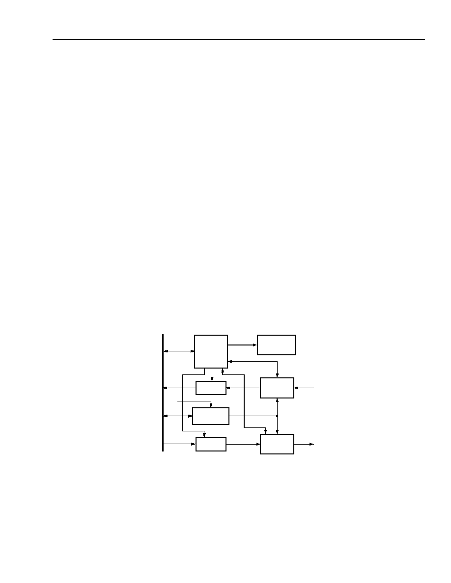
Agere Systems Inc.
187
Data Sheet
T8302 Internet Protocol Telephone
July 2001
Advanced RISC Machine (ARM )
14 IrDA_ACC and UART_ACC
There are two asynchronous communications controllers on the IPT_ARM. The IrDA_ACC provides an IrDA infra-
red channel and the UART_ACC provides a connection to the expansion UART unit. A list of features of the two
ACC follows:
s
Full-duplex asynchronous communication.
s
Each ACC has 10 x 32 FIFOs for both receive and transmit.
s
One start bit, eight data bits, one optional ninth data bit, one optional parity bit, one stop bit.
s
Separate programmable baud rates.
s
Complete status reporting capabilities.
s
Support for DMA transfers.
s
IrDA input/output pulse formatter option (IrDA_ACC only).
s
Programmable IrDA output pulse to meet infrared transmitter and receiver timing requirements. (IrDA_ACC only.)
14.1 ACC Operation
As shown in Figure 22 below, the function of the ACC is to convert incoming serial data on the receive line
(IrDA_RX, the RX inputs for IrDA_ACC, UART_ACC, respectively) to parallel data for the ARM, and convert parallel
data from the ARM to serial data on the transmit line (IrDA_TX, the TX outputs for IrDA_ACC, UART_ACC, respec-
tively). For each ACC the baud rate used to transmit and receive serial data is separately programmable using the
baud rate register
(see Table 170 on page 190)
and the sample mode field of the mode control register
(see
Table 176 on page 193)
. The status of the transmitter and receiver FIFOs are used to generate interrupts.
The transmit and receive FIFOs are 10 bits wide by 32 entries deep. In 8-bit mode, data is stored in bit 7 through bit
0 (LSB). For 8-bit transfers, bits 9 (MSB) and 8 are always ignored on reads and written to 0. For 9-bit transfers,
bit 9 is used to control the extended character support.
5-8221 (F)
Figure 22. ACC Block Diagram
PER
I
P
H
E
R
A
L
BU
S
CONTROL
Rx FIFO
BAUD RATE
GENERATOR
Tx FIFO
IRQ
INTERRUPT
CONTROLLER
Rx SHIFT
REGISTER
Tx SHIFT
REGISTER
Rx
Tx
CLK

188
Agere Systems Inc.
T8302 Internet Protocol Telephone
Data Sheet
Advanced RISC Machine (ARM )
July 2001
14 IrDA_ACC and UART_ACC
(continued)
14.1.1 Transmit and Receive Operation
In order to transmit data on the transmit line Tx, the baud rate register
(see Table 170 on page 190)
is set, the
sample mode field of the mode control register
(see Table 176 on page 193)
is set, the transmitter control reg-
ister is set
(see Table 175 on page 193)
, and then data is written into the transmitter FIFO. The data from the trans-
mitter FIFO is transferred to the transmitter shift register. A start bit is generated and then the data is shifted to
the output one bit at a time at the rate programmed in the baud rate register and the sample mode field of the
mode control register. The data transmitted is synchronized to the baud rate generator so the width of the start bit
does not vary. The optional parity bit is then generated, followed by stop bit(s).
To receive serial data from the Rx input pin, set the baud rate and the receiver control register
(see Table 173 on
page 192)
. When a start bit is detected, the data on the Rx line is shifted into the receiver shift register. This is
done by delaying one-half bit time and then sampling each data bit in the center of its ideal bit time. There is some
error when data is sampled if the baud rate counter does not match the baud rate exactly. The error introduced is
determined by the values programmed in the baud rate register and the sample mode field of the mode control
register. After shifting one character and the optional parity bit into the receiver shift register, the data is tested
for a parity error and the data is transferred to the receiver FIFO. If the controller detects receive errors, it sets
appropriate error bits in the FIFO status register
(see Table 172 on page 191)
and generates an interrupt if the
ACC interrupt enable register
(see Table 180 on page 196)
was set to enable the corresponding interrupt.
A single interrupt line for each ACC is connected to the interrupt controller. When the ARM receives an interrupt
from one of the ACCs, the interrupt type is read from the respective ACC's
interrupt
register.
14.1.2 Transfer Operating Modes
The ACC operates in several modes. There are 8 or 9 bits of data followed by optional parity bits. The receiver and
transmitter
can
operate in different parity modes but use the same number of data bits.
Table 167. ACC Transfer Modes
14.1.3 Programming the Baud Rate
The baud rate is programmed by setting values in two registers. Each bit period is divided into between 16 and
31 samples. This number is determined by adding 16 to the value set in SM of the mode control register
(see
Table 176 on page 193)
. The sample period is determined by multiplying the input clock period by the value in the
baud rate register + 1. These two values, when multiplied together, are as close as possible to the ideal number of
clocks per bit for the desired baud rate.
The input clock for the ACCs on the IPT_ARM is the system clock. The maximum and default baud rate for the ACC
(IrDA and UART) transmit and receive data is 115.2 kHz. The input clock is divided by 500 to achieve this exact
baud rate. The number of sample clocks could be selected as 25, programmed as 9 (see bits 7:4
of the mode con-
trol register
in
Table 176 on page 193
), and the baud rate register could be selected as 19, to set the clock divider
to 20.
Mode: Bit 0 of Mode
Control Register
Parity Control: Bits[4:3] of
Transmitter/Receiver Control Register
Resulting Transfer
0
00
1 start, 8 data, 1 stop bit.
0
01
1 start, 8 data, 2 stop bits.
0
10
1 start, 8 data, 1 even parity, 1 stop bit.
0
11
1 start, 8 data, 1 odd parity, 1 stop bit.
1
00
1 start, 9 data, 1 stop bit.
1
01
1 start, 9 data, 2 stop bits.
1
10
1 start, 9 data, 1 even parity, 1 stop bit.
1
11
1 start,
9
data, 1 odd parity, 1 stop bit.

Agere Systems Inc.
189
Data Sheet
T8302 Internet Protocol Telephone
July 2001
Advanced RISC Machine (ARM )
14 IrDA_ACC and UART_ACC
(continued)
For example:
Where BRD is programmed as 0x13 and SM is programmed as 0x9.
There is also an additional choice that reduces the error even more in some cases. If AL/CO of the mode control
register is set to 1, alternate mode is entered. In this mode, the least significant bit of the sample count is toggled
for every other bit. In alternate mode, for example, if the sample count is set to 23, then the first bit uses a sample
count of 23, the next bit 22, then 23, and so on. Using this mode reduces the error for some baud rate choices.
14.1.4 Extended Characters
The ACC can generate the following two types of special characters in 9-bit mode:
s
A break character.
s
An idle character.
A break character consists of 11 start bits (zeros) and an idle character consists of 11 stop bits (ones). To use
these extended characters, ECE of the mode control register is set to 1. To transmit these characters, write a
data value to the transmit FIFO according to Table 168. Idle characters have no effect on the receiver.
Table 168. Extended Characters
14.2 ACC Registers
Table 169. IrDA_ACC and UART_ACC Communication Controller Register Map
Data Value Range
Resulting Character
0x000:0x1FF
Normal 9-bit character.
0x200
Break character.
0x20:0x3FE
Do not write these values.
0x3FF
Idle character.
Register
IrDA_ACC Address
UART_ACC Address
Baud rate register
(see Table 170 on page 190)
.
0xE000 8000
0xE000 9000
Baud rate counter register
(see Table 171 on page 190)
.
0xE000 8004
0xE000 9004
FIFO status register
(see Table 172 on page 191)
.
0xE000 8008
0xE000 9008
Receiver control register
(see Table 173 on page 192)
.
0xE000 8010
0xE000 9010
Transmitter control register
(see Table 175 on page 193)
.
0xE000 8014
0xE000 9014
Mode control register
(see Table 176 on page 193)
.
0xE000 8018
0xE000 9018
Tx/Rx FIFO register
(see Table 177 on page 194)
.
0xE000 801C
0xE000 901C
IrDA feature register
(see Table 178 on page 194)
.
0xE000 8020
NA
ACC interrupt register
(see Table 179 on page 195)
.
0xE000 8040
0xE000 9040
ACC interrupt enable register
(see Table 180 on page 196)
.
0xE000 8044
0xE000 9044
aud rate =
system clock
BRD + 1
)
SM
16
)
+
(
(
---------------------------------------------------------
5.2 KHz =
57.6 MHz
19
1
+
(
)
)
9
16
)
+
(
(
-------------------------------------------------

190
Agere Systems Inc.
T8302 Internet Protocol Telephone
Data Sheet
Advanced RISC Machine (ARM )
July 2001
14 IrDA_ACC and UART_ACC
(continued)
14.2.1 Baud Rate Register
The baud rate register is used to divide the ACC clock to generate different baud rates. This divider is 16 bits
wide, hence division factors of 1--65,536 are programmable. The actual divider count used is the value in the baud
rate register + 1. The format of the baud rate register is shown below.
Table 170. Baud Rate Register
14.2.2 Baud Rate Counter Register
The baud rate counter register is a read-only register that returns the current value of the baud rate counter. This
counter is initialized with the value in the baud rate register after the counter counts down to 0, or if the baud rate
counter register is written.
Table 171. Baud Rate Counter Register
Address--IrDA 0xE000 8000, UART 0xE000 9000
Bit #
31:16
15:0
Name
RSVD
BRD
Bit #
Name
Description
31:16
RSVD
Reserved.
15:0
BRD
Baud rate divisor. Specifies the baud rate divisor. For a value of 0x0000, the resulting baud
rate divisor is 1. For a value of 0xFFFF, the resulting baud rate divisor is 65,536.
Address--IrDA 0xE000 8004, UART 0xE000 9004
Bit #
31:16
15:0
Name
RSVD
BRC
Bit #
Name
Description
31:16
RSVD
Reserved.
15:0
BRC
Baud rate counter. Current value of the baud rate counter.

Agere Systems Inc.
191
Data Sheet
T8302 Internet Protocol Telephone
July 2001
Advanced RISC Machine (ARM )
14 IrDA_ACC and UART_ACC
(continued)
14.2.3 FIFO Status Register
The FIFO status register informs the core of the status of the transmitter, receiver, and FIFOs. The FIFO status
register is a read-only register. Writes to its address are ignored. Table 172 shows the format of the FIFO status
register.
Table 172. FIFO Status Register
Address--IrDA 0xE000 8008, UART 0xE000 9008
Bit #
31:8
7
6
5
4
3
2
1
0
Name
RSVD
RID
TSE
TFF
TFHF
TFE
RFF
RFHF
RFE
Bit #
Name
Description
31:8
RSVD
Reserved.
7
RID
Receiver idle.
If 1, the receiver is idle.
If 0, the receiver is not idle.
6
TSE
TSR empty.
If 1, the transmitter shift register is empty.
If 0, the transmitter shift register is not empty.
5
TFF
Transmitter FIFO full.
If 1, the transmitter FIFO is full.
If 0, the transmitter FIFO is not full.
4
TFHF
Transmitter FIFO half full.
If 1, the transmitter FIFO is at least half full.
If 0, the transmitter FIFO is not at least half full.
3
TFE
Transmitter FIFO empty.
If 1, the transmitter FIFO is empty.
If 0, the transmitter FIFO is not empty.
2
RFF
Receiver FIFO full.
If 1, the receiver FIFO is full.
If 0, the receiver FIFO is not full.
1
RFHF
Receiver FIFO half full.
If 1, the receiver FIFO is at least half full.
If 0, the receiver FIFO is not at least half full.
0
RFE
Receiver FIFO empty.
If 1, the receiver FIFO is empty.
If 0, the receiver FIFO is not empty.

192
Agere Systems Inc.
T8302 Internet Protocol Telephone
Data Sheet
Advanced RISC Machine (ARM )
July 2001
14 IrDA_ACC and UART_ACC
(continued)
14.2.4 Receiver Control Register
The receiver control register controls the receiver FIFO, interrupts, and parity generation. On any reset, the
receiver control register is set to all zeros.
Table 173. Receiver Control Register
14.2.5 ACC Parity Bit Encoding
Table 174. ACC Parity Bit Encoding
14.2.6 Transmitter Control Register
The transmitter control register controls the transmitter FIFO, interrupts, and parity generation. On any reset, the
transmitter control register is set to all zeros. Table 175 shows the transmitter control register.
Address--IrDA 0xE000 8010, UART 0xE000 9010
Bit #
31:8
7
6:5
4:3
2:1
0
Name
RSVD
RD
RSVD
PC
RSVD
FR
Bit # Name
Description
31:8
RSVD Reserved.
7
RD
Receiver disable. Disables the receiver. Writing a 1 to this bit will disable the receiver.
6:5
RSVD Reserved.
4:3
PC
Parity check. Controls receiver parity checking. Table 174 below shows the encoding for this field.
Parity checking is disabled upon any reset.
2:1
RSVD Reserved.
0
FR
FIFO reset. Resets the receiver FIFO.
Writing 1 (constantly) to this bit resets the receiver FIFO, discarding data still there and marking it
empty.
Writing 0 to this bit causes the FIFO to accept new data.
The receiver FIFO is reset upon a reset to the IrDA_ACC.
Bits 4:3
Parity
00
No parity.
01
Mark parity (always send a 1).
10
Even parity.
11
Odd parity.

Agere Systems Inc.
193
Data Sheet
T8302 Internet Protocol Telephone
July 2001
Advanced RISC Machine (ARM )
14 IrDA_ACC and UART_ACC
(continued)
Table 175. Transmitter Control Register
14.2.7 Mode Control Register
The mode control register selects ACC mode options. On any reset, the mode control register is set to all
zeros. The mode control register is shown below.
Table 176. Mode Control Register
Address--IrDA 0xE000 8014, UART 0xE000 9014
Bit #
31:6
5
4:3
2
1
0
Name
RSVD
TOD
PC
RSVD
TXON
FR
Bit #
Name
Description
31:6
RSVD
Reserved.
5
TOD
Transmitter open drain. Puts the transmit output into open-drain mode.
If 1, open-drain.
If 0, normal.
4:3
PC
Parity control. Controls transmitter parity generation.
Table 174 on page 192
shows the
encoding for this field. Parity generation is disabled upon any reset.
2
RSVD
Reserved.
1
TXON
Transmitter on. A 1 must be written to this bit before the transmitter loads data from the
FIFO into the transmitter shift register and begins transmitting. This bit also serves as a
single location where the interrupts from the transmitter empty FIFO or its shift register
empty status bit can be disabled and masked when the transmitter is not in use.
0
FR
FIFO reset. Resets the transmitter FIFO.
If 1, the transmitter FIFO is reset, discarding remaining data and marking it as empty.
If 0, the FIFO can accept new data.
The transmitter FIFO is reset upon resetting the ACC.
Address--IrDA 0xE000 8018, UART 0xE000 9018
Bit #
31:8
7:4
3
2
1
0
Name
RSVD
SM
AL/CO
ECE
RSVD
9BM
Bit #
Name
Description
31:8
RSVD
Reserved.
7:4
SM
Sample mode. Selects the input sample clock that is equal to the decimal equivalent of
bits 7:4 plus 16.
3
AL/CO
Alternate/constant. Controls the special alternate mode.
If 1, the least significant bit of the sample count is toggled for each new bit of a transfer.
If 0, the sample count remains constant for each bit.
2
ECE
Extended character enable. Enables the extended characters in 9-bit mode.
If 1, the extended characters are available.
If 0, the extended characters are not available.
1
RSVD
Reserved.
0
9BM
9-bit mode. Indicates if the transfers are 8 or 9 bits.
If 1, all transfers consist of 9 data bits.
If 0, all transfers consist of 8 data bits.

194
Agere Systems Inc.
T8302 Internet Protocol Telephone
Data Sheet
Advanced RISC Machine (ARM )
July 2001
14 IrDA_ACC and UART_ACC
(continued)
14.2.8 Tx/Rx FIFO Register
The Tx/Rx FIFO register provides access to the transmitter and receiver FIFOs. A write to this register writes a
character to the transmitter FIFO. A read from this register reads a character from the receiver FIFO. Both FIFOs
are reset upon all system resets.
The ACC loads the output shift register
(see Figure 22 on page 187)
with data from the FIFO prior to transmitting
that character and stores the received character in the FIFO after it has been completely received, including its
stop character.
A read from an empty Rx FIFO returns the byte from the FIFO position just after the last Rx FIFO read, but it does
not change the status of the Rx FIFO.
Table 177. Tx/Rx FIFO Register
14.2.9 IrDA Feature Register
The IrDA feature register is used to control the IrDA and the device MUX. The IrDA feature register is set to all
zeros on any reset.
Table 178. IrDA Feature Register
Address--IrDA 0xE000 801C, UART 0xE000 901C
Bit #
31:10
9
8
7:0
Name
RSVD
EXFI
DB9
CHA
Bit #
Name
Description
31:10
RSVD
Reserved.
9
EXFI
Extended FIFO character mode. In 9-bit data mode, the value of bit 9 in the transmit FIFO
selects between the normal character mode (i.e., 1 start, 9 data bits, 1 optional parity, 1 stop),
and the break/idle mode (i.e., synchronous transmission of a break or idle line conditions for
11 baud intervals). In 8-bit data mode, this bit is ignored on writes and always read as zeros.
If 1, the character is an extended character.
If 0, the character is a normal character.
8
DB9
Data bit 9 mode. Bit 8 is the ninth data bit in 9-bit data mode. In 8-bit data mode, it is ignored
on writes and always reads as zeros.
7:0
CHA
Character. Character to transmit if written to. Character received if read from.
Address 0xE000 8020
Bit #
31:10
9
8
7:0
Name
RSVD
SEL
IDE
PWC
Bit #
Name
Description
31:10
RSVD Reserved.
9
SEL
Select. Must be 0.
8
IDE
IrDA enable. Enables the IrDA.
If 1, the IrDA is active and the IrDATx and IrDARx pins are driven by the IrDA feature.
If 0, the IrDA is disabled and the IrDATx and IrDARx pins are driven without the IrDA I/O formatter.
7:0
PWC
Pulse width count. Pulse width count value.

Agere Systems Inc.
195
Data Sheet
T8302 Internet Protocol Telephone
July 2001
Advanced RISC Machine (ARM )
14 IrDA_ACC and UART_ACC
(continued)
Table 179. ACC Interrupt Register
Address 0xE000 8040, 0xE000 9040
Bit #
31:12
11
10
9
8
7
6
Name
RSVD
TXNDI
TXSREI
TXFHI
TXFEI
RSVD
RXFNEI
Bit #
5
4
3
2
1
0
--
Name
RXNII
RXPEI
RXFEI
RXOEI
RXFHI
RXFFI
--
Bit #
Name
Description
31:12
RSVD
Reserved.
11
TXNDI
Transmitter no data interrupt. This bit is a 1 when the transmitter shift register is empty and
the transmitter FIFO is empty and the TXON bit is set to 1. If the TXNDIE is set when this bit is
1, an interrupt will be generated.
This bit is read-only.
10
TXSREI Transmitter shift register empty interrupt. This bit is set when the transmitter shift register
becomes empty. If the interrupt is enabled in the interrupt enable register and the TXON bit is
set to 1, an interrupt will be generated. A new byte of data must be loaded into the transmit
shift register to re-enable this bit to transition to 1 again.
9
TXFHI
Transmitter FIFO half-empty interrupt. This bit is a 1 when the transmit FIFO is less than half
full. The FIFO condition, that causes the interrupt to occur must be removed, (i.e., by writing the
FIFO) to remove this bit. This bit is read-only. This interrupt must be disabled if the processor
does not have any more data to place in the transmitter to prevent an interrupt from always
being asserted.
This bit is masked and will be a 0 if the TXON bit is not set to a 1.
8
TXFEI
Transmitter FIFO empty interrupt. This bit is a 1 when the transmit FIFO is empty. The FIFO
condition that caused the interrupt must be removed (i.e., by writing the FIFO) to remove this
bit. This bit is read-only. This interrupt must be disabled if the processor does not have any
more data to place in the transmitter to prevent an interrupt from always being asserted.
This bit is masked and will be a 0 if the TXON bit is not set to a 1.
7
RSVD
Reserved.
6
RXFNEI Receiver FIFO not empty interrupt. This bit is a 1 when the receive FIFO is not empty. The FIFO
condition that caused the interrupt must be removed (i.e., by reading the FIFO) to remove
this bit.
This bit is read-only.
5
RXNII
Receiver not idle interrupt. This interrupt is set when the receiver becomes not idle. If the
receiver not idle interrupt is enabled while this bit is 1, an interrupt to the processor will be gen-
erated. This bit is cleared by writing a 1 to this bit location. If the receiver is still not idle when
this bit is cleared, it must go idle and then not idle again for a new interrupt to be generated.
Note: RXNII does not indicate that an entire character has been received. It indicates that a
character receipt is in progress. To verify that an entire character has been received, poll
the RFE bit in the FIFO status register
(see Table 172 on page 191)
.
4
RXPEI
Receive data parity error. This bit is set when a parity error is detected in the received data. If
the parity error interrupt enable bit is set while this bit is 1, an interrupt will be generated.
This bit is cleared by writing a 1 to this bit location.
3
RXFEI
Receive data framing error. This bit is set when a framing error is detected in the received data.
If the framing error enable bit is set while this bit is 1, an interrupt will be generated.
This bit is cleared by writing a 1 to this bit location.

196
Agere Systems Inc.
T8302 Internet Protocol Telephone
Data Sheet
Advanced RISC Machine (ARM )
July 2001
14 IrDA_ACC and UART_ACC
(continued)
Table 179. ACC Interrupt Register (continued)
Table 180. ACC Interrupt Enable Register
Bit #
Name
Description
2
RXOEI
Receive data overrun error. This bit is set when a receive overrun error occurs. If the overrun
interrupt enable bit is set while this bit is 1, an interrupt will be generated.
This bit is cleared by writing a 1 to this bit location.
1
RXFHI
Receiver FIFO half-full interrupt. This bit is a 1 if the receiver FIFO is half full or more than half
full. The receiver FIFO must be read or reset to remove this condition.
This bit is read-only.
0
RXFFI
Receiver FIFO full interrupt. This bit is a 1 if the receiver FIFO is full. The FIFO condition that
caused this interrupt must be removed (i.e., by writing the FIFO to remove this bit).
This bit is read-only.
Address 0xE000 8044, 0xE000 9044
Bit #
31:12
11
10
9
8
7
6
Name
RSVD
TXNDIE
TXSREE
TXFHE
TXFEI
RSVD
RXFNFEI
Bit #
5
4
3
2
1
0
--
Name
RXNIE
RXPEI
RXFEI
RXOEI
RXFHI
RXFFI
--
Bit #
Name
Description
31:12
RSVD
Reserved.
11
TXNDIE
Transmitter no data interrupt enable.
If 1, the transmitter no data interrupt is enabled.
If 0, no transmitter no data interrupt will be generated.
10
TXSREE Transmitter shift register empty interrupt enable.
If 1, the transmitter shift register empty interrupt is enabled.
If 0, no transmitter shift register empty interrupt will be generated.
9
TXFHE
Transmitter FIFO half-empty interrupt enable.
If 1, the transmitter FIFO half-empty interrupt is enabled.
If 0, no transmitter FIFO half-empty interrupt will be generated.
8
TXFEI
Transmitter FIFO empty interrupt enable.
If 1, the transmitter FIFO empty interrupt is enabled.
If 0, no transmitter FIFO empty interrupt will be generated.
7
RSVD
Reserved.
6
RXFNFEI RXFNFEI receiver FIFO not empty interrupt enable.
If 1, the receiver FIFO not empty interrupt is enabled.
If 0, the receiver FIFO not empty interrupt is disabled.
5
RXNIE
Receiver not idle interrupt.
If 1, the receiver not idle interrupt is enabled.
If 0, no receiver not idle interrupt will be generated.
4
RXPEI
Received data parity error interrupt enable.
If 1, the received data parity error interrupt is enabled.
If 0, no received data parity error interrupt will be generated.

Agere Systems Inc.
197
Data Sheet
T8302 Internet Protocol Telephone
July 2001
Advanced RISC Machine (ARM )
14 IrDA_ACC and UART_ACC
(continued)
Table 180. ACC Interrupt Enable Register (continued)
14.3 IrDA Formatter
The IrDA formatter is only supported in the IrDA_ACC. The UART_ACC does not have this feature. It works with
the ACC to provide compatibility with the IrDA infrared serial data link standard. Features for the IrDA formatter fol-
low:
s
Operates at speeds of up to 115.2 kbits/s.
s
Programmable pulse width to the IrDA transceiver.
14.3.1 IrDA Formatter Operation
The IrDA formatter is enabled before it is used by setting IDE of the IrDA feature register
(see Table 178 on page
194)
.
Figure 23
shows how the output of the IrDA formatter follows the output of the IrDA_ACC channel. When the
IrDA_ACC output is 0, the IrDA outputs a pulse high. When the IrDA_ACC output is 1, there is no pulse during that
bit time. The width of the pulse is determined by the value programmed into the IrDA feature register using the fol-
lowing formula:
IrDA Pulse-Width = 8 x [Clock Period x (PWC + 1)]
The IrDA feature register
(see Table 178 on page 194)
is set to ensure that the pulse-width meets the minimum
required by the transceiver being used.
Bit #
Name
Description
3
RXFEI
Received data framing error interrupt enable.
If 1, the received data framing error interrupt is enabled.
If 0, no received framing error interrupt will be generated.
2
RXOE
Received data overrun error interrupt enable.
If 1, the received data overrun error interrupt is enabled.
If 0, no received overrun error interrupt will be generated.
1
RXFHI
Receiver FIFO half-full interrupt enable.
If 1, the receiver FIFO half-full interrupt is enabled.
If 0, no Receiver FIFO half-full interrupt will be generated.
0
RXFFI
Receiver FIFO full interrupt enable.
If 1, the receiver FIFO full interrupt is enabled.
If 0, no receiver FIFO full interrupt will be generated.

198
Agere Systems Inc.
T8302 Internet Protocol Telephone
Data Sheet
Advanced RISC Machine (ARM )
July 2001
14 IrDA_ACC and UART_ACC
(continued)
Figure 23. IrDA Transmit Data Timing Diagram and Width Programmability
Figure 24
shows how the IrDA formatting feature converts the IrDA pulse back into data compatible with ACC.
When the IrDA formatter receives a pulse low, the data is converted to a low for the ACC receive line. When a pulse
low is not seen, the data is held high. A pulse must be held for a minimum of two clock cycles of the baud rate
counter clock output for it to be detected by the IrDA formatter.
Reference
Parameter
Minimum
Maximum
t1
System Clock Cycle Time.
17.36 ns*
--
t2
IRDATAX0 Output Data Valid.
--
12.85 ns
t3
IRDATAX0 Output Hold Time.
0 ns
--
* Nominal clock period.
INTERNAL
ASYNC DATA
SYSTEM
CLOCK
57.6 MHz
IRDATAX0
CLOCK
EDGE 1
Bit 0
Bit 1
t3
t2
t1
COUNT = 2088 CLOCKS/20 kHz BAUD
PROGRAMMABLE PULSE WIDTH (PWC)
PROGRAMMABLE BIT TIME/BAUD RATE
CLOCK

Agere Systems Inc.
199
Data Sheet
T8302 Internet Protocol Telephone
July 2001
Advanced RISC Machine (ARM )
14 IrDA_ACC and UART_ACC
(continued)
Figure 24. IrDA Receive Data Timing Diagram, Minimum Pulse Width
14.4 DMA Support for ACC I/O Data
The DMA controller transfers data to and from the Tx/Rx FIFO registers. By selecting the proper mode and
device, the ACCs are accessed.
When the ACC is in 8 bit mode, the lower 8 bits of the DMA transfer are valid. In
9-bit data bit mode, the lower 9 bits of the DMA transfer are valid.
14.5 Operation on Reset
Upon any reset, the ACC performs the following:
s
All ongoing transfers are aborted.
s
Both transmitter and receiver FIFOs are reset.
s
The transmitter control register is reset to all zeros to disable transmitter parity generation.
s
The receiver control register is reset to all zeros to disable receiver parity checking.
s
The FIFO status register is set to reflect the current status of both transmitter and receiver FIFOs (empty).
s
The baud rate register is reset to all zeros.
Reference
Parameter
Minimum
Maximum
t1
System Clock Cycle Time.
17.36 ns*
--
t2
IRDARX0 Setup Time.
2.25 ns
--
t3
IRDARX0 Hold Time (2 Clocks + Hold).
37.7 ns
--
* Nominal clock period.
IRDARX0
t1
Bit 0
Bit 1
t2
t3
HIGH SAMPLES
TWO CLOCK MINIMUM IrDA PULSE
PROGRAMMABLE BAUD RATE

200
Agere Systems Inc.
T8302 Internet Protocol Telephone
Data Sheet
Advanced RISC Machine (ARM )
July 2001
15 Synchronous Serial Interface (SSI)
The SSI unit is compatible with the SPI interface of the Motorola
*
68HC11 microcontroller. The following features of
the SPI interface are supported by the SSI interface:
s
Four-wire synchronous serial interface clock, data in, data out, slave select control.
s
Clock polarity selection.
s
Data phase selection.
s
Outputs can be programmed to be open-drain or direct-drive.
s
Four-wire full-duplex transfers.
s
Three-wire half-duplex or unidirectional transfers.
s
Detection of multiple-master bus contention faults and slave-mode write-collisions.
s
Support for DMA transfers.
15.1 Description
The SSI unit operates in either the master mode or the slave mode.
Figure 25 on page 202
shows a functional
block diagram of the SSI. The master unit in an SSI cluster enables slave units to receive and transmit data, and ini-
tiates transmissions by broadcasting a clock signal, called SCK, to all other units. A data register in each unit oper-
ates as an 8-bit shift register clocked by SCK. The master unit configures a data path between its data register and
the data register of one other slave unit, so that a 16-bit circular shift register is formed. Communication between
the master and slave units then occurs if eight SCK cycles cause the data values, stored in each register, to be
exchanged. This mode of operation is suitable for bidirectional communication between a master and slave unit. It
utilizes the four-wire interface consisting of clock, data in, data out, and slave select control.
Other possible modes of operation are as follows.
s
A master unit broadcasts a byte (or longer multibyte message) to several slave units simultaneously, provided
that only one slave is enabled to drive data back to the master.
s
A multimaster, multislave network may be constructed where a software protocol allows all units to share the two
data transmit/receive wires without data loss.
s
Slave units are capable of receiving data and returning data when only one data wire is connected in the system.
Pins MDISDO and MDOSDI are tied together to form a single bidirectional data line. The MDISDO, MDOSDI,
and SCK pins are configured as open-drain outputs to minimize contention from several drivers that is possible in
some of these configurations. An external pull-up resistor is required on all open-drain pins.
15.1.1 Clocks
SCK is provided by the master unit and in the SSI. Seven different SCK rates derived from the system clock are
supported. If configured as a slave unit, SCK is obtained from outside of the device, and is assumed to be asyn-
chronous with respect to the slave's system clock. Consequently, data transfers and error conditions also occur
asynchronously with respect to the slave's system clock. A special register access sequence is defined for the
ARM core to obtain data and status information from the slave SSI. Depending on the polarity of the shift clock and
the phase of the data relative to the shift clock, the SSI interface supports four different modes of transfer. These
modes are under program control, and master and slave units communicate in a common mode.
* Motorola is a registered trademark of Motorola Inc.

Agere Systems Inc.
201
Data Sheet
T8302 Internet Protocol Telephone
July 2001
Advanced RISC Machine (ARM )
15 Synchronous Serial Interface (SSI)
(continued)
The 8-bit data register shifts out a byte, one bit at a time (MSB first), synchronously with the shift clock SCK. If run-
ning as a master, the SSI derives SCK from its system clock using a prescaling value determined by the
SCLK[2:0] bits of SSI control register 1
(see Table 183 on page 204)
. Before being output to the pin, the pre-
scaled clock is conditioned in the clock control block in accordance with the SPOL and SPHA bits in SSI control
register 1. As a slave, the shift clock is supplied by an external master through the SCK pin and is modified in
accordance with the SPOL and SPHA bits in the slave's SSI control register 1.
15.1.2 Date Transfer
The data register loads data from the lower byte of the peripheral bus. The received data is double buffered and is
read on the lower byte of the peripheral bus.
The status and shift control logic directs the transfer of data and generates status flags for end-of-transfer
(SDONE) and detectable error conditions (WCOLL and MODF). The bits from the SSI control registers are used
by the clock divide, clock control, status/shift/control, and the I/O control logic for proper operation.
The I/O control logic routes the data to and from the I/O pins as shown below.
15.1.3 Pin Configuration
Because a master MDISDO is the data input, MDOSDI is the data output and SCK is the serial clock output. SSN
is the slave select signal and is always an input to the SSI unit, whether the unit is a master or a slave. If a master,
the SSN input pin detects bus contention with another master in a multimaster system.
Because a slave MDISDO is the data output, MDOSDI is the data input, SCK is the serial clock input, and SSN is
the slave select input. The I/O control logic is directly controlled by the MSTR bit of SSI control register 1.
15.1.4 SSN Input
If SSN is low in a slave unit, the slave SSI is selected by the master for operation. If low in a master unit, this pin
indicates that there is contention with another master in the system, and this will be detected as a mode fault error
if SSNEN of SSI control register 1 is set to 1. The SSN pin is used by the SSI hardware (as long as SSNEN of
SSI control register 1 is one) but can also be read by master or slave software from SSN of SSI control
register 2. Bit 0 of SSI control register 2 reflects the state of the SSN pin, regardless of the state of SSNEN of
SSI control register 1.
15.1.5 Configurations
Multimaster: in a multiple-master system, all SCK pins are tied together, all MDOSDI pins are tied together, and all
MDISDO
pins are tied together.
Master--slave: a single SSI device is configured as a master and all other SSI devices on the SSI bus are config-
ured as slaves. The master drives data onto its SCK and MDOSDI pins to the SCK and MDOSDI pins of the
slaves.
The slave, whose SSN input pin is low, optionally drives data out onto its MDISDO pin to the MDISDO pin of the
master. The SCK, MDOSDI, and MDISDO pins are configured to behave as open-drain drivers using bits in SSI
control register 1. This prevents contention on these signals if more than one SSI device tries to simultaneously
drive the line. An external pull-up resistor is required on all open-drain pins.

202
Agere Systems Inc.
T8302 Internet Protocol Telephone
Data Sheet
Advanced RISC Machine (ARM )
July 2001
15 Synchronous Serial Interface (SSI)
(continued)
15.1.6 Slave Chip Select
There is one signal associated with SSI operation that is not part of the SSI unit. This is the slave chip select output
from the microcontroller. Software in the ARM processor uses one or more of the PPI general-purpose I/O pins as
output pins for the slave select signals it sends to the SSI slaves.
5-6667 (F)
Legend:
A--SSI control register 1, bits MSTR, SPHA.
B--SSI control register 1, bit MSTR.
C--SSI control register 1, bits SCLK [2:0].
D--SSI control register 1, bits EN, MSTR, SPOL, SPHA.
E--SSI control register 1, bits EN, MSTR, SPOL, SPHA, SDOEN, SSNEN.
F--SSI interrupt register, bits SDONE, WCOLL, MODF.
Figure 25. SSI Functional Block Diagram
PERIPERAL BUS
DATA REGISTER
MSB
LSB
DATA READ REGISTER
8-bit SHIFT REGISTER
SERIAL DATA OUT
SHIFT
CLOCK
˜
128
CLOCK
DIVIDE
˜
64
˜
32
˜
16
˜
8
˜
4
˜
2
CLOCK
CONTROL
CONTROL REGISTER
STATUS AND
SHIFT
CONTROL
IRQ14
PERIPHERAL BUS
SCK_OUT
SCK_IN
SSN
SSN
SCK
MDOSDI
MDISDO
M
S
S
M
S
S
SERIAL
DATA IN
TO/FROM
ARM CORE
CONTROL
2
A
B
C
D
E
F
M
I/O

Agere Systems Inc.
203
Data Sheet
T8302 Internet Protocol Telephone
July 2001
Advanced RISC Machine (ARM )
15 Synchronous Serial Interface (SSI)
(continued)
15.2 SSI Registers
The SSI unit has five programmable registers. The SSI data register is used for writing the 8-bit byte to be trans-
mitted and for reading the received 8-bit byte. SSI control registers 1 and 2 enable and configure the SSI for
serial communication in the desired mode. The SSI interrupt register and the SSI interrupt enable register dis-
play and enable interrupts, respectively. Table 181 below shows the register map of the SSI.
Table 181. SSI Register Map
15.2.1 SSI Data Register
The SSI data register contains the transmitted and received data bytes. The data byte that is transmitted is written
in the low-order byte of the SSI data register. The SSI data register is single buffered on the transmit side and
serves as the shift register for clocking out the bits with SCK.
The SSI data register is double buffered on the receive side. If all 8 bits are shifted in, the received data is copied
to a buffer register. The processor reads the contents of this register to determine the received word. Double buff-
ering on the receive side allows a new data byte to be shifted in while the previous one is read.
If in slave mode, the SSI uses the SCK pin to shift the SSI data register. While in master mode, it uses its internal
version of SCK.
For cases where SPHA = 1 and SSN is kept low between transfers, it is necessary to write bit SSNEN to 0
(in SSI control register 1) before writing the slave's SSI data register.
Table 182. SSI Data Register
On reset, all SSI data register bits are set to 0.
Register
Address
SSI data register
(see Table 182 on page 203)
.
0xE000 4000
SSI control register 1
(see Table 183 on page 204)
.
0xE000 4004
SSI control register 2
(see Table 185 on page 206)
.
0xE000 4008
SSI interrupt register
(see Table 186 on page 206)
.
0xE000 4010
SSI interrupt enable register
(see Table 187 on page 207)
.
0xE000 4014
Address 0xE000 4000
Bit #
31:8
7:0
Name
RSVD
TDWR
Bit #
Name
Description
31:8
RSVD
Reserved. Must be written with zeros.
7:0
TDWR
Transmit/receive data. Transmit data on write, receive data on read.

204
Agere Systems Inc.
T8302 Internet Protocol Telephone
Data Sheet
Advanced RISC Machine (ARM )
July 2001
15 Synchronous Serial Interface (SSI)
(continued)
15.2.2 SSI Control Register 1
SSI control register 1 is used to enable communication, set up the SSI in master/slave mode, report status, and
configure the clock.
Table 183. SSI Control Register 1
Address 0xE000 4004
Bit #
31:16
15
14
13
12
Name
RSVD
EN
MSTR
SPOL
SPHA
Bit #
11
10
9
8:3
2:0
Name
SDOEN
SSNEN
MDOEN
RSVD
SCLK
Bit #
Name
Description
31:16
RSVD
Reserved.
15
EN
Enable. Enables or disables the SSI.
If 1, the SSI is enabled.
If 0, it is disabled.
14
MSTR
Master mode. Configures the SSI in master or slave mode.
If 1, the SSI is configured in master mode.
If 0, it is configured in slave mode.
13
SPOL
Idle state. Determines the idle state of the SCK clock.
If 1, the SCK clock is idle at logic 1.
If 0, it is idle at logic 0.
12
SPHA
Data change. Determines when the data changes in each SCK cycle.
If 1, output data is shifted at the leading transition of SCK and input data is sampled at the mid-
point transition of SCK.
If 0, output data is shifted at the midpoint transition of SCK and input data is sampled at the
leading transition of SCK.
11
SDOEN
Output enable. Enables output from the MDISDO pin if the SSI is configured as a slave.
If 1, output from the MDISDO pin is enabled if the SSI is configured as a slave.
If 0, output is disabled.
A master SSI device simultaneously broadcasts a message to several slaves as long as no
more than one of the slaves tries to drive the MDISDO line. Also, SSI systems that tie MDOSDI
and MDISDO together to form a single bidirectional data line also need to selectively disable
the MDISDO output.
10
SSNEN
SSN enable.
If 1 in master mode, the SSN input is enabled and causes a mode fault.
If 0 in master mode, the SSN input is disabled.
If 1 in slave mode, the slave uses the SSN input to determine if it is selected for operation.
If 0 in slave mode, the slave is not selected for operation.
9
MDOEN MDOSDI enable. Enables output from the MDOSDI pin if the SSI is configured as master.
If 1, output from the MDOSDI pin is enabled if the SSI is configured as master.
If 0, output is disabled.
Bit 9 is 0 when the master SSI wants to receive a byte of data from a slave without transmitting
a byte.

Agere Systems Inc.
205
Data Sheet
T8302 Internet Protocol Telephone
July 2001
Advanced RISC Machine (ARM )
15 Synchronous Serial Interface (SSI)
(continued)
Table 183. SSI Control Register 1 (continued)
Table 184. SSI Clock Divide Bit Encoding
15.2.3 SSI Control Register 2 Bit Descriptions
SSI control register 2 configures the SSI in FASTCLEAR mode, reads the value of the SSN pin, and configures
several outputs as open-drain.
15.2.3.1 SSN
SSN reflects the value on the chip's SSN pin. Software in both the master and slave SSI units read this register, but
it is used only by the slave SSI software. By polling this register bit, the slave SSI software determines if the slave
has been selected for operation. The slave is selected for operation if bit 0 (SSN) of SSI control register 2 is 0.
However, note that monitoring the SSN pin is not a reliable indicator of a transfer in progress in the slave if
SPHA = 1 since (in that case) the SSN pin stays low between bytes transferred. If SPHA = 0, monitoring of the
SSN pin indicates whether a byte transfer is in progress since SSN is taken high between transfers.
Since the SSN pin is synchronized with the SSI system clock before being read and made available in the register
bit, the SSN pin must hold its level (0 or 1) a minimum of two system clocks to ensure that the level is recognized in
bit 0 of SSI control register 2.
15.2.3.2 FASTCLEAR
FASTCLEAR of SSI control register 2 is the FASTCLEAR bit. This bit clears to 0 after reset.
If this bit is set, the
SDONE and MODF bits of the SSI interrupt register are cleared upon a read/write of the SSI data register.
FASTCLEAR is set when performing DMA transfers from the SSI so that the SDONE and MODF bits do not have
to be written to be cleared.
Slave units are capable of receiving data and returning data when only one data wire is
connected in the system.
15.2.3.3 MDOD
Bit 3 of SSI control register 2 is the MDOSDI/MDISDO open-drain (MDOD) bit. This bit selects open-drain or
direct-drive output for MDOSDI and MDISDO when they are outputs. If bit 3 is 0, MDOSDI (master) or MDISDO
(slave) is direct-drive. If bit 3 is 1, MDOSDI (master) or MDISDO (slave) is open-drain.
Bit #
Name
Description
8:3
RSVD
Reserved. Must be set to 1.
2:0
SCLK
Clock configuration. Defines the clock prescale factor. For the encoding of bits 2:0 refer to
Table 184 below.
Bits [2:0]
Clock Divide
000
2
001
4
010
8
011
16
100
32
101
64
110
128
111
Reserved

206
Agere Systems Inc.
T8302 Internet Protocol Telephone
Data Sheet
Advanced RISC Machine (ARM )
July 2001
15 Synchronous Serial Interface (SSI)
(continued)
15.2.3.4 SCOD
Bit 4 of SSI control register 2 is the SCK open-drain (SCOD) bit. This bit selects open-drain or direct-drive output
from SCK when in master mode. If bit 4 is 0, SCK is direct-drive. If bit 4 is 1, SCK is open-drain.
Table 185. SSI Control Register 2
Note: On all resets, bit 0 of SSI control register 2 is set to 1 all other bits are set to 0.
Table 186. SSI Interrupt Register
Address 0xE000 4008
Bit #
31:5
4
3
2
1
0
Name
RSVD
SCOD
MDOD
RSVD
FASTCLEAR
SSN
Bit #
Name
Description
31:5
RSVD
Reserved.
4
SCOD
SCOD bit. This is the SCK open-drain (SCOD) bit. This bit selects open-drain or direct-
drive output for SCK.
If bit 4 is 0 when in master mode, SCK is direct-drive.
If bit 4 is 1, SCK is open-
drain
.
When an open-drain I/O buffer is used, the SCK output will be open-drain, regardless of
the state of bit 4.
3
MDOD
MDOSDI and MDISDO output. This bit selects open-drain or direct-drive output, for
MDOSDI and MDISDO when they are outputs.
If bit 3 is 0, MDOSDI (master) or MDISDO (slave) is direct-drive.
If bit 3 is 1, MDOSDI or MDISDO are open-drain.
When an open-drain I/O buffer is used, the MDISDO/MDOSDI output will be open-
drain, regardless of the state of bit 3.
2
RSVD
Reserved.
1
FASTCLEAR
Clear bit. This bit clears to 0 after reset. If this bit is set to 1, it is not necessary to
write
the MODF and SDONE bits of
the interrupt register
.
This bit is set for DMA operations with the SSI.
0
SSN
SSN state. SSN of SSI control register 2 always reflects the state of the SSN chip,
regardless of whether SSNEN is 0 or 1.
Address 0xE000 4010
Bit #
31:8
7
6
5
4
3:0
Name
RSVD
SDONE
WCOLL
MODF
RD_ORUN
RSVD
Bit #
Name
Description
31:8
RSVD
Reserved.
7
SDONE
Serial transfer complete interrupt.
If 1, the serial transfer is completed.
If 0, no transfer pending or a transfer is in progress.
Cleared by writing a 1.
6
WCOLL
Write collision error interrupt.
If 1, a write to the SSI data register occurred while a serial transfer was in progress.
If 0, no error was detected.
Cleared by writing a 1.

Agere Systems Inc.
207
Data Sheet
T8302 Internet Protocol Telephone
July 2001
Advanced RISC Machine (ARM )
15 Synchronous Serial Interface (SSI)
(continued)
Table 186. SSI Interrupt Register (continued)
Table 187. SSI Interrupt Enable Register
15.3 SSI Operation
The SPOL and SPHA bits in SSI control register 1 determine the mode of data transfer. Both of these bits control
the type of shift clock (SCK) generated. SPOL controls the polarity of SCK and SPHA determines the phase at
which the serial transfer begins. The latter leads to a fundamentally different type of transfer with implications in sit-
uations where back-to-back byte transfer is required. The transfer formats are different for different peripheral
devices but remain unchanged during a transfer between the master and the slave device. The SSI is flexible
enough to allow any desired configuration that conforms to the HC11 specifications. The different transfer formats
are now considered in detail.
Bit #
Name
Description
5
MODF
Mode fault error interrupt.
If 1, the SSN input was asserted while the unit was in master mode and SSNEN was enabled.
If 0, no error is detected.
Cleared by writing a 1.
4
RD_ORUN Read overrun error interrupt. This bit can only be set if the SSI is in master mode.
If 1, a byte received from the slave was written to the master's receive data buffer before the
previous byte from the slave had been read from that buffer.
3:0
RSVD
Reserved.
Address 0xE000 4014
Bit #
31:8
7
6
5
4
3:0
Name
RSVD
SDONEE
WCOLLE
MODFE
RD_ORUNE
RSVD
Bit #
Name
Description
31:8
RSVD
Reserved.
7
SDONEE
Serial transfer complete interrupt enable.
If 1, the serial transfer interrupt is enabled.
If 0, no serial transfer interrupt will occur.
6
WCOLLE
Write collision error interrupt enable.
If 1, the write collision interrupt is enabled.
If 0, no write collision interrupt will occur.
5
MODFE
Mode fault error interrupt enable.
If 1, the mode fault interrupt is enabled.
If 0, no mode fault interrupt will occur.
4
RD_ORUNE Read overrun error interrupt enable.
If 1, the read overrun interrupt is enabled.
If 0, no read overrun interrupt will occur.
3:0
RSVD
Reserved.

208
Agere Systems Inc.
T8302 Internet Protocol Telephone
Data Sheet
Advanced RISC Machine (ARM )
July 2001
15 Synchronous Serial Interface (SSI)
(continued)
15.3.1 SPHA = 0 Format
Figure 26 below shows the timing diagram of the serial byte transfer if SPHA = 0. SCK is shown for both cases of
SPOL, i.e., SPOL = 0 and SPOL = 1. The MDOSDI signal is the output of the master and the input to the slave. The
MDISDO signal is output from the slave and input to the master. The timing diagrams are interpreted either from
the master's or the slave's side. The SSN line is the slave select line. On the slave side, the transfer begins when
the SSN line is pulled low. For the master, transfer begins when data is written into its data register.
(Such a write is necessary even if the master is only interested in receiving data from the slave.)
Figure 26. SSI Transfer Timing Diagram, (SPHA = 0)
Reference
Parameter
Minimum
Maximum
t1
SCK Cycle Time.
--
--
t2
SCK Output Fall Time.
--
10%--90%
t4
SCK Output Rise Time.
--
10%--90%
t5
Slave Enable Lead Time.
0 ns
--
t6
Output Data Valid After Clock.
--
17.55 ns
t7
Slave Input Data Setup Time.
1.0 ns
--
t8
Input Data Hold Time.
1.0 ns
--
t9
Slave Data Out Access Time.
--
7.10 ns
t10
Output Data Hold Time After Clock.
0 ns
--
t11
Slave Disable Idle Time (Hold).
5 ns
--
SCK CYCLE
SCK
(SPOL = 0)
(SPOL = 1)
SCK
(FROM MASTER)
MDOSDI
(FROM SLAVE)
MDOSDO
(TO SLAVE)
SSN
MSB
6
5
4
3
2
1
0
(LSB)
MSB
6
5
4
3
2
1
0
(LSB)
t9
t10
t1
t4
t2
t5
t6
t8
t7
t11
(FOR REFERENCE)
MD
I
SDO
(FROM SLAVE

Agere Systems Inc.
209
Data Sheet
T8302 Internet Protocol Telephone
July 2001
Advanced RISC Machine (ARM )
15 Synchronous Serial Interface (SSI)
(continued)
15.3.1.1 Master Operation
In the master, the data is sampled from MDISDO at the rising edge of SCK and shifted onto MDOSDI at the falling
edge if SPOL = 0. If SPOL = 1, the sampling and shifting edges are reversed. At the end of eight cycles, the trans-
fer is completed for the master. On the eighth sampling SCK edge, the received byte is transferred to the read data
buffer, the SDONE status flag is set, and an interrupt, if enabled, is generated. The MDOSDI line stays high before
the transfer begins and after it ends. This is useful in multiple master systems where the MDOSDI line is always at
a known state whenever the control of the bus is relinquished to another master.
15.3.1.2 Slave Operation
On the slave side, data is sampled from MDOSDI at the rising edge of SCK and shifted onto MDISDO at the falling
edge if SPOL = 0. If SPOL = 1, the sampling and shifting edges are reversed. The received data is buffered on the
eighth sampling SCK edge, the SDONE flag is set, and the interrupt, if enabled, is generated. The end of transfer,
however, is indicated only if the SSN signal is deasserted. At that time, the MDISDO output pin stops driving.
Note: In multiple byte transfers, the SSN line is asserted and deasserted between successive bytes if SPHA = 0.
If the master sends another byte before deasserting and reasserting the SSN line, then the transfer is not guaran-
teed to be correct.
15.3.2 SPHA = 1 Format
Figure 27
shows the timing diagram of the serial byte transfer if SPHA = 1. SCK is shown for both cases of SPOL,
i.e., SPOL = 0 and SPOL = 1. The MDOSDI signal is the output of the master and input to the slave. The MDISDO
signal is the output from the slave and input to the master. The timing diagrams are interpreted either from the
master's or the slave's side. The SSN line is the slave select line.
The slave output is enabled as long as SSN is held low.
Note: In multiple byte transfers, the SSN line is held asserted (low) between successive bytes if SPHA = 1. The
SSN line can be tied low if SPHA = 1.

210
Agere Systems Inc.
T8302 Internet Protocol Telephone
Data Sheet
Advanced RISC Machine (ARM )
July 2001
15 Synchronous Serial Interface (SSI)
(continued)
Figure 27. SSI Transfer Timing Diagram, (SPHA = 1)
15.3.2.1 Master
The data in the master is sampled from MDISDO at the falling edge of SCK and shifted onto MDOSDI at the rising
edge if SPOL = 0. If SPOL = 1, the sampling and shifting edges are reversed. At the end of eight active levels of
SCK, the transfer is completed for the master. In effect, this occurs at the end of seven and a half cycles of the shift
clock. On the eighth sampling SCK edge, the received byte is transferred to the read data buffer, the SDONE status
Reference
Parameter
Minimum
Maximum
t1
SCK Cycle Time.
--
--
t2
SCK Output Fall Time.
--
10%--90%
t3
SCK Output Rise Time.
--
10%--90%
t4
Slave Enable Lead Time.
0 ns
--
t5
Output Data Valid After Clock.
--
17.55 ns
t6
Slave Input Data Setup Time.
1.0 ns
--
t7
Input Data Hold Time.
1.0 ns
--
t8
Slave Data Out Access Time.
--
7.1 ns
t9
Input Data Hold Time After Clock.
1.0 ns
--
t10
Slave Disable Idle Time.
5 ns
--
t11
Output Data Hold Time After Clock.
0 ns
--
SCK CYCLE
SCK
(SPOL = 0)
(SPOL = 1)
SCK
(FROM MASTER)
MDOSDI
(FROM SLAVE)
MDOSDO
(TO SLAVE)
SSN
MSB
6
5
4
3
2
1
0
(LSB)
MSB
6
5
4
3
2
1
0
(LSB)
t8
t9
t1
t3
t2
t4
t5
t6
t10
(FOR REFERENCE)
t11
t7
MD
I
SDO
(FROM SLAVE

Agere Systems Inc.
211
Data Sheet
T8302 Internet Protocol Telephone
July 2001
Advanced RISC Machine (ARM )
15 Synchronous Serial Interface (SSI)
(continued)
flag is set, and an interrupt, if enabled, is generated. The MDOSDI line stays high before the transfer begins and
after it ends. This is useful in multiple master systems where the MDOSDI line is always at a known state whenever
the control of the bus is relinquished to another master.
15.3.2.2 Slave
On the slave side, the data is sampled from MDOSDI at the falling edge of SCK and shifted onto MDISDO at the
rising edge if SPOL = 0. If SPOL = 1, the sampling and shifting edges are reversed. The received data is buffered
at the end of seven and a half shift clock cycles (i.e., on the eighth sampling SCK edge), the SDONE flag is set, the
interrupt, if enabled, is generated, and the end of transfer is indicated. The output, however, remains valid until
SSN is deasserted. At that time, the MDISDO pin stops driving.
15.3.3 Transfer Start
Every SSI transfer consists of an initiation period, followed by eight SCK cycles if the 8-bit data transfer takes
place, and finally the ending period. The details for the data transfer were considered in the previous section. Here
the initiation period is discussed for each of the different formats selected for the master and slave modes of oper-
ation.
If the SSI is configured as a master, all transfers are initiated by a write to the SSI data register. Such a write is
necessary even if the master is only interested in receiving data from the slave. There is a delay of three system
clock cycles after the write access before the start of the serial transfer. If SPHA = 0, SCK remains at its idle state
for the first half of the cycle following the write to the SSI data register. If SPHA = 1, the transfer cycle begins
immediately with the SCK going from its inactive level to the active level.
If the SSI is configured as a slave and SPHA = 0, a transfer begins if the SSN line is pulled low. The MSB of the
data written in the slave SSI data register initially appears on the MDISDO line. If the SSI is configured as a slave
and SPHA = 1, a transfer begins with the first active edge of SCK, provided that the slave is selected (SSN
asserted).
15.3.4 Transfer End
A transfer is complete if all 8 bits are shifted in serially, the data is transferred to the read data buffer, and the
SDONE flag is set. The interrupt signal (IRQ) will be active if SDONEE is set in the SSI interrupt enable register.
15.3.4.1 Master Operation
If the SSI is configured as a master, the received byte is transferred to the read-buffer at the end of eight SCK clock
cycles. The SDONE flag is set after a delay (independent of the SCK rate) of one system clock cycle.
15.3.4.2 Slave Operation
If the SSI is configured as a slave, the ending period depends on the value of SPHA. If SPHA = 0, SDONE is set at
the end of the eighth SCK cycle (one-half SCK cycle after the last bit is sampled by the slave). If SPHA = 1,
SDONE is set in the middle of the eighth SCK cycle (at the time the last bit is sampled). Since the master always
ends the transfer at the end of the eighth SCK cycle, the SDONE bit in the slave completes the transfer
if SPHA = 1.

212
Agere Systems Inc.
T8302 Internet Protocol Telephone
Data Sheet
Advanced RISC Machine (ARM )
July 2001
15 Synchronous Serial Interface (SSI)
(continued)
15.3.5 Interrupt Generation
If the SSI interrupt is enabled in the interrupt controller's SSI interrupt enable register, the SSI asserts its interrupt
request whenever a byte is successfully shifted in and copied to the read data buffer (i.e., if the SDONE bit is true,
or if a mode fault or read overrun occurs).
The interrupt is cleared if SDONE, MODF, and RD_ORUN are cleared.
15.3.6 Status Flags and Error Conditions
The SSI interrupt register contains four read-only status bits, SDONE, WCOLL, MODF, and RD_ORUN.
There is another error condition that occurs if the SSI is configured as a slave and a transfer is aborted by the mas-
ter unit pulling SSN high or the slave software writing SSI control register 1 bit 10:0 before the transfer is com-
plete. This error condition is not indicated by the status flags and is detected by a software protocol.
The status and error conditions are described below.
15.3.6.1 SDONE
SDONE is a status flag that indicates the end of a transfer. At the end of a transfer, the SDONE bit of SSI interrupt
register is set. If the FASTCLEAR bit of SSI control register 2 = 1, the SDONE flag is cleared by a read or write
of the SSI data register. If FASTCLEAR of SSI control register 2 = 0, the SDONE flag is cleared by writing to the
SDONE bit in the SSI interrupt register to clear the SSI interrupt.
15.3.6.2 WCOLL Flag
The WCOLL bit of SSI interrupt register indicates that a write collision error occurred. A write collision error is
detected if a write to the SSI data register is attempted while a transfer is in progress. The transfer continues but
the data that caused the error may or may not be written to the transmit buffer. Because of this uncertainty, a trans-
fer that experiences a write collision error is aborted and should be tried later. If the SSI is configured as a master,
a transfer begins when data is written to the SSI data register and ends when the received data is transferred to
the read data buffer, at which time SDONE is set.
Note: A write collision error should not occur in master mode if the driver software is structured correctly.
If the SSI is configured as a slave, it has no way to predict when the master will initiate a transfer. However, if
SPHA = 0, the true end of the transfer does not occur until the SSN signal is deasserted. In this case, the user
determines both the beginning and the end of transfer by polling the SSN line using bit 0 of SSI control register 2.
The SPHA = 1 mode is more problematic since SSN is held low constantly or between transfers so SSN cannot
always be used to tell whether a transfer is in progress. The end of transfer is determined via the SDONE flag in the
SSI interrupt register, but there is no satisfactory way of determining the beginning of transfer. Therefore, write
collisions are possible for this mode. However, these write collisions in the slave are avoided by writing
SSNEN
of
SSI control register 1 to zero before writing the slave's SSI data register. If SSNEN of SSI control register 1 is
written to 0 during a transfer, the transfer terminates.
The WCOLL flag, once set, is cleared by writing a 1 to the WCOLL field in the SSI interrupt register, followed by
a read or write of the SSI data register.
15.3.6.3 MODF
The MODF bit indicates a mode fault. A mode fault error occurs when the SSI is configured as a master and the
SSN line is asserted. The SSNEN bit of SSI control register 1
(see Table 183 on page 204)
is enabled for the SSN
line to be recognized in master mode. If a mode fault is detected, the master SSI immediately disables its SCK
clock and MDOSDI data output pins in order to eliminate any bus contention.

Agere Systems Inc.
213
Data Sheet
T8302 Internet Protocol Telephone
July 2001
Advanced RISC Machine (ARM )
15 Synchronous Serial Interface (SSI)
(continued)
If
the SSN signal is asserted by another master some considerable time after
the master
enables its SCK and
MDOSDI drivers,
the following events occur:
s
The SSI is disabled. The EN bit of SSI control register 1 is set to 0.
s
The SSI is reconfigured as a slave. The MSTR and SDONE bits are cleared to 0.
s
The master data output is disabled.
s
The SCK output pin is disabled.
s
MODF flag of SSI interrupt register is set to 1.
Note: The MDOEN bit of SSI control register 1 remains set although this is harmless, since the SSI is reconfig-
ured as a slave after the mode fault so the MDOEN bit has no effect.
The
MODF interrupt
is asserted if
MODFE
is enabled in the SSI interrupt enable register. If the FASTCLEAR bit
of SSI control register 2 is 1, the MODF flag is cleared by
a read/write of the SSI data register
. If the FASTCLEAR
bit of SSI control register 2 is zero, the MODF flag is cleared by writing a 1 to the SSI interrupt register's MODF.
15.3.6.4 RD_ORUN
If the SSI is configured as a master, a read overrun error can occur if the RD_ORUN bit is set in the SSI interrupt
enable register. The RD_ORUN bit in SSI interrupt register indicates the error. If RD_ORUN is 1 and the SSI is
a master, a read overrun error occurs when the master's SSI data register is overwritten with new data from the
slave before the prior data from the slave is read from the register. The SSI data register is written with new data
from the slave at the end of each byte transfer.
It is anticipated that the read overrun error will be enabled (i.e., RD_ORUN will be 1) only when the DMA is being
used to transfer data from the SSI data register to memory. A read overrun error can occur when the firmware
writes a new data byte (e.g., byte number 2) to the SSI data register (that starts a new transfer) before the DMA
reads the byte (e.g., byte number 1) previously received from the slave.
The SSI data register is double-buffered on the read side, so byte number 1 is not overwritten in the SSI data reg-
ister with the new data received from the slave (byte number 3) until the end of the transfer of byte number 2. This
means that in order to avoid a read overrun error, the DMA must read byte number 1 from the SSI data register
before the transfer of byte number 2 is complete.
If a read overrun error does occur, the RD_ORUN bit will be set in SSI interrupt register and an interrupt will be
generated from the SSI. The RD_ORUN bit and the interrupt are automatically cleared by writing a 1 to the
RD_ORUN field in the SSI interrupt register.
15.3.7 SSI Transfer Abort
An ongoing transfer to a slave is aborted by the master by deasserting the SSN signal to the slave or by the slave
software writing a 0 to SSI control register 1 bit 10 in the slave. If the SSI is configured as a slave and the SSN
line is pulled high, or SSI control register 1 bit 10 goes to 0 during transmission, all counters are reset. The state
of the SSI data register is frozen at the time of the occurrence of the error. New data has to be written to the
slave's SSI data register to have a meaningful transmission following the error. There are no flags to indicate an
aborted transfer. This condition is detected by software protocol.

214
Agere Systems Inc.
T8302 Internet Protocol Telephone
Data Sheet
Advanced RISC Machine (ARM )
July 2001
15 Synchronous Serial Interface (SSI)
(continued)
15.3.8 SSNEN Control Register Bit
The SSNEN bit in SSI control register 1 enables the SSN signal in both the master and slave modes. SSI control
register 1, bit 14, determines whether the SSI is a master or slave.
When the SSI is a master, setting SSNEN allows a mode fault (SSI interrupt register, bit 5 MODF) to occur if the
SSN input pin is asserted, meaning that some other unit in the SSI system is erroneously trying to select this mas-
ter as a slave.
When the SSI is a slave, setting SSNEN causes the slave to use the SSN input pin to determine whether it is
selected. (If SSN is low, the slave is selected for operation, and if high, the slave is not selected for operation.)
Clearing SSNEN prevents the slave from being selected for operation. It is sometimes necessary to write SSNEN
to 0 before writing the slave's SSI data register. For both master and slave SSI configurations, the status of the
SSN input pin is always readable from bit 0 of SSI control register 2, regardless of the state of the SSNEN bit.

Agere Systems Inc.
215
Data Sheet
T8302 Internet Protocol Telephone
July 2001
Advanced RISC Machine (ARM )
16 Parallel Peripheral Interface (PPI)
The PPI consists of
16 programmable
I/O pins. Features of the PPI are as follows:
s
Each bit is programmed as either an input or an output.
s
Inputs are programmed to be level-sensitive.
s
Outputs are programmed to be open-drain or direct-drive.
s
Programmable polarity (inverted or not) for inputs and outputs.
s
An interrupt request can be generated when a desired level occurs on any general purpose input pin.
s
Each I/O can be programmed to have an internal pull-up connected.
16.1 PPI Operation
Figure 28 shows
the
PPI port.
The
PPI port controls
16
I/O pins. The functionality of each pin is programmed inde-
pendently through the PPI data direction register, the PPI port sense register, the PPI port polarity register,
the PPI port interrupt enable register, and the PPI port pull-up enable register. The PPI port data register
(see Table 190 on page 219)
is used to read input pins and to write output pins.
The PPI data direction register controls whether a corresponding bit is an input or an output. The PPI port sense
register
(see Table 192 on page 220)
configures outputs as open-drain or direct-drive. The PPI port polarity reg-
ister
(see Table 193 on page 220)
allows both inputs and outputs to be inverted at the I/O pin. The PPI pull-up
enable register
(see Table 194 on page 221)
allows an internal pull-up resistor to be connected to the pins.
5-6665(F).b
Figure 28. Parallel Peripheral Interface (PPI) Block Diagram
DATA DIRECTION
REGISTERS
PORT SENSE
REGISTERS
PORT POLARITY
REGISTERS
DATA REGISTERS
INTERRUPT
ENABLE REGISTERS
ARM CORE
PERIPHERAL BUS
P[
15
:0]
INPUT/DRIVE
LOGIC
IRQ
INTERRUPT
CONTROLLER

216
Agere Systems Inc.
T8302 Internet Protocol Telephone
Data Sheet
Advanced RISC Machine (ARM )
July 2001
16 Parallel Peripheral Interface (PPI)
(continued)
16.1.1 PPI Pin Configuration on Reset
After reset, all PPI pins are configured as inverting inputs with pull-ups enabled.
16.1.2 Procedure for Writing to an Output Pin
1. Program the PPI data direction register for the pin as an output.
2. Program the PPI
port
sense register for the output as open-drain or direct-drive.
3. Program the PPI port polarity register for the output as inverted or noninverted (relative to the PPI port data
register).
4. Write a value in the PPI port data register, PPI port data clear register, or PPI port data set register to
specify the output level. If the corresponding PPI port polarity register bit is 1, a 1 in the PPI port data reg-
ister causes the output pin to drive high if it is programmed as a direct-drive output or causes the output pin to
go to high impedance if it is programmed as an open-drain output. Conversely, if the corresponding port
polarity register bit is 0, a 1 in the PPI port data register causes both direct-drive and open-drain output
pins to drive low.
16.1.3 Procedure for Reading from an Input Pin
1. Program the PPI port data direction register for the pin as an input.
2. Set the
PPI port sense register
to 0.
3. Program the PPI pull-up enable register if a pull-up resistor is desired on the I/O.
4. Program the PPI port polarity register to indicate whether the level on the pin is inverted before going to the
PPI port data register.
5. Read the PPI port data register.
Note: Reading the PPI port data clear register or the PPI port data set register has the same effect as reading
the PPI port data register.
16.1.3.1 Additional Read/Write Notes
s
If the PPI bit is configured as an input, a high value on the pin is read as 1 in the PPI port data register if the cor-
responding bit of the PPI port polarity register is 1. Conversely, a low value on the input is read as 1 if the cor-
responding bit of the PPI port polarity register is 0.
s
When the PPI port data register is written, only the chip pins configured as outputs are modified; those config-
ured as inputs are unaffected.
s
Input pins are asynchronous and are sampled at the system clock rate. In order for an input signal to be regis-
tered, it must have a minimum pulse-width of two system clock periods; see Figure 29 below. The CLK in this fig-
ure is the SYSTEM_CLK as defined by the clock selected in the reset/cock management section
(see Reset/
Clock Management on page 29)
.

Agere Systems Inc.
217
Data Sheet
T8302 Internet Protocol Telephone
July 2001
Advanced RISC Machine (ARM )
16 Parallel Peripheral Interface (PPI)
(continued)
5-8820(F)
Figure 29. Minimum Data Input Pulse Width
16.1.4 PPI Port Interrupts
The
PPI port contains logic to generate a port interrupt request when a desired level occurs on general-purpose
input pins associated with the port. Port bits that are configured as general-purpose outputs or pins that are not
enabled in the PPI port interrupt enable register
(see Table 191 on page 219)
do not result in PPI interrupts.
If the pin is configured as a general-purpose input, the corresponding bit in the PPI port interrupt enable register
is set, and if the
PPI
interrupt request signal is enabled in the
interrupt request enable register
, then the input pin
generates a
PPI
interrupt request. Note that an interrupt will be generated as long as the logic detects the pro-
grammed level.
Note: The pin's bit in the port's data register always reflects the level on the pin
if the corresponding bit in the
PPI port polarity register is 1. If the corresponding bit in the PPI port polarity register is 0, the PPI port
data register reflects the inverse of the level on the pin.
An interrupt request from
the
PPI port is cleared by writing a 1 to the
corresponding
bit in the PPI port data regis-
ter. However, if the
interrupt activating level is present
on the pin simultaneously with the write to the
PPI port data register, the write to the register is ignored and the port's interrupt request remains active.
The generation of PPI interrupt requests on an
16
-bit port basis has the following ramification: if the port interrupt
request signal is generated by two or more of the
16
bits in the port, then it is possible that activity on one port input
prevents activity on other port inputs from generating an interrupt request. This occurs if the activity on the other
inputs occurs in the window between interrupt generation and clearing of the port's interrupt request.
CLK
MINIMUM INPUT HIGH WIDTH
MINIMUM INPUT LOW WIDTH
T
2T
2T

218
Agere Systems Inc.
T8302 Internet Protocol Telephone
Data Sheet
Advanced RISC Machine (ARM )
July 2001
16 Parallel Peripheral Interface (PPI)
(continued)
16.2 PPI Registers
Table 188. PPI Parallel I/O Controller Register Map
16.2.1 PPI Data Direction Register
The PPI port data direction register contains one bit for each of the general-purpose I/O pins. If a bit in the
PPI port data direction register is a 1, the corresponding pin is an output; otherwise, it is an input. Table 189
below shows the format of the PPI port data direction register. On all resets, all bits in the PPI port data direc-
tion register are cleared to zeros, indicating inputs.
Table 189. PPI Data Direction Register
16.3 PPI Port Data Register
The PPI port data register reads general-purpose input pins and writes general-purpose output pins. When
the
PPI port data register is read, the bits configured as outputs reflect the value previously written to the register. The
bits configured as inputs reflect the (possibly inverted) level on the input pin.
When a new value is written to
the
PPI port data register, the corresponding pins that are programmed as general
purpose outputs change to or stay at this value. Register bits configured as inputs do not respond to writes to the
register. Table 190 below shows the format of the PPI port data register. On reset, all PPI port data register bits
are cleared to zeros.
Register
Address
PPI port data direction register
(see Table 189 on page 218)
.
0xE000 6000
PPI port data register
(see Table 190 on page 219)
.
0xE000 6004
PPI port interrupt enable register
(see Table 191 on page 219)
.
0xE000 6008
PPI port sense register
(see Table 192 on page 220)
.
0xE000 600C
PPI port polarity register
(see Table 193 on page 220)
.
0xE000 6010
PPI port pull-up enable register
(see Table 194 on page 221)
.
0xE000 6014
Reserved.
0xE000 6018
PPI port data clear register
(see Table 195 on page 221)
.
0xE000 601C
PPI port data set register
(see Table 196 on page 222)
.
0xE000 6020
Reserved.
0xE000 6024:0xE000 6036
Address 0xE000 6000
Bit #
31:16
15:
0
Name
RSVD
PD[15:
0
]
Bit #
Name
Description
31:16
RSVD
Reserved.
15:
0
PD[15:
0
]
Data direction bits.
If 1, it indicates an output.
If 0, it indicates an input.

Agere Systems Inc.
219
Data Sheet
T8302 Internet Protocol Telephone
July 2001
Advanced RISC Machine (ARM )
16 Parallel Peripheral Interface (PPI)
(continued)
Table 190. PPI Port Data Register
The PPI port data register can be accessed in the following two methods:
s
Direct reads and writes of the PPI port data register. Note that to write selected bits, a read-modify-write opera-
tion must be performed on the PPI port data register in order to avoid changing other bits.
s
Reads and writes of the PPI port data clear register and PPI port data set register. A read of either of these
registers has the same effect as a read of the PPI port data register. A write to the PPI port data set register
writes a 1 to selected bits of the PPI port data register (those bits with a value of 1 during the write to the
PPI port data set register). The other bits of the PPI port data register remain unchanged. A write to the
PPI port data clear register writes a 0 to selected bits of the PPI port data register (those bits with a value of
1 during the write to the PPI port data clear register). The other bits of the PPI port data register remain
unchanged. The use of the PPI port data set register and PPI port data clear register allows writing selected
bits of the PPI port data register using only one operation.
16.3.1 PPI Interrupt Enable Register
The PPI port interrupt enable register selects which bits of the port cause the port interrupt to be generated. If a
bit in the register is 1 and the bit is configured as an input, the pin generates interrupts based on how it is config-
ured in the PPI port polarity register. On reset, bits of this register are set to 0.
Table 191. PPI Interrupt Enable Register
16.3.2 PPI Port Sense Register
The PPI port sense register configures general purpose outputs as open-drain or direct-drive. If a bit in the regis-
ter is 0, the corresponding output pin is direct-drive. If a bit in the register is 1, the output pin is open-drain.
If a PPI
bit is an input, the corresponding bit in the PPI port sense register must be set to 0.
Table 192
shows the format of
the PPI port sense register. On all resets, all bits in the register are cleared to 0.
Address 0xE000 6004
Bit #
31:16
15:
0
Name
RSVD
P[15:
0
]
Bit #
Name
Description
31:16
RSVD
Reserved.
15:
0
P[15:
0
]
Port data bits. Bits configured as outputs reflect the value previously written to the register.
Bits configured as inputs reflect the (possibly inverted) level on the input pin.
Address 0xE000 6008
Bit #
31:16
15:
0
Name
RSVD
PIE[15:
0
]
Bit #
Name
Description
31:16
RSVD
Reserved.
15:
0
PIE[15:
0
]
Interrupt enable bits. If a bit in the register is 1 and the bit is configured as an input, the pin
generates interrupts based on how it is configured in the PPI port polarity register.

220
Agere Systems Inc.
T8302 Internet Protocol Telephone
Data Sheet
Advanced RISC Machine (ARM )
July 2001
16 Parallel Peripheral Interface (PPI)
(continued)
Table 192. PPI Port Sense Register
16.3.3 PPI Port Polarity Register
The PPI port polarity register specifies inversion of both input and output signals at general purpose pins. As a
reference, logic signals in the PPI port data register are considered to be positive, or active-high. A value of 0 in
the
PPI port polarity register causes a signal entering or leaving the device on the pin to be inverted, thereby con-
forming to a negative, or active-low signal convention outside the device. Conversely, a value of 1 in the register
causes a signal entering or leaving the device on the pin to be simply buffered, thereby conforming to a positive, or
active-high, signal convention. The interpretation of the register bits differs somewhat for transition-detect inputs, as
described in the following paragraphs.
For an input, a value of 1 in the PPI port polarity register results in the value on the input pin being placed in the
PPI port data register (noninverted, level-sensitive input), while a value of 0 in the PPI port polarity register
results in the value on the pin being inverted before being placed in the PPI port data register (inverted, level-sen-
sitive input).
For a direct-drive output, a 1 in the appropriate bit of the PPI port polarity register results in the value in the
PPI port data register being driven to the chip pin (noninverted, direct drive output), while a 0 in the appropriate bit
of the PPI port polarity register results in the inverse of the
PPI port data register
value being driven to the pin
(inverted, direct-drive output).
For an open-drain output, a 1 in the appropriate bit of the PPI port polarity register results in the chip pin being
driven to a 0 if there is a 0 in the corresponding PPI port data register, and results in the chip pin going to high
impedance if there is a 1 in the PPI port data register (non-inverted, open-drain output). For an open-drain output,
a 0 in the appropriate bit of the PPI port polarity register results in the chip pin being driven to high impedance if
there is a 0 in the corresponding PPI port data register and results in the chip pin being driven to 0 if there is a 1
in the PPI port data register (inverted, open-drain output).
On reset, all bits of the PPI port polarity register are cleared to 0, indicating inversion.
Table 193. PPI Port Polarity Register
Address 0xE000 600C
Bit #
31:16
15:
0
Name
RSVD
PS[15:
0
]
Bit #
Name
Description
31:16
RSVD
Reserved.
15:
0
PS[15:
0
]
Port sense bits.
If 0, the general purpose output pin is direct-drive. If 1, the
general purpose output pin is open-drain
.
If a PPI bit is an input, the corre-
sponding bit in the PPI port sense register must be set to 0.
Address 0xE000 6010
Bit #
31:16
15:
0
Name
RSVD
PP[15:
0
]
Bit #
Name
Description
31:16
RSVD
Reserved.
15:
0
PP[15:
0
] Polarity bits.
If the bit is set to 1, the corresponding input/output signal is not inverted. If the
bit is set to 0, the corresponding input/output signal is inverted.

Agere Systems Inc.
221
Data Sheet
T8302 Internet Protocol Telephone
July 2001
Advanced RISC Machine (ARM )
16 Parallel Peripheral Interface (PPI)
(continued)
16.3.4 PPI Pull-Up Enable Register
The PPI port pull-up enable register is used to enable a pull-up resistor on the corresponding PPI I/O. If a bit in
the register is 1, the corresponding pin is connected to an internal pull-up. Table 194 below shows the format of the
PPI port pull-up enable register. On reset, all bits of this register are set to 1.
For the case of multiplexed chip pins, the PPI pull-up enable register controls the connection of pull-up resistors
to the I/O pins even if the pins are being used for non-PPI functions.
When held in reset, the PPI pull-up bits in the PPI Port Pull-up Enable Register (Table 194) are configured to be
inactive on all inputs. Immediately after reset, the pull-ups are active on all inputs.
Table 194. PPI Pull-Up Enable Register
16.3.5 PPI Port Data Clear Register
The PPI port data clear register is a 32-bit register containing 16 used bits, one for each of the general purpose
PPI
I/O pin. Each of the bits corresponds to a bit in the PPI port data register.
The PPI port data clear register is not a real hardware register, but is instead an address used to clear bits in the
PPI port data register. When a write is performed to the PPI port data clear register, each bit that is set to 1
results in the corresponding bit in the PPI port data register being cleared to 0. The other bits of the PPI port data
register remain unchanged.
A read of the PPI port data clear register address returns the data in the PPI port data register.
Table 195. PPI Port Data Clear Register
16.3.6 PPI Port Data Set Register
The PPI port data set register is a 32-bit register containing 16 used bits, one for each of the general purpose
PPI
I/O pin. Each of the 16 bits corresponds to a bit in the PPI port data register.
The PPI port data set register is not a real hardware register, but is instead an address used to set bits in the PPI
port data register. When a write is performed to the PPI port data set register, each bit that is set to 1 results in
Address 0xE000 6014
Bit #
31:16
15:
0
Name
RSVD
PPUE[15:
0
]
Bit #
Name
Description
31:16
RSVD
Reserved.
15:
0
PPUE[15:
0
]
Port pull-up enable bits. If a bit in the register is 1, the corresponding
pin is connected to an internal pull-up.
Address 0xE000 601C
Bit #
31:16
15:
0
Name
RSVD
PDC[15:
0
]
Bit #
Name
Description
31:16
RSVD
Reserved.
15:
0
PDC[15:
0
]
Port data clear bits. When a write is performed to the PPI port data
clear register, each bit that is set to 1 results in the corresponding bit
in the PPI port data register being cleared to 0. The other bits of the
PPI port data register remain unchanged.

222
Agere Systems Inc.
T8302 Internet Protocol Telephone
Data Sheet
Advanced RISC Machine (ARM )
July 2001
16 Parallel Peripheral Interface (PPI)
(continued)
the corresponding bit in the PPI port data register being set to 1. The other bits of the PPI port data register
remain unchanged.
A read of the PPI port data set register address returns the data in the PPI port data register.
Table 196. PPI Port Data Set Register
16.4 Summary of Programming Modes
Table 197. PPI Programming Modes
Address 0xE000 6020
Bit #
31:16
15:
0
Name
RSVD
PDS[15:
0
]
Bit #
Name
Description
31:16
RSVD
Reserved.
15:
0
PDS[15:
0
]
Port data set bits. When a write is performed to the PPI port data set
register, each bit that is set to 1 results in the corresponding bit in the
PPI port data register being set to 1. The other bits of the PPI port
data register remain unchanged.
Port Data Direction Register
Port Sense Register
Port Polarity
Register
Port Function
0
0
0
Inverted, level sensitive input.
0
0
1
Noninverted, level sensitive input.
1
0
0
Inverted, direct drive output.
1
0
1
Noninverted, direct drive output.
1
1
0
Inverted, open drain output.
1
1
1
Noninverted, open drain output.

Agere Systems Inc.
223
Data Sheet
T8302 Internet Protocol Telephone
July 2001
Advanced RISC Machine (ARM )
17 Key and Lamp Controller (KLC)
The key and lamp controller (KLC) consists of 7 row outputs and 8 column inputs/outputs that are used to control
up to 56 LEDs and scan up to 56 keys. The KLC also contains two direct LED connections for a total of 58 LEDs.
There is also a switch sense input used to monitor the on/off hook status of the IP telephone. One additional out-
put, the LCNTRL, is used to enable/disable the LED drive matrix during the key scan operations. This control also
turns off LED power during the transition times while the row and column outputs are changing. The KLC can turn
up to 58 LEDS on and off, and it provides timing for 6 flash rates. These flash rates are individually settable for
each LED.
The flash rates provided by the KLC are as follows:
s
OFF--default state All LEDs are placed in this state by a reset.
s
WINK--200 ms on then 50 ms off.
s
INVERSE WINK--200 ms off then 50 ms on.
s
FLASH--500 ms on then 500 ms off.
s
INVERSE FLASH--500 ms off then 500 ms on.
s
FLUTTER--50 ms on then 50 ms off.
s
BROKEN FLUTTER--500 ms of flutter then 500 ms off.
s
STEADY ON--continuously on.
5-8217(F).a
Figure 30. KLC Interface Matrix
+V
CC
LED MATRIX
K_COL[0]
K_COL[1]
K_COL[2]
K_COL[3]
K_COL[4]
K_COL[5]
K_COL[6]
K_COL[7]
K_ROW[1]
K_ROW[4]
K_ROW[3]
K_ROW[2]
K_ROW[5]
K_ROW[6]
K_COL[0]
K_COL[1]
K_COL[2]
K_COL[3]
K_COL[4]
K_COL[5]
K_COL[6]
K_COL[7]
K_COL[0]
K_COL[1]
K_COL[2]
K_COL[3]
K_COL[4]
K_COL[5]
K_COL[6]
K_COL[7]
K_ROW[1]
K_ROW[2]
K_ROW[3]
K_ROW[4]
K_ROW[5]
K_ROW[6]
K_ROW[0]
K_ROW[1]
K_ROW[2]
K_ROW[3]
K_ROW[4]
K_ROW[5]
RO
W
O
U
T
P
UT
S
T
RO
B
E
S
CO
L
U
MN I/O
K
L
C INT
E
RF
A
C
E
ROW STROBE BUS
K_ROW[6:0]
LCNTRL
MSGLED
SPKRLED
SWHOOK
SWITCH-
HOOK
+V
CC
+V
CC
KEYBOARD MATRIX
K_ROW[0]
K_ROW[6]
K_ROW[0]

224
Agere Systems Inc.
T8302 Internet Protocol Telephone
Data Sheet
Advanced RISC Machine (ARM )
July 2001
17 Key and Lamp Controller (KLC)
(continued)
17.1 KLC Operation
A schematic of the KLC interface matrix is shown in
Figure 30
. The KLC uses a time-division multiplexed scheme
for sampling the keyboard matrix and driving the LED matrix. The keyboard matrix is sampled once every 12.5 ms
and the LED matrix is driven between key samples. The values stored in the lamp rate registers determine the
flash patterns for all LED's in the matrix. The key scan status register contains information about what keys are
pressed and the current state of the switch-hook at the end of the key scan cycle. The KLC noscan control regis-
ter contains the reset bit for the KLC and allows control over the amount of time the KLC will wait to sample the key
matrix after detecting a key press or release. Interrupts generated by key-presses,
key releases
, or the switch-hook
will be noted in the KLC interrupt register if the specific type of KLC interrupt is enabled in the KLC interrupt
enable register.
17.1.1 LED Drive Matrix Operation
The KLC drives the LEDs in its matrix in a time division multiplexed scheme. Each LED row is activated (driven low)
one at a time. While that row is activated, all LEDs in that row that are programmed to be on at that time will be illu-
minated by activating those LED's columns (driving them high). LEDs that are not programmed to be illuminated
will have their columns deactivated. In order for LEDs to be activated, the LCNTRL output must be high. While the
KLC is transitioning between LED rows, the LCNTRL signal turns off power to the LED matrix for a short time. This
allows time for the column outputs to change for the new row. Upon completion of the LED drive time for all rows
LCNTRL will deactivate the LED matrix, and the key matrix will be sampled. Then the LED rows will be driven
again in the same order starting with row 0 and ending with row 6.
The KLC contains 29 LED rate registers. Each of these registers controls two LEDs. The first 28 registers control
the LEDs in the LED matrix. The twenty-ninth register controls the message and speaker LED direct-drive output
pins. All LED rate registers are set to all zeros (LEDs off) during reset. The KLC will generate the rate patterns for
the LED drive from the 32.768 kHz input clock (RTC). Each of the LEDs will be driven by one of these patterns.
This means that every LED, set to the same pattern, will turn on and off at the same time and will remain in syn-
chronization with each other.
The LED drive matrix elements must be designed to handle the current needed by the LED drive matrix. The exter-
nal row PNP transistors must be capable of driving all LEDs in its respective row. At higher currents, the forward
current gain of most transistors must be derated from their typical values. In addition, as these transistors are
driven into saturation, the current gain is also reduced. The KLC row outputs are designed with an 8 mA output
driver to provide adequate
low-level current
output capacity. The LCNTRL external NPN transistor must be able to
handle as much current as any row transistor. Its output is designed with an 8 mA output driver that provides at
least 8 mA of high-l
evel
current output capacity that will adequately drive a properly selected transistor into satura-
tion.
Each external column NPN transistor handles at most a single LED's current at any one time. The column output
pins are designed with 4 mA output buffers. These buffers can provide an output high-
level
current capacity of 4 mA
that is more than sufficient to drive the external matrix transistors.
The message and speaker LED output pins MSGLED and SPKRLED are designed with an 8 mA output buffer that
will handle either a red or a green LED.
17.1.2 Key Scan Matrix Operation
The KLC scans its key matrix by asserting the row outputs and checking for connections to any column inputs (indi-
cating a pressed key). The KLC turns off all LEDs by driving its master LCNTRL output to an inactive state, dis-
abling all LED columns. The KLC then 3-states the column inputs leaving their internal 50 k
pull-down resistor
connected, asserting all row outputs simultaneously. Any key that is depressed will connect its column pin to its row
pin via a low-impedance path and will pull the column pin high. If no keys are pressed, the column inputs remain
low (due to their internal pull-down resistors) and the KLC precedes with its next LED drive cycle.

Agere Systems Inc.
225
Data Sheet
T8302 Internet Protocol Telephone
July 2001
Advanced RISC Machine (ARM )
17 Key and Lamp Controller (KLC)
(continued)
However, if any column inputs are found to be high indicates that a key must be pressed and the KLC will deter-
mine its location.
When a user depresses keys on the keypad, the keys often bounce before settling into the on state. To avoid this
problem, a debounce interval has been incorporated into the design. The debounce interval is the period between
detecting that a key has been pressed, and the time it scans the matrix to detect which specific key has been
pressed. During this interval of roughly 2.5 ms, the KLC switches to LED drive mode and drives the first three rows
of the LED matrix. After finishing the third LED row's time slice, the KLC disables the LED matrix and scans the key
matrix to determine which key has been pressed. This process involves asserting each row output individually for
roughly
125 ns
and checking the column inputs. When a certain row causes a certain column to be asserted, the
location of the key has been determined. At the end of this interval, the key scan status register is set with the
row and column of the pressed key
(see Table 204 on page 230)
and any enabled interrupts corresponding to the
key-press are asserted. The remaining four LED rows are driven after locating the key to finish the LED drive cycle
that was interrupted by the key location process.
The KLC provides a programmable delay interval after it detects a key transition. During this noscan interval the
key matrix will not be scanned. The KLC will not scan the key matrix for 0, 1, 2, or 3 LED drive cycles depending on
the programmed noscan code residing in the noscan control register,
see Table 202 on page 229
. After this nos-
can delay interval, the KLC begins waiting for the key to be released. During these key scan intervals, the KLC
asserts the row containing the pressed key and checks the column containing the pressed key. If the column is still
pulled high, the key is still depressed. If the column stays low, the key has been released and again the key scan
status register and interrupt registers are updated. A noscan period is also inserted after the key is released
before any new key presses can be noted.
The process for detecting a key press and release is summarized in the following state description:
s
Ready to detect key depression: the KLC is looking for a key depression and upon completion of driving the last
LED row (ROW8) it will sample all the rows of the key matrix. If it detects a key depression, it will enter the next
state.
s
Detected key depression: the KLC detected a key depression during the last key sample cycle. It waits 2.5 ms as
a key debounce time and then scans each row in the key matrix. The row/column address of the first key it finds
depressed will be recorded in the key scan status register. The press bit will also be set to 1 on the following
clock, setting the row/column address. This will generate an interrupt to the processor if the corresponding bit is
enabled in the interrupt controller. After recording the key depression in the key scan status register, the KLC
will enter the next state.
s
Detected key wait: after recording a key depression in its register, the KLC will not sample the key matrix at the
end of the cycle during which it scanned the matrix. In addition, the KLC will not scan the key matrix again for the
time set in the noscan control register.
s
Wait for key release: when the noscan interval has expired the KLC will enter this state. The KLC will sample the
key matrix looking only for the key recorded in its key scan status register. When the KLC detects that key as
not being depressed, it will reset the press bit in its key scan status register to 0.
s
Key released wait: the KLC detected that the key it recorded as pressed has now been released. The KLC will
wait the number of LED drive cycles programmed into its noscan control register before acting on any new key
depressions. When the noscan interval has expired, the KLC will enter the first state.
The circuit interface to the KLC should be designed so that the red and green LEDs associated with a key are
placed in the same row and adjacent columns. This would place both LEDs in the same register with the red LED
in the low nibble and the green LED in the high nibble.
If more than one key is depressed at a time, the KLC detects the first key that is registered as being pressed. If
multiple keys are pressed in one column of the key matrix during the keyboard scanning cycle, one row will attempt
to pull the column high while the other rows will pull the column low. To avoid a short in this situation, diodes have
been placed in the KLC interface matrix, see
Figure 30 on page 223
.

226
Agere Systems Inc.
T8302 Internet Protocol Telephone
Data Sheet
Advanced RISC Machine (ARM )
July 2001
17 Key and Lamp Controller (KLC)
(continued)
17.1.3 KLC Interrupts
The KLC will generate interrupts for key releases, key presses, and switch hook changes. The KLC interrupt
enable register allows the processor to enable and disable each of the three types of KLC interrupts. If an enabled
action occurs, the corresponding bits are set in the KLC interrupt register. Also, if the programmable interrupt
controller (PIC) enable bits are set to allow KLC interrupts to propagate to the ARM, the KLC interrupt bit in the PIC
will also be set. The interrupt bits will remain set until a 1 is written to the corresponding bit of the KLC interrupt
register. This action will clear the KLC interrupt register bit and will remove the interrupt.
17.1.4 Timing and Reset
The KLC supports both a hardware and software reset. The software reset is accomplished by setting the RESET
bit of the noscan control register to 1. The KLC will resume operation when this bit is cleared to 0. These resets
will set all LEDs to the off state and set all control registers to their default states. The exceptions to this are: for a
software reset, the noscan control register's noscan interval bits remain unchanged, as do the interrupt regis-
ters. The reset input will set an internal reset latch and the reset will not be removed until a valid low to high clock
transition is present.
For both types of resets, the MSGLED and SPKRLED outputs are driven low to light the MSG and SPKR LEDs
notifying the user of the reset.
The KLC will derive all of its timing from the 32.768 kHz clock provided by the real-time clock SLOW_CLK.
If the
source of SLOW_CLK is EXT_PROG_CLK, the value in the RTC external divider register must be 0x2C0 to
achieve proper KLC timing.
Note:
Changing the value in the RTC external divider register also changes the manner in which the RTC divider
register, and hence the RTC seconds count register, count. Thus, to achieve proper RTC timing, an external
crystal should be used.
17.2 KLC LED Drive and Key Scan Matrix Pins
The following pins are associated with the LED drive matrix and the key scan matrix:
s
Seven row-output pins K_ROW6:0.
s
Eight column-output pins K_COL7:0.
s
The signal to enable or disable current in the LED drive matrix LCNTRL.
s
Two outputs used to drive the speaker and message LEDs.
s
Switch hook sampling input.
.
Table 198. KLC Matrix Pins
Pin Name
I/O Type
Current IOH
Current IOL
Pull-up/Down
I/O Signal Description
LCNTRL
Output
8 mA
8 mA
None
High active output used to enable
LED drive matrix.
K_ROW[6:0]
I/O
8 mA
8 mA
None
7 row input/output for the LED drive
matrix and key scan matrix.
Low active for LED drive matrix.
High active for key scan matrix.

Agere Systems Inc.
227
Data Sheet
T8302 Internet Protocol Telephone
July 2001
Advanced RISC Machine (ARM )
17 Key and Lamp Controller (KLC)
(continued)
The seven row output pins are driven by an 8 mA type output driver. This will provide a minimum low-
level
current
output of 8 mA and a minimum high-
level
current output of 8 mA. The 8 column output pins are driven by a 4 mA
type output driver. This will provide a minimum low-level output current of 4 mA and a minimum
high-level
output
current of 4 mA. Each column output pin also contains a 50 K
pull-down resistor. The LCNTRL output pin is
driven by a 8 mA type output driver. This will provide a minimum low-
level
current output of 8 mA and a minimum
high-
level
current output drive of 8.0 mA. The message and speaker LED output pins are driven by an 8 mA type
output driver. This will provide a minimum low-
level
current output of 8 mA and a minimum high-
level
current output
of 8 mA.
The seven row output pins K_ROW[6:0] are driven active-low one at a time, each turning on a single row in the
LED drive matrix. The other rows are 3-stated to turn off the respective transistor, disabling that row's power.
Spe-
cific LEDs in the enabled row are turned on by driving the corresponding column pins active-high.
LCNTRL is
driven active-high to enable the entire LED drive matrix.
The seven row output pins K_ROW[6:0] are driven active-high to sample the key scan matrix. The column pins are
3-stated during the key scan process but their pull-down resistor will keep them at a low logic level unless a key is
depressed and that column pin is pulled high by the low impedance path created between that key's row and col-
umn pins.
The message and speaker LEDs are connected to the MSGLED and SPKRLED pins. These pins are driven
active-low to turn on the respective LEDs. These pins will also be driven active-low when the KLC is in a software
or hardware reset state. This will enable a user to detect the presence of power on the set if the microprocessor is
not working properly. These LEDs will be off after the KLC exits the reset state and each LED will be controlled by
its lamp rate register.
17.3 KLC Register
17.3.1 Lamp Rate Registers
Rate generation for the LED key matrix is provided by the lamp rate register for address
0xE000 D000:0xE000 D06C. In addition, one more register is provided (0xE000 D070) for programming rate gen-
eration to the speaker and message LEDs. There are 56 LEDs; one register for two LEDs.
Pin Name
I/O Type
Current IOH
Current IOL
Pull-up/Down
I/O Signal Description
K_COL[7:0]
I/O
4 mA
4 mA
50K pull-down
8 column input/output for LED drive
matrix and inputs for key scan
matrix.
MSGLED,
SPKRLED
O
8 mA
8 mA
None
Message and speaker LED direct
output. Active-low.
SWHOOK
I
--
--
--
--
Table 199. KLC Register Map
Register
Address
Lamp rate registers
0xE000 D000:0xE000 D070
Noscan control register
0xE000 D100
Key scan status register
0xE000 D140
KLC interrupt register
0xE000 D180
KLC interrupt enable register
0xE000 D1C0
Table 198. KLC Matrix Pins (continued)

228
Agere Systems Inc.
T8302 Internet Protocol Telephone
Data Sheet
Advanced RISC Machine (ARM )
July 2001
17 Key and Lamp Controller (KLC)
(continued)
17.3.2 KLC Noscan Control Register
The noscan control register contains the software reset bit and the keyboard noscan interval code. This register
is written to reset the KLC or to release the KLC from reset. If the reset bit is set to a 1, the KLC will reset, meaning
it will stop scanning buttons, set all lamp rates to off, and drive the MSGLED and SPKRLED outputs low. If the
reset bit is 0, then the KLC will start (or continue) operation. When the reset bit is changed from a 1 to a 0, the KLC
will exit reset at the next low to high transition of its 32 kHz clock and start its lamp timing cycle from the beginning.
During a reset the MSGLED and SPKRLED outputs will be driven active-low. The lamp rate register controlling
these outputs will be cleared to the default off state. When the reset is deasserted, the KLC will deassert these out-
puts, turning off the two LEDs.
Note: The KLC does not come out of a software reset state until the microprocessor writes a 0 into the reset bit of
the noscan control register. A hardware reset will clear the KLC's reset bit to 0 and will exit the reset state
as soon as the reset pin is low and the clock is present.
The microprocessor can change the noscan interval of the KLC through bits 0 and 1 of the noscan control regis-
ter. These bits will be reset to 1 (for the default interval) by a hardware reset. The noscan delay interval specifies
the amount of time the KLC will wait to scan the key matrix after detecting a key depression or release;
see Section
17.1.2 on page 224
.
Table 200. Lamp Rate Registers
Address 0xE000 D000, 0xE000 D06C, Write Only
Bit #
7
6
5
4
3
2
1
0
Name
RSVD
Lamp B
Rate bit 2
(MSB)
Lamp B
Rate Bit 1
Lamp B
Rate bit 0
(LSB)
R'SRVD
Lamp A Rate
bit 2 (MSB)
Lamp A
Rate bit 1
Lamp A
Rate bit 0
(LSB)
Address 0xE000 D070, Write Only
Bit #
31:7
6:4
3
2:0
Name
Reserved
Speaker LED rate
Reserved
Message LED rate
Table 201. Lamp Rate Bit Encoding
Bit 2
Bit 1
Bit 0
Flash Rate
0
0
0
Off.
0
0
1
Wink (200 ms on, 50 ms off).
0
1
0
Inverse wink (200 ms off, 50 ms on).
0
1
1
Inverse flash (500 ms off, 500 ms on).
1
0
0
Flash (500 ms on, 500 ms off).
1
0
1
Flutter (50 ms on, 50 ms off).
1
1
0
Broken flutter (500 ms of flutter, 500 ms off).
1
1
1
Steady on.

Agere Systems Inc.
229
Data Sheet
T8302 Internet Protocol Telephone
July 2001
Advanced RISC Machine (ARM )
17 Key and Lamp Controller (KLC)
(continued)
Table 202. Noscan Control Register
Table 203. Noscan Delay Interval Encoding
When a key is pressed, the KLC includes a debounce interval during which the beginning of an LED drive period is
executed before the key is located. After the key is located, the KLC must finish the suspended LED drive period.
This takes roughly 10 ms, that accounts for the difference in key depression and key release noscan intervals.
17.3.3 Key Scan Status Register
The KLC updates the key scan status register to indicate the current status of the key scan matrix. The KLC
samples the key matrix every 12.5 ms. When the KLC detects a key depression, it will wait for a 2.5 ms debounce
interval and then scan each row in its key matrix. When it locates the specific key depressed, it will place that key's
row and column location into the key scan status register and set the key press bit to 1. The KLC will delay set-
ting the press bit to 1 until the following clock cycle to ensure that an asynchronous read from the microprocessor
will not read the press bit as 1 with an invalid code. After setting the key scan status register, the KLC will then
wait its programmed noscan interval, before acting on any changes during its sampling interval. After the noscan
interval has elapsed, the KLC will check that key once every 12.5 ms to determine if that key has been released.
When the KLC detects that the key is no longer depressed, it will reset the press bit to 0. The KLC will wait its pro-
grammed noscan interval again before it will act on any new key depressions found during its sampling interval.
Address 0xE000 D100
Bit #
31:8
7
6:2
1
0
Name
RSVD
RESET
RSVD
Noscan interval bit 1
Noscan interval bit 0
Bit #
Name
Description
31:8
RSVD
Reserved.
7
RESET
Reset bit.
If 1, the KLC will reset. The KLC interrupt register and the KLC interrupt
enable register are left unchanged.
If 0, then the KLC will start (or continue) operation.
6:2
RSVD
Reserved.
1:0
NOSCAN INTERVAL Noscan interval. The noscan interval of the KLC can be changed through bits
0 and 1 of the KLC control register. These bits will be reset to 1 (for the
default interval) by a hardware reset.
Bit 1
Bit 0
Key Depression Noscan Interval
Key Release Noscan Interval
0
0
60 ms
50 ms
0
1
22.5 ms
12.5 ms
1
0
35 ms
25 ms
1
1
47.5 ms (default)
37.5 ms (default)

230
Agere Systems Inc.
T8302 Internet Protocol Telephone
Data Sheet
Advanced RISC Machine (ARM )
July 2001
17 Key and Lamp Controller (KLC)
(continued)
17.3.4 KLC Interrupt Register
The KLC interrupt register contains the interrupt bits for KLC events. Writing a 1 to the corresponding bit will clear
the register. Writing a 0 will hold the current state. For a software reset (setting RESET in
Table 202 on page 229
),
this register will be left unchanged.
Table 205. KLC Interrupt Register
17.3.5 KLC Interrupt Enable Register
The KLC interrupt enable register allows masking of the three types of KLC interrupts. Writing a 1 to the corre-
sponding bit will clear the register. If an interrupt event occurs, the enable bit must be set to 1 in order for the inter-
rupt to be asserted in the KLC interrupt register and the PIC interrupt request status register
(see Table 26 on
page 51)
. For a software reset (setting RESET in
Table 202 on page 229
), this register will be left unchanged.
.
Table 204. Key Scan Status Register
Address 0xE000 D140, Read-Only
Bit #
7
6
5
4
3
2
1
0
Name KEYPRESS SWHOOK
ON/OFF
K_ROW
bit 2 (MSB)
K_ROW
bit 1
K_ROW
bit 0 (LSB)
K_COL
bit 2 (MSB)
K_COL
bit 1
K_COL
bit 0 (LSB)
Bit #
Name
Description
7
KEYPRESS
1 = key press; 0 = no key press.
6
SWHOOKON/OFF
Switch hook on/off.
5
K_ROW bit 2
Press key row number (MSB).
4
K_ROW bit 1
Press key row number.
3
K_ROW bit 0
Press key row number (LSB).
2
K_COL bit 2
Press column row number (MSB).
1
K_COL bit 1
Press column row number.
0
K_COL bit 0
Press column row number (LSB).
Address 0xE000 D180
Bit #
31:3
2
1
0
Name
Reserved
SWHK
KEYR
KEYP
Bit #
Name
Description
31:3
Reserved
Reserved.
2
SWHK
Switch hook status change interrupt.
1
KEYR
Key release interrupt.
0
KEYP
Key press interrupt.
Table 206. KLC Interrupt Enable Register
Address 0xE000 D1C0
Bit #
31:3
2
1
0
Name
Reserved
SWHRE
KEYRE
KEYPE
Bit #
Name
Description
31:3
Reserved
Reserved.
2
SWHRE
Switch hook status change interrupt enable.
1
KEYRE
Key release interrupt enable.
0
KEYPE
Key press interrupt enable.

Agere Systems Inc.
231
Data Sheet
T8302 Internet Protocol Telephone
July 2001
Advanced RISC Machine (ARM )
18 JTAG/Boundary Scan
Access to JTAG (joint test action group) and boundary-scan will be initially provided through a single set of JTAG
pins. The pin definitions are as follows:
s
Refer to the ARM 940T documentation for additional information about JTAG and TAP controller signals.
18.1 Debug Support
Through the ARM 940T JTAG interface and embedded ICE macrocell, the ARM development tools will provide the
user with the following hardware development capabilities:
s
Breakpointing on two watchpoints or breakpoints.
s
Single-stepping or step-by-N through code.
s
Inspection and modification of ARM accessible registers.
s
Inspection and modification of ARM memory.
s
Device reset through JTAG.
JTAG support is provided directly from the ARM940T core. Documentation for JTAG can be found in the ARM940T
technical reference.
Part number: ARMDDI 0144A.
18.2 The Principle of Boundary Scan Architecture
Each primary input signal and primary output signal is supplemented with a multipurpose memory element called
a boundary scan cell. Cells on device primary inputs are referred to as input cells and cells on primary outputs are
referred to as output cells. Input and output is relative to the core logic of the device.
At any time, only one register can be connected from JTDI to JTDO; for example, instruction register (IR), BYPASS,
boundary scan, IDENT, or even some appropriate register internal to the core logic; see
Figure 31
. The selected
register is identified by the decoded output of the instruction register. Certain instructions are mandatory, such as
EXTEST (boundary scan register selected), whereas others are optional, such as the IDCODE instruction (ident
register selected).
Table 207. Boundary Scan Pin Functions
Pin
Boundary-Scan
Debug
P1
JTRSTN (bscan)
JTRSTN (debug)
N3
JTDO (bscan)
JTDO (debug)
P3
JTCK (bscan)
JTCK (debug)
P2
JTMS (bscan)
JTMS (debug)
R1
JTDI (bscan)
JTDI (debug)
Debug mode, or boundary scan mode is selected via the JMODE pin (V18) as shown below.
Pin
Name
Description
V18
JMODE
When 0 = boundary scan.
When 1 = debug.

232
Agere Systems Inc.
T8302 Internet Protocol Telephone
Data Sheet
Advanced RISC Machine (ARM )
July 2001
18 JTAG/Boundary Scan
(continued)
Figure 31. Boundary Scan Architecture
Figure 31 shows the following elements:
s
A set of four dedicated test pins, test data in (JTDI), test mode select (JTMS), test clock (JTCK), test data out
(JTDO), and one optional test pin test reset (JTRSTN). These pins are collectively referred to as the test access
port (TAP).
s
A boundary scan cell on each device's primary input and primary output pin, connected internally to form a serial
boundary scan register (boundary scan).
s
A finite-state machine TAP controller with inputs JTCK and JTMS.
s
An n-bit (n = 4) instruction register (IR), holding the current instruction.
s
A 1-bit bypass register (BYPASS).
s
An optional 32-bit identification register (Ident) capable of being loaded with a permanent device identification
code.
INTERNAL
CORE LOGIC
IDENTIFICATION REGISTER
INSTRUCTION REGISTER (IR)
TEST MODE SELECT
TEST CLOCK
JTMS
JTCK
TEST RESET (JTRSTN)
TEST DATA OUT
JTDO
JTDI
TEST DATA IN
BYPASS
TAP
CONTROLLER
IEEE 1149.1 CHIP ARCHITECTURE

Agere Systems Inc.
233
Data Sheet
T8302 Internet Protocol Telephone
July 2001
Advanced RISC Machine (ARM )
18 JTAG/Boundary Scan
(continued)
5-4017F
Figure 32. JTAG Interface Timing Diagram
18.2.1 Instruction Register
The instruction register is 4 bits long and the capture value is 0001.
Reference
Description
Minimum
Maximum
t1
JTCK period (high to high).
40 ns
--
t2
JTCK high time (high to low).
20 ns
--
t3
JTCK low time (low to high).
20 ns
--
t4
JTCK rise transition time (low to high).
0.5 V/ns
10%--90%
t5
JTCK fall transition time (high to low).
0.5 V/ns
10%--90%
t6
JTMS setup time (valid to high).
2.0 ns
--
t7
JTMS hold time (high to invalid).
0 ns
--
t8
JTDI setup time (valid to high).
1.5 ns
--
t9
JTDI hold time (high to valid).
0 ns
--
t10*
JTDO delay (low to valid).
--
9.8 ns
t11*
JTDO hold (low to invalid).
--
6.0 ns
* Output all specified with 20 pF load.
Table 208. Instruction Register
Instruction
Binary Code
Description
EXTEST
0000
Places the boundary scan register in EXTEST mode.
SAMPLE
0010
Places the boundary scan register in sample mode.
IDCODE
1110
Identification code.
BYPASS
1111
Places the bypass register in the scan chain.
t1
t3
t2
t6
t7
t8
t9
t10
t11
JTCK0, JTCK1
JTMS0, JTMS1
JTDI0, JTDI1
JTDO0, JTD01
V
IH
V
IL
V
IH
V
IL
V
IH
V
IL
V
OH
V
OL
t4
t5

234
Agere Systems Inc.
T8302 Internet Protocol Telephone
Data Sheet
Advanced RISC Machine (ARM )
July 2001
18 JTAG/Boundary Scan
(continued)
18.3 Boundary Scan Register
Note: The control column of the following table indicates the value for boundary scan control of this pin.
Table 209. Boundary Scan Register Description
Boundary Scan
Register Bit Pin
Pin Name
Ball
Enabled
State
Pin Grouping
Control
Disabled State
0
DSP_D_E
--
Controller
--
0
--
1
DSP_D(0)
B1
I/O
DSP_D_E
0
50 kW pull-up
2
DSP_D(5)
C1
I/O
DSP_D_E
0
50 kW pull-up
3
DSP_D(6)
D1
I/O
DSP_D_E
0
50 kW pull-up
4
DSP_D(9)
E1
I/O
DSP_D_E
0
50 kW pull-up
5
DSP_D(13)
F1
I/O
DSP_D_E
0
50 kW pull-up
6
DSP_RWN_E
--
Controller
--
0
--
7
DSP_RWN
G1
I/O
DSP_RWN_E
0
High impedance
8
DSP_A_E
--
Controller
--
0
--
9
DSP_A(0)
H1
I/O
DSP_A_E
0
High impedance
10
DSP_A(4)
J1
I/O
DSP_A_E
0
High impedance
11
DSP_A(7)
K1
I/O
DSP_A_E
0
High impedance
12
DSP_A(8)
L1
I/O
DSP_A_E
0
High impedance
13
RESETN
N1
I
--
--
--
14
T_REQB
U1
I
--
--
50 k
pull-down
15
MDOSDI_E
--
Controller
--
0
50 k
pull-up
16
MDOSDI
W1
I/O
MDOSDI_E
0
50 k
pull-up
17
USBALTCK_E
Controller
--
0
50 k
pull-up
18
USBALTCK
Y1
I/O
BALTCK_E
0
High impedance
19
K_ROW_E(5)
--
Controller
--
0
--
20
K_ROW(5)
Y2
I/O
K_ROW_E(5)
0
High impedance
21
K_ROW_E(1)
--
Controller
--
0
--
22
K_ROW(1)
Y3
I/O
K_ROW_E(1)
0
High impedance
23
K_ROW_E(0)
--
Controller
--
0
--
24
K_ROW(0)
Y4
I/O
K_ROW_E(0)
0
High impedance
25
K_COL_E
--
Controller
--
0
--
26
K_COL(5)
Y5
I/O
K_COL_E
0
50 k
pull-down
27
K_COL(1)
Y6
I/O
K_COL_E
0
50 k
pull-down
28
MSGLED_E
--
Controller
--
0
--
29
MSGLED
Y7
I/O
MSGLED_E
0
High impedance
30
TMODE(0)
Y8
I
--
--
50 k
pull-up
31
SC_MODEN_E
--
Controller
--
0
--
32
SC_MODEN
Y9
I/O
SC_MODEN_E
0
50 k
pull-up
33
TESTPT_E(16)
--
Controller
--
0
--
34
TESTPT(16)
Y13
I/O
TESTPT_E(16)
0
High impedance
35
TESTPT_E(13)
--
Controller
--
0
--
36
TESTPT(13)
Y14
I/O
TESTPT_E(13)
0
High impedance
37
TESTPT_E(11)
--
Controller
--
0
--

Agere Systems Inc.
235
Data Sheet
T8302 Internet Protocol Telephone
July 2001
Advanced RISC Machine (ARM )
18 JTAG/Boundary Scan
(continued)
Boundary Scan
Register Bit Pin
Pin Name
Ball
Enabled
State
Pin Grouping
Control
Disabled State
38
TESTPT(11)
Y15
I/O
TESTPT_E(11)
0
High impedance
39
TESTPT_E(8)
--
Controller
--
0
--
40
TESTPT(8)
Y16
I/O
TESTPT_E(8)
0
High impedance
41
TESTPT_E(4)
--
Controller
--
0
--
42
TESTPT(4)
Y17
I/O
TESTPT_E(4)
0
High impedance
43
TESTPT_E(1)
--
Controller
--
0
--
44
TESTPT(1)
Y18
I/O
TESTPT_E(1)
0
High impedance
45
OMUXSEL(2)
Y19
I
--
--
50 k
pull-up
46
XS_E(1)
Controller
--
0
--
47
XS(1)
Y20
I/O
XS_E(1)
0
High impedance
48
LS10_OK_E(1)
--
Controller
--
0
--
49
LS10_OK(1)
J20
I/O
LS10_OK_E(1)
0
High impedance
50
PPI_E(12)
--
Controller
--
0
--
51
PPI(12)
H20
I/O
PPI_E(12)
0
High impedance
52
PPI_E(9)
--
Controller
--
0
--
53
PPI(9)
G20
I/O
PPI_E(9)
0
High impedance
54
PPI_E(7)
--
Controller
--
0
--
55
PPI(7)
F20
I/O
PPI_E(7)
0
High impedance
56
PPI_E(4)
--
Controller
--
0
--
57
PPI(4)
E2
I/O
PPI_E(4)
0
High impedance
58
PPI_E(0)
--
Controller
--
0
--
59
PPI(0)
D20
I/O
PPI_E(0)
0
High impedance
60
TX1
B20
Out2
--
--
--
61
RDARX0
A20
I
--
--
--
62
A_E
--
Controller
--
0
--
63
A(23)
A19
I/O
A_E
0
High impedance
64
A(18)
A18
I/O
A_E
0
High impedance
65
A(17)
A17
I/O
A_E
0
High impedance
66
A(14)
A16
I/O
A_E
0
High impedance
67
A(10)
A15
I/O
A_E
0
High impedance
68
A(7)
A14
I/O
A_E
0
High impedance
69
A(4)
A13
I/O
A_E
0
High impedance
70
A(0)
A12
I/O
A_E
0
High impedance
71
WRN_E
--
Controller
--
0
--
72
WRN
A11
I/O
WRN_E
0
High impedance
73
CS1_E
--
Controller
--
0
--
74
CS1
A10
I/O
CS1_E
0
High impedance
75
EXWAIT_E
--
Controller
--
0
--
76
EXWAIT
A9
I/O
EXWAIT_E
0
High impedance
77
SDCASN_E
--
Controller
--
0
--
78
SDCASN
A8
I/O
SDCASN_E
0
High impedance
Table 209. Boundary Scan Register Description (continued)

236
Agere Systems Inc.
T8302 Internet Protocol Telephone
Data Sheet
Advanced RISC Machine (ARM )
July 2001
18 JTAG/Boundary Scan
(continued)
Boundary Scan
Register Bit Pin
Pin Name
Ball
Enabled
State
Pin Grouping
Control
Disabled State
79
SDLDQM_E
--
Controller
--
0
--
80
SDLDQM
A7
I/O
SDLDQM_E
0
High impedance
81
DH_E
v
Controller
--
0
--
82
D(15)
A6
I/O
DH_E
0
50 k
pull-up
83
D(12)
A5
I/O
DH_E
0
50 k
pull-up
84
D(8)
A4
I/O
DH_E
0
50 k
pull-up
85
DL_E
--
Controller
--
0
--
86
D(5)
A3
I/O
DL_E
0
50 k
pull-up
87
D(0)
A2
I/O
DL_E
0
50 k
pull-up
88
D(1)
B2
I/O
DL_E
0
50 k
pull-up
89
DSP_D(1)
C2
I/O
DSP_D_E
0
50 k
pull-up
90
DSP_D(2)
D2
I/O
DSP_D_E
0
50 k
pull-up
91
DSP_D(8)
E2
I/O
DSP_D_E
0
50 k
pull-up
92
DSP_D(12)
F2
I/O
DSP_D_E
0
50 k
pull-up
93
DSP_D(15)
G2
I/O
DSP_D_E
0
50 k
pull-up
94
DSP_ICSN_E
--
Controller
--
0
High impedance
95
DSP_ICSN
H2
I/O
DSP_ICSN_E
0
High impedance
96
DSP_A(3)
J2
I/O
DSP_A_E
0
High impedance
97
DSP_A(5)
K2
I/O
DSP_A_E
0
High impedance
98
DSP_A(9)
L2
I/O
DSP_A_E
0
High impedance
99
CLKREF_E
--
Controller
--
0
--
100
CLKREF
M2
Out3
CLKREF_E
0
High impedance
101
RSTON_E
--
Controller
--
0
--
102
RSTON
N2
Out3
RSTON_E
0
High impedance
103
T_ACK_E
--
Controller
--
0
--
104
T_ACK
T2
Out3
T_ACK_E
0
High impedance
105
SCK_E
--
Controller
--
0
--
106
SCK
V2
I/O
SCK_E
0
High impedance
107
SSN_E
--
Controller
--
0
--
108
SSN
W2
I/O
SSN_E
0
High impedance
109
K_ROW_E(6)
--
Controller
--
0
--
110
K_ROW(6)
W3
I/O
K_ROW_E(6)
0
High impedance
111
K_ROW_E(4)
--
Controller
--
0
--
112
K_ROW(4)
W4
I/O
K_ROW_E(4)
0
High impedance
113
K_COL(6)
W5
I/O
K_COL_E
0
50 k
pull-down
114
K_COL(2)
W6
I/O
K_COL_E
0
50 k
pull-down
115
LCNTRL_E
--
Controller
--
0
--
116
LCNTRL
W7
I/O
LCNTRL_E
0
High impedance
117
SWHOOK_E
--
Controller
--
0
--
118
SWHOOK
W8
I/O
SWHOOK_E
0
High impedance
119
TMODE(3)
W9
I
X
--
50 k
pull-up
Table 209. Boundary Scan Register Description (continued)

Agere Systems Inc.
237
Data Sheet
T8302 Internet Protocol Telephone
July 2001
Advanced RISC Machine (ARM )
18 JTAG/Boundary Scan
(continued)
Boundary Scan
Register Bit Pin
Pin Name
Ball
Enabled
State
Pin Grouping
Control
Disabled State
120
SC_ENAN_E
--
Controller
--
0
--
121
SC_ENAN
W10
I/O
SC_ENAN_E
0
50 k
pull-up
122
TESTPT_E(19)
--
Controller
--
0
High impedance
123
TESTPT(19)
W12
I/O
TESTPT_E(19)
0
High impedance
124
TESTPT_E(15)
--
Controller
--
0
--
125
TESTPT(15)
W13
I/O
TESTPT_E(15)
0
High impedance
126
TESTPT_E(12)
--
Controller
--
0
--
127
TESTPT(12)
W14
I/O
TESTPT_E(12)
0
High impedance
128
TESTPT_E(9)
--
Controller
--
0
--
129
TESTPT(9)
W15
I/O
TESTPT_E(9)
0
High impedance
130
TESTPT_E(5)
--
Controller
--
0
--
131
TESTPT(5)
W16
I/O
TESTPT_E(5)
0
High impedance
132
TESTPT_E(2)
--
Controller
--
0
--
133
TESTPT(2)
W17
I/O
TESTPT_E(2)
0
High impedance
134
OMUXSEL(1)
W18
I
X
--
50 k
pull-up
135
XS_E(0)
--
Controller
--
0
--
136
XS(0)
W19
I/O
XS_E(0)
0
High impedance
137
LS100_OK_E(0)
--
Controller
0
0
--
138
LS100_OK(0)
K19
I/O
LS100_OK_E(0)
0
High impedance
139
PPI_E(15)
--
Controller
--
0
--
140
PPI(15)
J19
I/O
PPI_E(15)
0
High impedance
141
PPI_E(11)
--
Controller
--
0
--
142
PPI(11)
H19
I/O
PPI_E(11)
0
High impedance
143
PPI_E(8)
--
Controller
--
0
--
144
PPI(8)
G19
I/O
PPI_E(8)
0
High impedance
145
PPI_E(5)
--
Controller
--
0
--
146
PPI(5)
F19
I/O
PPI_E(5)
0
High impedance
147
PPI_E(1)
--
Controller
--
0
--
148
PPI(1)
E19
I/O
PPI_E(1)
0
High impedance
149
PWRFLTN
D19
I
X
--
50 k
pull-up
150
IRDATX0_E
--
Controller
--
0
--
151
IRDATX0
B19
out3
IRDATX0_E
0
High impedance
152
A(22)
B18
I/O
A_E
0
High impedance
153
A(21)
B17
I/O
A_E
0
High impedance
154
A(15)
B16
I/O
A_E
0
High impedance
155
A(11)
B15
I/O
A_E
0
High impedance
156
A(8)
B14
I/O
A_E
0
High impedance
157
A(5)
B13
I/O
A_E
0
High impedance
158
A(1)
B12
I/O
A_E
0
High impedance
159
FLASH_CS_E
--
Controller
--
0
--
160
FLASH_CS
B11
I/O
FLASH_CS_E
0
High impedance
Table 209. Boundary Scan Register Description (continued)

238
Agere Systems Inc.
T8302 Internet Protocol Telephone
Data Sheet
Advanced RISC Machine (ARM )
July 2001
18 JTAG/Boundary Scan
(continued)
Boundary Scan
Register Bit Pin
Pin Name
Ball
Enabled
State
Pin Grouping
Control
Disabled State
161
CS2_E
--
Controller
--
0
--
162
CS2
B10
I/O
CS2_E
0
High impedance
163
EXINT
B9
I
--
--
--
164
SDWEN_E
--
Controller
--
0
--
165
SDWEN
B8
I/O
SDWEN_E
0
High impedance
166
SDUDQM_E
--
Controller
--
0
--
167
SDUDQ
B7
I/O
SDUDQM_E
0
High impedance
168
D(13)
B6
I/O
DH_E
0
50 k
pull-up
169
D(9)
B5
I/O
DH_E
0
50 k
pull-up
170
D(6)
B4
I/O
DL_E
0
50 k
pull-up
171
D(2)
B3
I/O
DL_E
0
50 k
pull-up
172
DSP_D(3)
D3
I/O
DSP_D_E
0
50 k
pull-up
173
DSP_D(7)
E3
I/O
DSP_D_E
0
50 k
pull-up
174
DSP_D(10)
F3
I/O
DSP_D_E
0
50 k
pull-up
175
DSP_D(14)
G3
I/O
DSP_D_E
0
50 k
pull-up
176
DSP_MCSN_E
--
Controller
--
0
--
177
DSP_MCSN
H3
I/O
DSP_MCSN_E
0
High impedance
178
DSP_A(2)
J3
I/O
DSP_A_E
0
High impedance
179
DSP_A(6)
K3
I/O
DSP_A_E
0
High impedance
180
DSP_A(10)
L3
I/O
DSP_A_E
0
High impedance
181
T_REQA
T3
I
X
--
50 k
pull-down
182
MDISDO_E
--
Controller
--
0
--
183
MDISDO
V3
I/O
MDISDO_E
0
High impedance
184
K_ROW_E(3)
--
Controller
--
0
--
185
K_ROW(3)
V4
I/O
K_ROW_E(3)
0
High impedance
186
K_COL(7)
V5
I/O
K_COL_E
0
50 k
pull-down
187
K_COL(4)
V6
I/O
K_COL_E
0
50 k
pull-down
188
K_COL(0)
V7
I/O
K_COL_E
0
50 k
pull-down
189
SPKRLED_E
--
Controller
--
0
--
190
SPKRLED
V8
I/O
SPKRLED_E
0
High impedance
191
TMODE(2)
V9
I
X
--
50 k
pull-up
192
TESTPT_E(18)
--
Controller
--
0
--
193
TESTPT(18)
V12
I/O
TESTPT_E(18)
0
High impedance
194
TESTPT_E(14)
--
Controller
--
0
--
195
TESTPT(14)
V13
I/O
TESTPT_E(14)
0
High impedance
196
TESTPT_E(10)
--
Controller
--
0
--
197
TESTPT(10)
V14
I/O
TESTPT_E(10)
0
High impedance
198
TESTPT_E(6)
--
Controller
--
0
--
199
TESTPT(6)
V15
I/O
TESTPT_E(6)
0
High impedance
200
TESTPT_E(3)
--
Controller
--
0
--
201
TESTPT(3)
V16
I/O
TESTPT_E(3)
0
High impedance
Table 209. Boundary Scan Register Description (continued)

Agere Systems Inc.
239
Data Sheet
T8302 Internet Protocol Telephone
July 2001
Advanced RISC Machine (ARM )
18 JTAG/Boundary Scan
(continued)
Boundary Scan
Register Bit Pin
Pin Name
Ball
Enabled
State
Pin Grouping
Control
Disabled State
202
OMUXSEL(0)
V17
I
X
--
50 k
pull-up
203
LS100_OK_E(1)
--
Controller
--
0
--
204
LS100_OK(1)
K18
I/O
LS100_OK_E(1)
0
High impedance
205
PPI_E(14)
--
Controller
--
0
--
206
PPI(14)
J18
I/O
PPI_E(14)
0
High impedance
207
PPI_E(10)
--
Controller
--
0
--
208
PPI(10)
H18
I/O
PPI_E(10)
0
High impedance
209
PPI_E(6)
--
Controller
--
0
--
210
PPI(6)
G18
I/O
PPI_E(6)
0
High impedance
211
PPI_E(2)
--
Controller
--
0
--
212
PPI(2)
F18
I/O
PPI_E(2)
0
High impedance
213
PRTPWR_E
--
Controller
--
0
--
214
PRTPWR
E18
I/O
PRTPWR_E
0
High impedance
215
RX1
C18
I
X
--
50 k
pull-up
216
A(20)
C17
I/O
A_E
0
High impedance
217
A(16)
C16
I/O
A_E
0
High impedance
218
A(13)
C15
I
A_E
0
High impedance
219
A(9)
C14
I/O
A_E
0
High impedance
220
A(6)
C13
I/O
A_E
0
High impedance
221
A(2)
C12
I/O
A_E
0
High impedance
222
RDN_E
--
Controller
--
0
--
223
RDN
C11
I/O
RDN_E
0
High impedance
224
CS3_E
--
Controller
--
0
--
225
CS3
C10
I/O
CS3_E
0
High impedance
226
EXINT2
C9
I
--
--
--
227
SDRCK_E
--
Controller
--
0
--
228
SDRCK
C8
I/O
SDRCK_E
0
High impedance
229
SDRCK2_E
--
Controller
--
0
--
230
Not used
--
--
--
--
--
231
D(14)
C7
I/O
DH_E
0
50 k
pull-up
232
D(10)
C6
I/O
DH_E
0
50 k
pull-up
233
D(7)
C5
I/O
DL_E
0
50 k
pull-up
234
D(3)
C4
I/O
DL_E
0
50 k
pull-up
235
DSP_D(4)
E4
I/O
DSP_D_E
0
50 k
pull-up
236
DSP_D(11)
G4
I/O
DSP_D_E
0
50 k
pull-up
237
DSP_A(1)
J4
I/O
DSP_A_E
0
High impedance
238
DSP_INTN0_E
--
Controller
--
0
--
239
DSP_INTN0
L4
I/O
DSP_INTN0_E
0
High impedance
240
K_ROW_E(2)
--
Controller
--
0
--
241
K_ROW(2)
U5
I/O
K_ROW_E(2)
0
High impedance
242
K_COL(3)
U7
I/O
K_COL_E
0
50 k
pull-down
Table 209. Boundary Scan Register Description (continued)

240
Agere Systems Inc.
T8302 Internet Protocol Telephone
Data Sheet
Advanced RISC Machine (ARM )
July 2001
18 JTAG/Boundary Scan
(continued)
Boundary Scan
Register Bit Pin
Pin Name
Ball
Enabled
State
Pin Grouping
Control
Disabled State
202
OMUXSEL(0)
V17
I
X
--
50 k
pull-up
203
LS100_OK_E(1)
--
Controller
--
0
--
204
LS100_OK(1)
K18
I/O
LS100_OK_E(1)
0
High impedance
205
PPI_E(14)
--
Controller
--
0
--
206
PPI(14)
J18
I/O
PPI_E(14)
0
High impedance
207
PPI_E(10)
--
Controller
--
0
--
208
PPI(10)
H18
I/O
PPI_E(10)
0
High impedance
209
PPI_E(6)
--
Controller
--
0
--
210
PPI(6)
G18
I/O
PPI_E(6)
0
High impedance
211
PPI_E(2)
--
Controller
--
0
--
212
PPI(2)
F18
I/O
PPI_E(2)
0
High impedance
213
PRTPWR_E
--
Controller
--
0
--
214
PRTPWR
E18
I/O
PRTPWR_E
0
High impedance
215
RX1
C18
I
X
--
50 k
pull-up
216
A(20)
C17
I/O
A_E
0
High impedance
217
A(16)
C16
I/O
A_E
0
High impedance
218
A(13)
C15
I
A_E
0
High impedance
219
A(9)
C14
I/O
A_E
0
High impedance
220
A(6)
C13
I/O
A_E
0
High impedance
221
A(2)
C12
I/O
A_E
0
High impedance
222
RDN_E
--
Controller
--
0
--
223
RDN
C11
I/O
RDN_E
0
High impedance
224
CS3_E
--
Controller
--
0
--
225
CS3
C10
I/O
CS3_E
0
High impedance
226
EXINT2
C9
I
--
--
--
227
SDRCK_E
--
Controller
--
0
--
228
SDRCK
C8
I/O
SDRCK_E
0
High impedance
229
SDRCK2_E
--
Controller
--
0
--
230
Not used
--
--
--
--
--
231
D(14)
C7
I/O
DH_E
0
50 k
pull-up
232
D(10)
C6
I/O
DH_E
0
50 k
pull-up
233
D(7)
C5
I/O
DL_E
0
50 k
pull-up
234
D(3)
C4
I/O
DL_E
0
50 k
pull-up
235
DSP_D(4)
E4
I/O
DSP_D_E
0
50 k
pull-up
236
DSP_D(11)
G4
I/O
DSP_D_E
0
50 k
pull-up
237
DSP_A(1)
J4
I/O
DSP_A_E
0
High impedance
238
DSP_INTN0_E
--
Controller
--
0
--
239
DSP_INTN0
L4
I/O
DSP_INTN0_E
0
High impedance
240
K_ROW_E(2)
--
Controller
--
0
--
241
K_ROW(2)
U5
I/O
K_ROW_E(2)
0
High impedance
242
K_COL(3)
U7
I/O
K_COL_E
0
50 k
pull-down
Table 209. Boundary Scan Register Description (continued)

Agere Systems Inc.
241
Data Sheet
T8302 Internet Protocol Telephone
July 2001
Advanced RISC Machine (ARM )
18 JTAG/Boundary Scan
(continued)
Boundary Scan
Register Bit Pin
Pin Name
Ball
Enabled
State
Pin Grouping
Control
Disabled State
243
TMODE(1)
U9
I
0
--
50 k
pull-up
244
TESTPT_E(17)
--
Controller
--
0
--
245
TESTPT(17)
U12
I/O
TESTPT_E(17)
0
High impedance
246
TESTPT_E(7)
--
Controller
--
0
--
247
TESTPT(7)
U13
I/O
TESTPT_E(7)
0
High impedance
248
TESTPT_E(0)
--
Controller
--
0
--
249
TESTPT(0)
U16
I/O
TESTPT_E(0)
0
High impedance
250
LS10_OK_E(0)
--
Controller
--
0
--
251
LS10_OK(0)
K17
I/O
LS10_OK_E(0)
0
High impedance
252
PPI_E(13)
--
Controller
--
0
--
253
PPI(13)
J17
I/O
PPI_E(13)
0
High impedance
254
PPI_E(3)
--
Controller
--
0
--
255
PPI(3)
H17
I/O
PPI_E(3)
0
High impedance
256
A(19)
D16
I/O
A_E
0
High impedance
257
A(12)
D14
I/O
V
0
High impedance
258
A(3)
D12
I/O
A_E
0
High impedance
259
BE1N_E
--
Controller
--
0
--
260
BE1N
D11
I/O
BE1N_E
0
High impedance
261
SDRASN_E
--
Controller
--
0
--
262
SDRASN
D9
I/O
SDRASN_E
0
High impedance
263
D(11)
D7
I/O
DH_E
0
50 k
pull-up
264
D(4)
D5
I/O
DL_E
0
50 k
pull-up
Table 209. Boundary Scan Register Description (continued)

242
Agere Systems Inc.
T8302 Internet Protocol Telephone
Data Sheet
Advanced RISC Machine (ARM )
July 2001
19 Electrical Specifications
19.1 Absolute Maximum Ratings
Stresses in excess of the absolute maximum ratings can cause permanent damage; these are absolute stress rat-
ings only. Functional operation of the device is not implied at these or any other conditions in excess of those given
in the operational sections of this data sheet. Exposure to absolute maximum ratings for extended periods can
adversely affect device reliability.
19.2 Handling Precautions
Although protection circuitry has been designed into this device, proper precautions should be taken to avoid expo-
sure to electrostatic discharge (ESD) during handling and mounting.
Agere
employs a human-body model (HBM)
and a charged-device model (CDM) for ESD-susceptibility testing and protection design evaluation. ESD voltage
thresholds are dependent on the circuit parameters used to define the model.
The following table shows voltage ratings for CDM and HBM.
Note:
In V5 of the T8302, silicon changes were implemented to improve ESD margins to within the limits specified
below.
19.3 Crystal Specifications
19.3.1 System Clock Crystal
The T8302 requires an 11.52 MHz clock source (derived from an oscillator or a crystal) for the system clock source.
If a crystal is used it must be connected between XTAL0 and XTAL1. The crystal specifications are shown below.
Table 210. Absolute Maximum Ratings
Parameter
Symbol
Min
Max
Unit
Supply Voltage
V
DD
--
3.5
V
XRTC0, XRTC1, XTAL0, XTAL1, XLO, XHI
--
V
SS
V
DD
V
Voltage Applied to I/O Pins
--
V
DD
≠0.3
5.5
V
Operating Temperature
--
0
70
∞
C
Storage Temperature
--
≠40
125
∞
C
Model
Threshold Voltage Rating
CDM
250 V to < 500 V
HBM
1000 V to < 2000 V
Table 211. System Clock (XTAL0, XTAL1) Specifications
Parameter
Value
Frequency.
11.52 MHz
Oscillation Mode.
Fundamental, parallel resonance
Effective Series Resistance.
A discussion of crystal selection for the T8302 may be found
in the application note Crystal Selection for the T8301/T8302
Chip Set.
Load Capacitance.
Shunt Capacitance.
Frequency Tolerance and Stability.
±
50 ppm

Agere Systems Inc.
243
Data Sheet
T8302 Internet Protocol Telephone
July 2001
Advanced RISC Machine (ARM )
19 Electrical Specifications
(continued)
19.4 PHY Clock Crystal
The T8302 requires a 25 MHz clock source (derived from an oscillator or a crystal) for PHY timing. If a crystal s
used, it must be connected between XLO and XHI. The crystal specifications are shown below.
19.5 Real-Time Clock Crystal
The T8302 may use an optional a 32.768 KHz clock source (derived from an oscillator or a crystal) for real-time
clock timing. This crystal is only required if the internal RTC clock does not provide sufficient accuracy. If a crystal
is used, it must be connected between XRTC0 and XRTC1. The crystal specifications are shown below.
19.6 dc Electrical Characteristics
V
DD
= 3.3 V and Vss = 0.0 V unless otherwise specified.
Table 212. PHY Clock (XLO, XHI) Crystal Specifications
Parameter
Value
Frequency.
25 MHz
Oscillation Mode.
Fundamental, parallel resonance
Effective Series Resistance.
A discussion of crystal selection for the T8302 may be found
in the application note Crystal Selection for the T8301/T8302
Chip Set.
Load Capacitance.
Shunt Capacitance.
Frequency Tolerance and Stability.
±
50 ppm
Table 213. Real-Time Clock (XRTC0, XRTC1) Specifications
Parameter
Value
Frequency.
32.768 KHz
Oscillation Mode.
Fundamental, parallel resonance
Effective Series Resistance.
A discussion of crystal selection for the T8302 may be found
in the application note Crystal Selection for the T8301/T8302
Chip Set.
Load Capacitance.
Shunt Capacitance.
Frequency Tolerance and Stability.
±
20 ppm
Table 214. Reset Pulse
Parameter
Min
Max
Unit
RESET# Minimum Pulse Width.
200
--
ns
Table 215. dc Electrical Characteristics
Parameter
Symbol
Condition
Min
Typ
Max
Unit
Supply Current.
I
DD
--
--
--
600
mA
Supply Voltage (3.3 V
±
5%).
V
DD
--
3.135
--
3.465
V
Input High-Voltage.
V
IH
--
2.0
--
--
V
Input Low-Voltage.
V
IL
--
--
--
0.8
V
Input Current.
I
I
V
A
= 2.0 V
--
--
20
µ
A

244
Agere Systems Inc.
T8302 Internet Protocol Telephone
Data Sheet
Advanced RISC Machine (ARM )
July 2001
19 Electrical Specifications
(continued)
19.7 Power Consumption
Parameter
Symbol
Condition
Min
Typ
Max
Unit
Input Capacitance (Input Only).
C
I
--
--
--
5
pF
Input Capacitance (I/O pins).
C
IO
--
--
--
10
pF
Leakage Current (3-state):
Output
Input
I
LEAKO
I
LEAKI
--
V
A*
<
V
DD
--
--
--
--
10
1
µ
A
µ
A
Output High-Voltage.
V
OH
--
2.4
--
--
V
Output Low-Voltage.
V
OL
--
--
--
0.4
V
* VA = Input voltage.
Table 216. Power Consumption
Parameter
Symbol
Condition
Min
Typ
Max
Unit
Chip Out of Reset, Core
Active.
P
CORE
T8302 reset released. Core is executing pro-
gram instructions. System clock is 57.6 MHz.
PHYs disabled.
--
1010
1060
mW
PHY Power Consumption.
P
PHYA
P
PHY10L
P
PHY10TR
P
PHY100T
Per PHY.
Autonegotiation.
10 Mbits/s Link.
10 Mbits/s Tx/Rx.
10 Mbits/s Tx.
--
--
--
--
40
90
370
440
50
100
400
500
mW
mW
mW
mW
Active Core With Active
PHYs.
P
A
Core is executing program instructions. Both
PHYs are in use. System clock is 57.6 MHz.
10 Mbits/s Tx/Rx.
--
1800
1860
mW
Table 215. dc Electrical Characteristics (continued)

Agere Systems Inc.
245
Data Sheet
T8302 Internet Protocol Telephone
July 2001
Advanced RISC Machine (ARM )
20 Change History
Some of the data in this data sheet (DS01-213IPT) has changed. While the formatting has undergone minimal
changes, the EQuB sections has been eliminated.
Red change bars have been installed for all content-specific changes. Any additions and changes, have been high-
lighted in blue. Some change bars do not indicate any discernible changes, therefore, any meaningful change has
been tabulated in the table below.
Any references to tables, figures, sections, or pages have been highlighted in magenta.
Navigating Through an Acrobat Document
If the reader displays this document in Acrobat Reader, clicking on any magenta entry will bring the reader to that
reference point. Clicking on the back arrow (Go to Previous View) in the toolbar of the Acrobat Reader, will bring
the reader back to the starting point.
For example: clicking on the 1 below, will bring the reader to page 1, which is the first change of this document.
Clicking on the back arrow (in Acrobat Reader) will bring the reader back to this page (
page 245
).
All changes from the previous version (DS01-338IPT) are listed in the table below:
21 Contact Us
For additional information regarding this data sheet, please consult the back page (page
246
) of this document for
contact information.
Table 217. Change History of DS01-213IPT
Page Number
Page Number
Page Number
1
74
201
19
75
204
20
77
206
21
78
208
22
79
210
23
82
212
27
83
213
28
84
215
32
87
216
33
88
217
34
90
218
35
92
219
36
93
220
41
101
221
51
142
222
52
145
224
54
146
225
64
148
226
65
178
227
66
188
242
70
199
244
72
200
--

Agere Systems Inc. reserves the right to make changes to the product(s) or information contained herein without notice. No liability is assumed as a result of their use or application. Phone-On-
A-Chip is a trademark of Agere Systems Inc.
Copyright © 2001 Agere Systems Inc.
All Rights Reserved
Printed in U.S.A.
July 2001
DS01-213IPT (Replaces DS00-338IPT and DA01-008IPT and must accompany AY01-026IPT)
For additional information, contact your Agere Systems Account Manager or the following:
INTERNET:
http://www.agere.com
E-MAIL:
docmaster@agere.com
N. AMERICA: Agere Systems Inc., 555 Union Boulevard, Room 30L-15P-BA, Allentown, PA 18109-3286
1-800-372-2447, FAX 610-712-4106 (In CANADA: 1-800-553-2448, FAX 610-712-4106)
ASIA PACIFIC: Agere Systems Singapore Pte. Ltd., 77 Science Park Drive, #03-18 Cintech III, Singapore 118256
Tel. (65) 778 8833, FAX (65) 777 7495
CHINA:
Agere Systems (Shanghai) Co., Ltd., 33/F Jin Mao Tower, 88 Century Boulevard Pudong, Shanghai 200121 PRC
Tel. (86) 21 50471212, FAX (86) 21 50472266
JAPAN:
Agere Systems Japan Ltd., 7-18, Higashi-Gotanda 2-chome, Shinagawa-ku, Tokyo 141, Japan
Tel. (81) 3 5421 1600, FAX (81) 3 5421 1700
EUROPE:
Data Requests: DATALINE: Tel. (44) 7000 582 368, FAX (44) 1189 328 148
Technical Inquiries: GERMANY: (49) 89 95086 0 (Munich), UNITED KINGDOM: (44) 1344 865 900 (Ascot),
FRANCE: (33) 1 40 83 68 00 (Paris), SWEDEN: (46) 8 594 607 00 (Stockholm), FINLAND: (358) 9 3507670 (Helsinki),
ITALY: (39) 02 6608131 (Milan), SPAIN: (34) 1 807 1441 (Madrid)