 | –≠–ª–µ–∫—Ç—Ä–æ–Ω–Ω—ã–π –∫–æ–º–ø–æ–Ω–µ–Ω—Ç: 4N55K | –°–∫–∞—á–∞—Ç—å:  PDF PDF  ZIP ZIP |

Features
∑ Dual Marked with Device
Part Number and DSCC
Drawing Number
∑ Manufactured and Tested on
a MIL-PRF-38534 Certified
Line
∑ QML-38534, Class H and K
∑ Five Hermetically Sealed
Package Configurations
∑ Performance Guaranteed,
Over -55
∞
C to +125
∞
C
∑ High Speed: Typically
400 kBit/s
∑ 9 MHz Bandwidth
∑ Open Collector Output
∑ 2-18 Volt V
CC
Range
∑ 1500 Vdc Withstand Test
Voltage
∑ High Radiation Immunity
∑ 6N135, 6N136, HCPL-2530/
-2531, Function
Compatibility
∑ Reliability Data
Applications
∑ Military and Space
∑ High Reliability Systems
∑ Vehicle Command, Control,
Life Critical Systems
∑ Line Receivers
∑ Switching Power Supply
∑ Voltage Level Shifting
Hermetically Sealed, Transistor
Output Optocouplers for Analog
and Digital Applications
Technical Data
∑ Analog Signal Ground
Isolation (see Figures 7, 8,
and 13)
∑ Isolated Input Line Receiver
∑ Isolated Output Line Driver
∑ Logic Ground Isolation
∑ Harsh Industrial
Environments
∑ Isolation for Test
Equipment Systems
Description
These units are single, dual and
quad channel, hermetically sealed
optocouplers. The products are
capable of operation and storage
over the full military temperature
range and can be purchased as
either standard product or with
full MIL-PRF-38534 Class Level
H or K testing or from the
appropriate DSCC Drawing. All
devices are manufactured and
tested on a MIL-PRF-38534
certified line and are included in
the DSCC Qualified
Manufacturers List QML-38534
for Hybrid Microcircuits.
Each channel contains a GaAsP
light emitting diode which is
optically coupled to an integrated
photon detector. Separate
connections for the photodiodes
and output transistor collectors
improve the speed up to a
hundred times that of a conven-
tional phototransistor
optocoupler by reducing the
base-collector capacitance.
These devices are suitable for
wide bandwidth analog applica-
tions, as well as for interfacing
TTL to LSTTL or CMOS. Current
Transfer Ratio (CTR) is 9% mini-
mum at I
F
= 16 mA. The 18 V V
CC
CAUTION: It is advised that normal static precautions be taken in handling and assembly of this component to
prevent damage and/or degradation which may be induced by ESD.
Truth Table
(Positive Logic)
Input
Output
On (H)
L
Off (L)
H
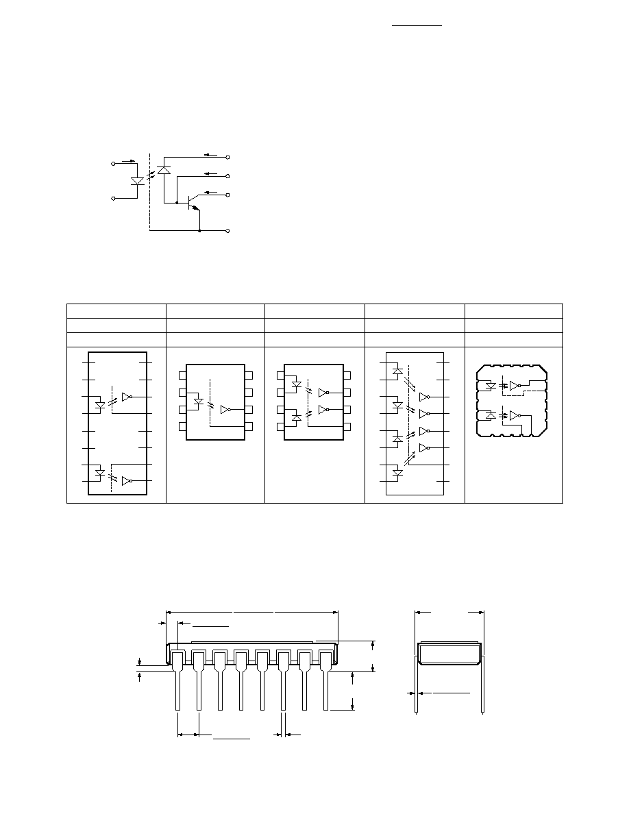
Functional Diagram
Multiple Channel Devices
Available
VCC
GND
VO
VB
*See matrix for available extensions.
4N55*
5962-87679
HCPL-553X
HCPL-653X
HCPL-257K
HCPL-655X
5962-90854
HCPL-550X
The connection of a 0.1
µ
F bypass capacitor between V
CC
and GND is recommended.

2
capability will enable the designer
to interface any TTL family to
CMOS. The availability of the
base lead allows optimized gain/
bandwidth adjustment in analog
applications. The shallow depth
of the IC photodiode provides
better radiation immunity than
conventional phototransistor
couplers.
These products are also available
with the transistor base node
connected to improve common
mode noise immunity and ESD
susceptibility. In addition, higher
CTR minimums are available by
special request.
Package styles for these parts are
8 and 16 pin DIP through hole
(case outlines P and E respec-
tively), 16 pin DIP flat pack (case
outline F), and leadless ceramic
chip carrier (case outline 2).
Devices may be purchased with a
variety of lead bend and plating
options, see Selection Guide
Table for details. Standard
Microcircuit Drawing (SMD)
parts are available for each
package and lead style.
Because the same functional die
(emitters and detectors) are used
for each channel of each device
listed in this data sheet, absolute
maximum ratings, recommended
operating conditions, electrical
specifications, and performance
characteristics shown in the
figures are identical for all parts.
Occasional exceptions exist due
to package variations and
limitations and are as noted.
Additionally, the same package
assembly processes and materials
are used in all devices. These
similarities give justification for
the use of data obtained from one
part to represent other part's
performance for die related
reliability and certain limited
radiation test results.
Selection Guide≠Package Styles and Lead Configuration Options
Package
16 Pin DIP
8 Pin DIP
8 Pin DIP
16 Pin Flat Pack
20 Pad LCCC
Lead Style
Through Hole
Through Hole
Through Hole
Unformed Leads
Surface Mount
Channels
2
1
2
4
2
Common Channel Wiring
None
None
V
CC
GND
V
CC
GND
None
Agilent Part # & Options
Commercial
4N55*
HCPL-5500
HCPL-5530
HCPL-6550
HCPL-6530
MIL-PRF-38534, Class H
4N55/883B
HCPL-5501
HCPL-5531
HCPL-6551
HCPL-6531
MIL-PRF-38534, Class K
HCPL-257K
HCPL-550K
HCPL-553K
HCPL-655K
HCPL-653K
Standard Lead Finish
Gold Plate
Gold Plate
Gold Plate
Gold Plate
Solder Pads
Solder Dipped
Option #200
Option #200
Option #200
Butt Cut/Gold Plate
Option #100
Option #100
Option #100
Gull Wing/Soldered
Option #300
Option #300
Option #300
Class H SMD Part #
Prescript for all below
5962-
5962-
5962-
5962-
5962-
Either Gold or Solder
8767901EX
9085401HPX
8767902PX
8767904FX
87679032X
Gold Plate
8767901EC
9085401HPC
8767902PC
8767904FC
Solder Dipped
8767901EA
9085401HPA
8767902PA
87679032A
Butt Cut/Gold Plate
8767901UC
9085401HYC
8767902YC
Butt Cut/Soldered
8767901UA
9085401HYA
8767902YA
Gull Wing/Soldered
8767901TA
9085401HXA
8767902XA
Prescript for all below
5962-
5962-
5962-
5962-
5962-
Either Gold or Solder
8767905KEX
9085401KPX
8767906KPX
8767908KFX
8767907K2X
Gold Plate
8767905KEC
9085401KPC
8767906KPC
8767908KFC
Solder Dipped
8767905KEA
9085401KPA
8767906KPA
8767907K2A
Butt Cut/Gold Plate
8767905KUC
9085401KYC
8767906KYC
Butt Cut/Soldered
8767905KUA
9085401KYA
8767906KYA
Gull Wing/Soldered
8767905KTA
9085401KXA
8767906KXA
*JEDEC registered part.
3
0.20 (0.008)
0.33 (0.013)
4.45 (0.175)
MAX.
20.06 (0.790)
20.83 (0.820)
0.51 (0.020)
MAX.
2.29 (0.090)
2.79 (0.110)
0.51 (0.020)
MIN.
0.89 (0.035)
1.65 (0.065)
8.13 (0.320)
MAX.
7.36 (0.290)
7.87 (0.310)
NOTE: DIMENSIONS IN MILLIMETERS (INCHES).
3.81 (0.150)
MIN.
Functional Diagrams
16 Pin DIP
8 Pin DIP
8 Pin DIP
16 Pin Flat Pack
20 Pad LCCC
Through Hole
Through Hole
Through Hole
Unformed Leads
Surface Mount
2 Channels
1 Channel
2 Channels
4 Channels
2 Channels
Note: 8 pin DIP and flat pack devices have common V
CC
and ground. 16 pin DIP and LCCC (leadless ceramic chip carrier) packages
have isolated channels with separate V
CC
and ground connections.
1
3
2
4
8
6
7
5
V
CC
GND
V
OUT
V
B
1
3
2
4
8
6
7
5
V
CC
GND
V
O2
V
O1
5
7
6
8
12
10
11
9
GND
V
O4
V
O3
1
3
2
4
16
14
15
13
V
CC
V
O2
V
O1
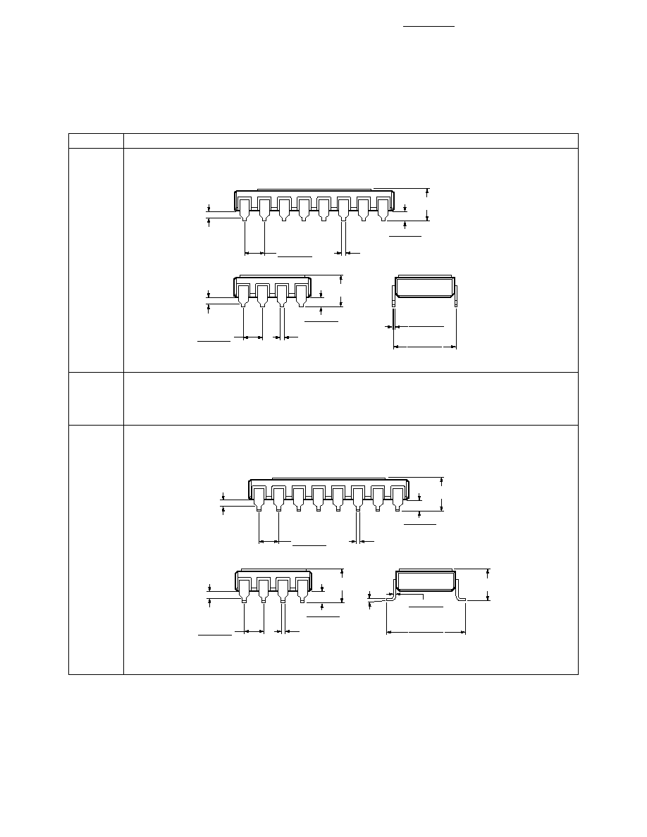
Outline Drawings
16 Pin DIP Through Hole, 2 Channels
GND1
VB2
19
20
2
3
VO1
8
7
VCC2
VCC1
10
GND2
15
13
12
14
VO2
VB1 9
ANODE
3
CATHODE
6
5
VO
GND
IO
IF
2
+
≠
VF
8
VCC
7
VB
IB
ICC
8 Pin Ceramic DIP Single
Channel Schematic
Note base pin 7.
5
7
6
8
12
10
11
9
GND
V
CC2
V
B2
1
3
2
4
16
14
15
13
V
CC1
GND
V
O1
V
O2
V
B1

4
Outline Drawings
16 Pin Flat Pack, 4 Channels
8.13 (0.320)
MAX.
5.23
(0.206)
MAX.
2.29 (0.090)
MAX.
7.24 (0.285)
6.99 (0.275)
1.27 (0.050)
REF.
0.46 (0.018)
0.36 (0.014)
11.13 (0.438)
10.72 (0.422)
2.85 (0.112)
MAX.
0.89 (0.035)
0.69 (0.027)
0.31 (0.012)
0.23 (0.009)
0.88 (0.0345)
MIN.
9.02 (0.355)
8.76 (0.345)
NOTE: DIMENSIONS IN MILLIMETERS (INCHES).
20 Terminal LCCC Surface Mount, 2
Channels
8 Pin DIP Through Hole, 1 and 2
Channel
3.81 (0.150)
MIN.
4.32 (0.170)
MAX.
9.40 (0.370)
9.91 (0.390)
0.51 (0.020)
MAX.
2.29 (0.090)
2.79 (0.110)
0.51 (0.020)
MIN.
0.76 (0.030)
1.27 (0.050)
8.13 (0.320)
MAX.
7.36 (0.290)
7.87 (0.310)
0.20 (0.008)
0.33 (0.013)
7.16 (0.282)
7.57 (0.298)
NOTE: DIMENSIONS IN MILLIMETERS (INCHES).
8.70 (0.342)
9.10 (0.358)
4.95 (0.195)
5.21 (0.205)
1.78 (0.070)
2.03 (0.080)
1.02 (0.040) (3 PLCS)
4.95 (0.195)
5.21 (0.205)
8.70 (0.342)
9.10 (0.358)
1.78 (0.070)
2.03 (0.080)
0.51 (0.020)
0.64
(0.025)
(20 PLCS)
1.52 (0.060)
2.03 (0.080)
METALIZED
CASTILLATIONS (20 PLCS)
2.16 (0.085)
TERMINAL 1 IDENTIFIER
NOTE: DIMENSIONS IN MILLIMETERS (INCHES).
SOLDER THICKNESS 0.127 (0.005) MAX.
1.14 (0.045)
1.40 (0.055)
Leaded Device Marking
Leadless Device Marking
COMPLIANCE INDICATOR,*
DATE CODE, SUFFIX (IF NEEDED)
A QYYWWZ
XXXXXX
XXXXXXX
XXX XXX
50434
COUNTRY OF MFR.
Agilent CAGE CODE*
Agilent DESIGNATOR
DSCC SMD*
PIN ONE/
ESD IDENT
Agilent P/N
DSCC SMD*
* QUALIFIED PARTS ONLY
COMPLIANCE INDICATOR,*
DATE CODE, SUFFIX (IF NEEDED)
A QYYWWZ
XXXXXX
XXXX
XXXXXX
XXX 50434
DSCC SMD*
Agilent CAGE CODE*
Agilent DESIGNATOR
COUNTRY OF MFR.
Agilent P/N
PIN ONE/
ESD IDENT
DSCC SMD*
* QUALIFIED PARTS ONLY
5
Hermetic Optocoupler Options
Option
Description
100
Surface mountable hermetic optocoupler with leads trimmed for butt joint assembly. This
option is available on commercial and hi-rel product in 8 and 16 pin DIP (see drawings below
for details).
200
Lead finish is solder dipped rather than gold plated. This option is available on commercial
and hi-rel product in 8 and 16 pin DIP. DSCC drawing part numbers contain provisions for
lead finish. All leadless chip carrier devices are delivered with solder dipped terminals as a
standard feature.
300
Surface mountable hermetic optocoupler with leads cut and bent for gull wing assembly. This
option is available on commercial and hi-rel product in 8 and 16 pin DIP (see drawings below
for details). This option has solder dipped leads.
1.14 (0.045)
1.40 (0.055)
4.32 (0.170)
MAX.
0.51 (0.020)
MAX.
2.29 (0.090)
2.79 (0.110)
0.51 (0.020)
MIN.
7.36 (0.290)
7.87 (0.310)
0.20 (0.008)
0.33 (0.013)
NOTE: DIMENSIONS IN MILLIMETERS (INCHES).
1.14 (0.045)
1.40 (0.055)
4.32 (0.170)
MAX.
0.51 (0.020)
MAX.
2.29 (0.090)
2.79 (0.110)
0.51 (0.020)
MIN.
1.40 (0.055)
1.65 (0.065)
4.57 (0.180)
MAX.
0.51 (0.020)
MAX.
2.29 (0.090)
2.79 (0.110)
0.51 (0.020)
MIN.
0.51 (0.020)
MIN.
4.57 (0.180)
MAX.
0.51 (0.020)
MAX.
2.29 (0.090)
2.79 (0.110)
1.40 (0.055)
1.65 (0.065)
9.65 (0.380)
9.91 (0.390)
5∞ MAX.
4.57 (0.180)
MAX.
NOTE: DIMENSIONS IN MILLIMETERS (INCHES).
0.20 (0.008)
0.33 (0.013)