Document Outline
- HSMP-381x, -481x Series
- Features
- Description/Applications
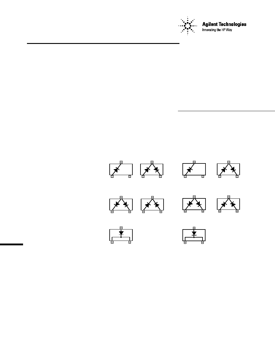
- Package Lead Code Identification
- Absolute Maximum Ratings
- Electrical Specifications
- Typical Parameters
- Typical Applications for Multiple Diode Products
- Typical Applications for HSMP-481x Low Inductance Series
- Equivalent Circuit Model
- Assembly Information
- Package Dimensions
- Package Characteristics
- Ordering Information
- Device Orientation
- Tape Dimensions
Surface Mount RF PIN Low
Distortion Attenuator Diodes
Technical Data
Features
∑ Diodes Optimized for:
≠ Low Distortion Attenuating
≠ Microwave Frequency
Operation
∑ Surface Mount Packages
≠ Single and Dual Versions
≠ Tape and Reel Options
Available
∑ Low Failure in Time (FIT)
Rate
[1]
Note:
1. For more information see the
Surface Mount PIN Reliability Data
Sheet.
HSMP-381x Series and
HSMP-481x Series
Package Lead Code
Identification, SOT-23
(Top View)
Description/Applications
The HSMP-381x series is
specifically designed for low
distortion attenuator applica-
tions. The HSMP-481x products
feature ultra low parasitic
inductance in the SOT-23 and
SOT-323 packages. They are
specifically designed for use at
frequencies which are much
higher than the upper limit for
conventional diodes.
A SPICE model is not available
for PIN diodes as SPICE does not
provide for a key PIN diode
characteristic, carrier lifetime.
COMMON
CATHODE
#4
COMMON
ANODE
#3
SERIES
#2
SINGLE
#0
1
2
3
1
2
3
1
2
3
1
2
3
4810
1
2
3
DUAL CATHODE
Package Lead Code
Identification, SOT-323
(Top View)
COMMON
CATHODE
F
COMMON
ANODE
E
SERIES
C
SINGLE
B
481B
DUAL CATHODE
2
Absolute Maximum Ratings
[1]
T
C
= +25
∞
C
Symbol
Parameter
Unit
SOT-23
SOT-323
I
f
Forward Current (1
µ
s Pulse) Amp
1
1
P
IV
Peak Inverse Voltage
V
Same as V
BR
Same as V
BR
T
j
Junction Temperature
∞
C
150
150
T
stg
Storage Temperature
∞
C
-65 to 150
-65 to 150
jc
Thermal Resistance
[2]
∞
C/W
500
150
Notes:
1. Operation in excess of any one of these conditions may result in permanent damage to
the device.
2. T
C
= +25
∞
C, where T
C
is defined to be the temperature at the package pins where
contact is made to the circuit board.
Electrical Specifications T
C
= +25
∞
C (Each Diode)
Conventional Diodes
Minimum
Maximum
Maximum
Minimum
Maximum
Part
Package
Breakdown
Total
Total
High
Low
Number
Marking
Lead
Voltage
Resistance Capacitance
Resistance
Resistance
HSMP-
Code
Code
Configuration
V
BR
(V)
R
T
(
)
C
T
(pF)
R
H
(
)
R
L
(
)
3810
E0
[1]
0
Single
100
3.0
0.35
1500
10
3812
E2
[1]
2
Series
3813
E3
[1]
3
Common Anode
3814
E4
[1]
4
Common Cathode
381B
E0
[2]
B
Single
381C
E2
[2]
C
Series
381E
E3
[2]
E
Common Anode
381F
E4
[2]
F
Common Cathode
Test Conditions
V
R
= V
BR
I
F
= 100 mA
V
R
= 50 V
I
R
= 0.01 mA
I
F
= 20 mA
Measure
f = 100 MHz
f = 1 MHz
f = 100 MHz
f= 100 MHz
I
R
10
µ
A
High Frequency (Low Inductance, 500 MHz ≠ 3 GHz) PIN Diodes
Minimum
Maximum
Typical
Maximum
Typical
Part
Package
Breakdown
Series
Total
Total
Total
Number
Marking
Lead
Voltage
Resistance Capacitance Capacitance Inductance
HSMP-
Code
Code
Configuration
V
BR
(V)
R
S
(
)
C
T
(pF)
C
T
(pF)
L
T
(nH)
4810
EB
B
[1]
Dual Cathode
100
3.0
0.35
0.4
1.0
481B
EB
B
[2]
Dual Cathode
Test Conditions
V
R
= V
BR
I
F
= 100 mA
V
R
= 50 V
V
R
= 50 V
f = 500 MHz ≠
Measure
f = 1 MHz
f = 1 MHz
3 GHz
I
R
10
µ
A
V
R
= 0 V
Notes:
1. Package marking code is white.
2. Package laser marked.
3
Typical Parameters at T
C
= 25
∞
C
Part Number
Series Resistance
Carrier Lifetime
Reverse Recovery Time
Total Capacitance
HSMP-
R
S
(
)
(ns)
T
rr
(ns)
C
T
(pF)
381x
75
1500
300
0.27 @ 50 V
Test Conditions
I
F
= 1 mA
I
F
= 50 mA
V
R
= 10 V
f = 1 MHz
f = 100 MHz
I
R
= 250 mA
I
F
= 20 mA
90% Recovery
Typical Parameters at T
C
= 25
∞
C (unless otherwise noted), Single Diode
10000
1000
100
10
1
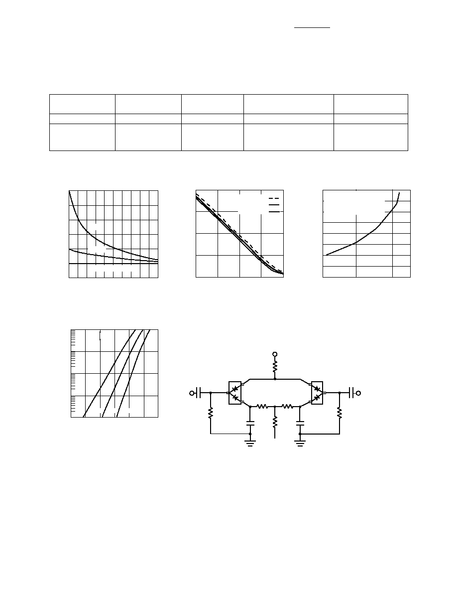
RF RESISTANCE (OHMS)
0.01
0.1
1
10
100
I
F
≠ FORWARD BIAS CURRENT (mA)
T
A
= +85
∞
C
T
A
= +25
∞
C
T
A
= ≠55
∞
C
Figure 2. RF Resistance vs. Forward
Bias Current.
0.15
0.30
0.25
0.20
0.35
0.40
0.45
0
2
6
4
10 12
8
16
14
18 20
TOTAL CAPACITANCE (pF)
REVERSE VOLTAGE (V)
Figure 1. RF Capacitance vs. Reverse
Bias.
1 MHz
30 MHz
frequency>100 MHz
120
110
100
90
80
70
60
50
40
1000
100
10
Diode Mounted as a
Series Attenuator
in a 50 Ohm Microstrip
and Tested at 123 MHz
DIODE RF RESISTANCE (OHMS)
Figure 3. 2nd Harmonic Input
Intercept Point vs. Diode RF
Resistance.
INPUT INTERCEPT POINT (dBm)
100
10
1
0.1
0.01
0
0.2
0.4
0.6
0.8
1.0
1.2
I
F
≠ FORWARD CURRENT (mA)
V
F
≠ FORWARD VOLTAGE (mA)
Figure 4. Forward Current vs.
Forward Voltage.
125
∞
C 25
∞
C ≠50
∞
C
INPUT
RF IN/OUT
Figure 5. Four Diode
Attenuator. See Application Note 1048
for Details.
FIXED
BIAS
VOLTAGE
VARIABLE BIAS
Typical Applications for Multiple Diode Products

4
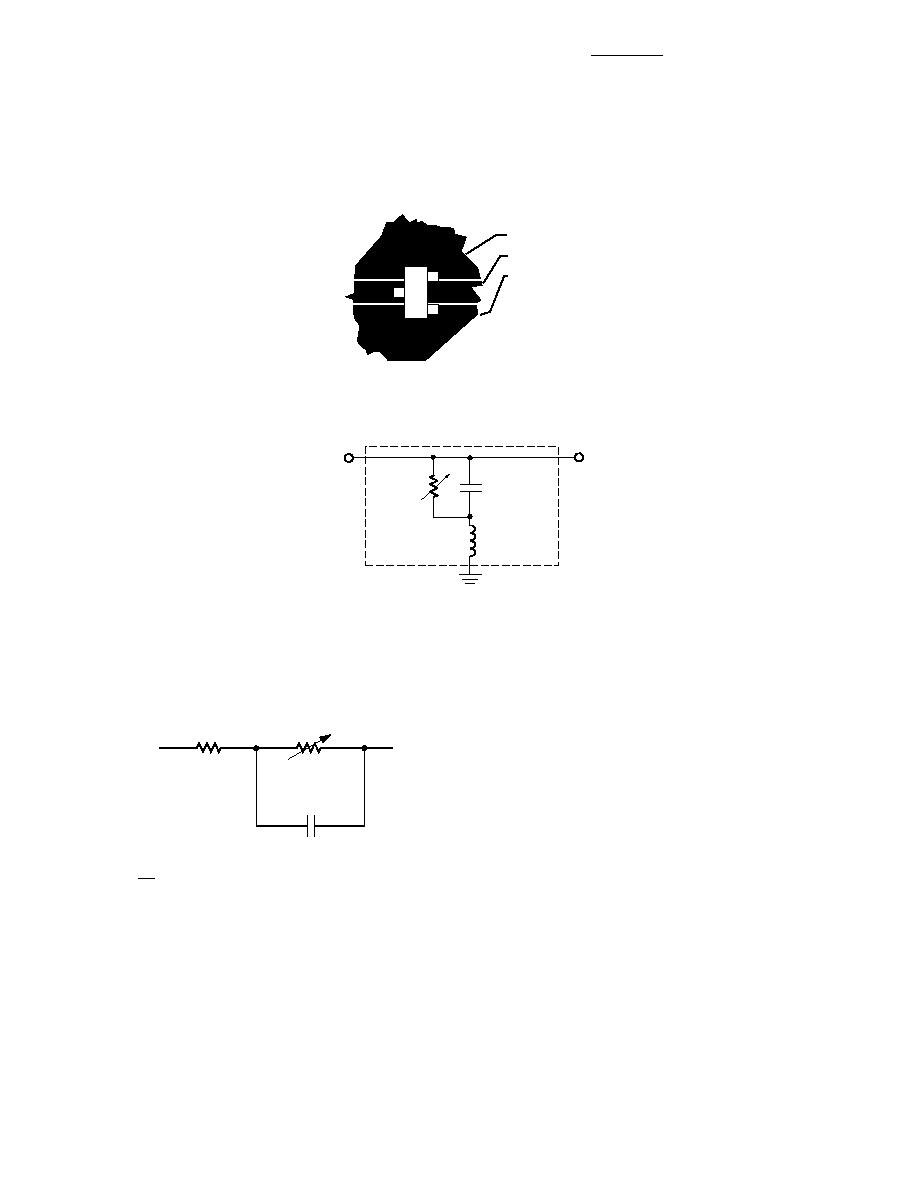
Typical Applications for HSMP-481x Low Inductance Series
Microstrip Series
Connection for
HSMP-481x Series
In order to take full advantage of
the low inductance of the
HSMP-481x series when using
them in series applications,
both lead 1 and lead 2 should be
connected together, as shown in
Figure 7.
Figure 7. Circuit Layout.
0.3 nH
0.3 nH
0.3 pF
R
j
1.5 nH
1.5 nH
Figure 9. Equivalent Circuit.
R
j
0.08
+ 2.5
I
b
0.9
1
2
3
Figure 6. Internal Connections.
HSMP-481x
Microstrip Shunt
Connections for
HSMP-481x Series
In Figure 8, the center
conductor of the microstrip
line is interrupted and
leads 1 and 2 of the
HSMP-481x series diode are
placed across the resulting gap.
This forces the 1.5 nH lead
inductance of leads 1 and 2 to
appear as part of a low pass
filter, reducing the shunt
parasitic inductance and
increasing the maximum
available attenuation. The
0.3 nHof shunt inductance
external to the diode is created
by the via holes, and is a good
estimate for 0.032" thick material.
50 OHM MICROSTRIP LINES
PAD CONNECTED TO
GROUND BY TWO
VIA HOLES
Figure 8. Circuit Layout.
5
Typical Applications for HSMP-481x Low Inductance Series (continued)
Figure 10. Circuit Layout.
Co-Planar Waveguide
Groundplane
Center Conductor
Groundplane
Co-Planar Waveguide
Shunt Connection for
HSMP-481x Series
Co-Planar waveguide, with
ground on the top side of the
printed circuit board, is shown
in Figure 10. Since it eliminates
the need for via holes to ground,
it offers lower shunt parasitic
inductance and higher maximum
attenuation when compared to a
microstrip circuit.
Figure 11. Equivalent Circuit.
0.3 pF
0.75 nH
R
j
0.18 pF*
* Measured at -20 V
2.5
R
j
R
s
C
j
R
j
=
80
I
0.9
R
T
= 2.5 + R
j
C
T
= C
P
+ C
j
I
= Forward Bias Current in mA
*See AN1124 for package models.
Equivalent Circuit Model
HSMS-381x Chip*