Document Outline
- HSMS-28XX Series
- Features
- Description/Applications
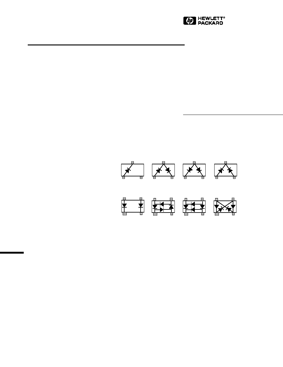
- Package Lead Code Identification
- Electrical Specifications
- Absolute Maximum Ratings
- Quad Capacitance
- SPICE Parameters
- Typical Parameters
- Applications Information
- Profile Option Descriptions
- Ordering Information
- Package Characteristics
- Package Dimensions
- Device Orientation
Surface Mount RF Schottky
Barrier Diodes
Technical Data
HSMS-28XX Series
Features
∑ Surface Mount SOT-23/SOT-
143 Package
∑ Low Turn-On Voltage
(As Low as 0.34 V at 1 mA)
∑ Low FIT (Failure in Time)
Rate*
∑ Six-sigma Quality Level
∑ Single, Dual and Quad
Versions
∑ Tape and Reel Options
Available
*
For more information see the
Surface Mount Schottky Reliability
Data Sheet.
Description/Applications
These Schottky diodes are
specifically designed for both
analog and digital applications.
This series offers a wide range of
specifications and package
configurations to give the
designer wide flexibility. Typical
applications of these Schottky
diodes are mixing, detecting,
switching, sampling, clamping,
and wave shaping. The
HSMS-2800 series of diodes is
optimized for high voltage
applications. The HSMS-2810
series of diodes features very low
flicker (1/f) noise. The
Package Lead Code Identification
TOP VIEW
COMMON
CATHODE
#4
UNCONNECTED
PAIR
#5
COMMON
ANODE
#3
SERIES
#2
SINGLE
#0
1
2
3
1
2
3
4
RING
QUAD
#7
1
2
3
4
BRIDGE
QUAD
#8
1
2
3
4
CROSS-OVER
QUAD
#9
1
2
3
4
1
2
3
1
2
3
1
2
3
HSMS-2820 series of diodes is the
best all-around choice for most
applications, featuring low series
resistance, low forward voltage at
all current levels and good RF
characteristics. The HSMS-2860
series is a high performance
diode offering superior V
f
and
ultra-low capacitance.
Note that HP's manufacturing
techniques assure that dice found
in pairs and quads are taken from
adjacent sites on the wafer,
assuring the highest degree of
match.

2
Electrical Specifications T
A
= 25
∞
C, Single Diode
[4]
Nearest
Minimum
Maxi-
Maximum
Maximum
Maxi-
Typical
Part
Package
Equivalent
Break-
mum
Forward
Reverse
mum
Dynamic
Num-
Mark-
Axial Lead
down
Forward
Voltage
Leakage
Capac-
Resis-
ber
ing
Lead
Part No.
Voltage
Voltage
V
F
(V) @
I
R
(nA) @
itance
tance
HSMS
[5]
Code
[3]
Code
Configuration
5082-
V
BR
(V)
V
F
(mV)
I
F
(mA)
V
R
(V)
C
T
(pF)
R
D
(
)
[6]
2800
A0
0
Single
2800
70
400
1.0
15
200
50
2.0
35
(1N5711)
2802
A2
2
Series
2803
A3
3
Common Anode
2804
A4
4
Common
Cathode
2805
A5
5
Unconnected
Pair
2807
A7
7
Ring Quad
[6]
2808
A8
8
Bridge Quad
[6]
2810
B0
0
Single
2810
20
400
1.0
35
200
15
1.2
15
(1N5712)
2812
B2
2
Series
2813
B3
3
Common Anode
2814
B4
4
Common
Cathode
2815
B5
5
Unconnected
Pair
2817
B7
7
Ring Quad
[6]
2818
B8
8
Bridge Quad
[6]
2820
C0
0
Single
2835
15*
340
0.7
30
100
1
1.0
12
2822
C2
2
Series
2823
C3
3
Common Anode
2824
C4
4
Common
Cathode
2825
C5
5
Unconnected
Pair
2827
C7
7
Ring Quad
[6]
2828
C8
8
Bridge Quad
[6]
2829
C9
9
Cross-over Quad
2860
T0
0
Single
None
4
350
0.6
30
--
0.35
10
2862
T1
2
Series Pair
2863
T3
3
Common Anode
2864
T4
4
Common
Cathode
2865
T5
5
Unconnected
Pair
Test Conditions
I
R
= 10
µ
A
I
F
=
V
F
= 0 V
I
F
= 5 mA
*I
R
=
1 mA
[1]
f =
100
µ
A
1.0 MHz
[2]
Notes:
1.
V
F
for diodes in pairs and quads in 15 mV maximum at 1 mA.
2.
C
TO
for diodes in pairs and quads is 0.2 pF maximum.
3. Package marking code is in white.
4. Effective Carrier Lifetime (
) for all these diodes is 100 ps maximum measured with Krakauer method at 5 mA, except HSMS-282X which
is measured at 20 mA.
5. See section titled "Quad Capacitance."
6. R
D
= R
S
+ 5.2
at 25
∞
C and I
f
= 5 mA.

3
Absolute Maximum Ratings
[1]
T
A
= 25
∞
C
Symbol
Parameter
Value
I
f
Forward Current (1 ms Pulse)
1 Amp
P
t
Total Device Dissipation
250 mW
[2]
P
IV
Peak Inverse Voltage
Same as V
BR
T
j
Junction Temperature
150
∞
C
T
stg
Storage Temperature
-65 to 150
∞
C
Notes:
1. Operation in excess of any one of these conditions may result in permanent
damage to this device.
2. CW Power Dissipation at T
LEAD
= 25
∞
C. Derate to zero at maximum rated
temperature.
Quad Capacitance
Capacitance of Schottky diode
quads is measured using an
HP4271 LCR meter. This
instrument effectively isolates
individual diode branches from
the others, allowing accurate
capacitance measurement of each
branch or each diode. The
conditions are: 20 mV R.M.S.
voltage at 1 MHz. HP defines this
measurement as "CM", and it is
equivalent to the capacitance of
the diode by itself. The equivalent
diagonal and adjacent
capacitances can then be
calculated by the formulas given
below.
In a quad, the diagonal capaci-
tance is the capacitance between
points A and B as shown in the
figure below. The diagonal
capacitance is calculated using
the following formula
C
1
x C
2
C
3
x C
4
C
DIAGONAL
= _______ + _______
C
1
+ C
2
C
3
+ C
4
C
1
C
2
C
4
C
3
A
B
C
The equivalent adjacent
capacitance is the capacitance
between points A and C in the
figure below. This capacitance is
calculated using the following
formula
1
C
ADJACENT
= C
1
+ ____________
1
1
1
≠≠ + ≠≠ + ≠≠
C
2
C
3
C
4
This information does not apply
to cross-over quad diodes.
SPICE Parameters
Parameter
Units
HSMS-280X
HSMS-281X
HSMS-282X
HSMS-286X
B
V
V
75
25
15
7.0
C
J0
pF
1.6
1.1
0.7
0.18
E
G
eV
0.69
0.69
0.69
0.69
I
BV
A
10E-5
10E-5
10E-4
10E-5
I
S
A
3 x 10E - 8
4.8 x 10E - 9
2.2 x 10E -8
5.0 x 10E -8
N
1.08
1.08
1.08
1.08
R
S
30
10
6.0
5.0
P
B
V
0.65
0.65
0.65
0.65
P
T
2
2
2
2
M
0.5
0.5
0.5
0.5
4
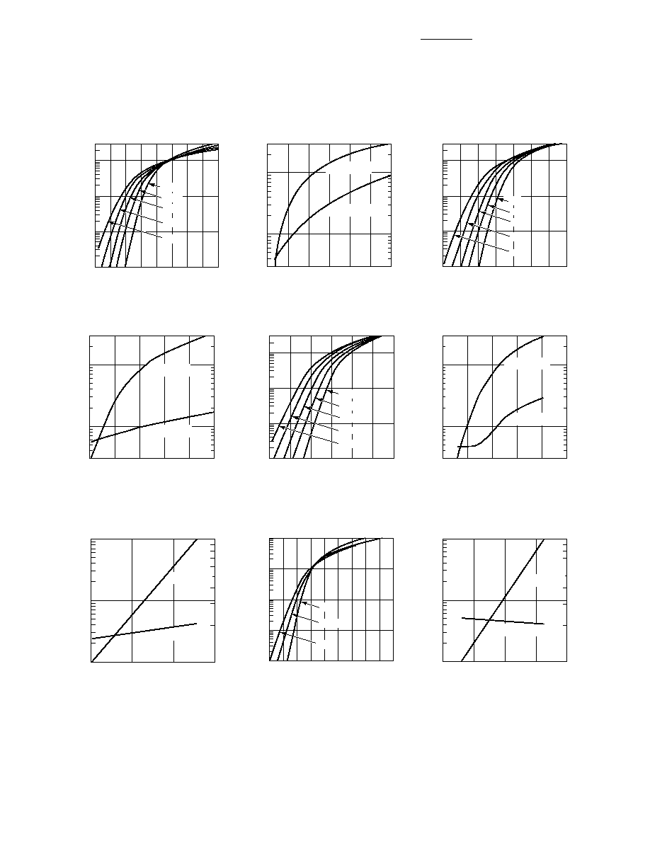
Typical Parameters at T
A
= 25
∞
C (unless otherwise noted), Single Diode
V
F
- FORWARD VOLTAGE (V)
Figure 1. Typical Forward Current vs.
Forward Voltage at Temperatures--
HSMS-2800 Series
30
10
1
0.1
0.01
I
F
- FORWARD CURRENT (mA)
0.1 0.2 0.3 0.4 0.5
0.6 0.7 0.8
0.9
55
∞
C
85
∞
C
≠35
∞
C
25
∞
C
≠5
∞
C
V
F
- FORWARD VOLTAGE (V)
Figure 2. Typical V
f
Match, HSMS-2800
Series Pairs and Quads.
30
10
1
0.3
30
10
1
0.3
I
F
- FORWARD CURRENT (mA)
V
F
- FORWARD VOLTAGE DIFFERENCE (mV)
0.2
0.4
0.6
0.8
1.0
1.2
1.4
I
F
(Left Scale)
V
F
(Right Scale)
V
F
- FORWARD VOLTAGE (V)
Figure 3. Typical Forward Current vs.
Forward Voltage at Temperatures--
HSMS-2810 Series.
30
10
1
0.1
0.01
I
F
- FORWARD CURRENT (mA)
0.1
0.2
0.3
0.4
0.5
0.6
0.7
0.8
V
F
- FORWARD VOLTAGE (V)
Figure 4. Typical V
f
Match, HSMS-2810
Series Pairs and Quads.
30
10
1
0.3
30
10
1
0.3
I
F
- FORWARD CURRENT (mA)
V
F
- FORWARD VOLTAGE DIFFERENCE (mV)
0.3
0.4
0.5
0.5
0.6
0.7
I
F
(Left Scale)
V
F
(Right Scale)
V
F
- FORWARD VOLTAGE (V)
Figure 5. Typical Forward Current vs.
Forward Voltage At Temperatures--
HSMS-2820 Series.
30
10
1
0.1
0.01
I
F
- FORWARD CURRENT (mA)
0.1
0.2
0.3
0.4
0.5
0.6
0.7
V
F
- FORWARD VOLTAGE (V)
Figure 6. Typical V
f
Match, HSMS-2820
Series Pairs and Quads at Mixer Bias
Levels.
30
10
1
0.3
30
10
1
0.3
I
F
- FORWARD CURRENT (mA)
V
F
- FORWARD VOLTAGE DIFFERENCE (mV)
0.2
0.4
0.6
0.8
1.0
1.2
1.4
I
F
(Left Scale)
V
F
(Right Scale)
V
F
- FORWARD VOLTAGE (V)
Figure 7. Typical V
f
Match, HSMS-2820
Series Pairs at Detector Bias Levels.
100
10
1
1.0
0.1
I
F
- FORWARD CURRENT (
µ
A)
V
F
- FORWARD VOLTAGE DIFFERENCE (mV)
0.10
0.15
0.20
0.25
I
F
(Left Scale)
V
F
(Right Scale)
FORWARD VOLTAGE (V)
Figure 8. Typical Forward Current vs.
Forward Voltage at Temperature,
HSMS-2860 Series.
100
10
1
0.1
0.01
FORWARD CURRENT (mA)
0.1 0.2 0.3 0.4 0.5 0.6 0.7 0.8 0.9 1.0
≠55
∞
C
25
∞
C
V
F
- FORWARD VOLTAGE (V)
Figure 9. Typical V
f
Match, HSMS-2860
Series Pairs at Detector Bias Levels.
100
10
1
10
1.0
I
F
- FORWARD CURRENT (
µ
A)
V
F
- FORWARD VOLTAGE DIFFERENCE (mV)
0.05
0.10
0.20
0.15
0.25
I
F
(Left Scale)
V
F
(Right Scale)
55
∞
C
85
∞
C
≠35
∞
C
25
∞
C
≠5
∞
C
55
∞
C
85
∞
C
≠35
∞
C
25
∞
C
≠55
∞
C
85
∞
C
5
Typical Parameters,
continued
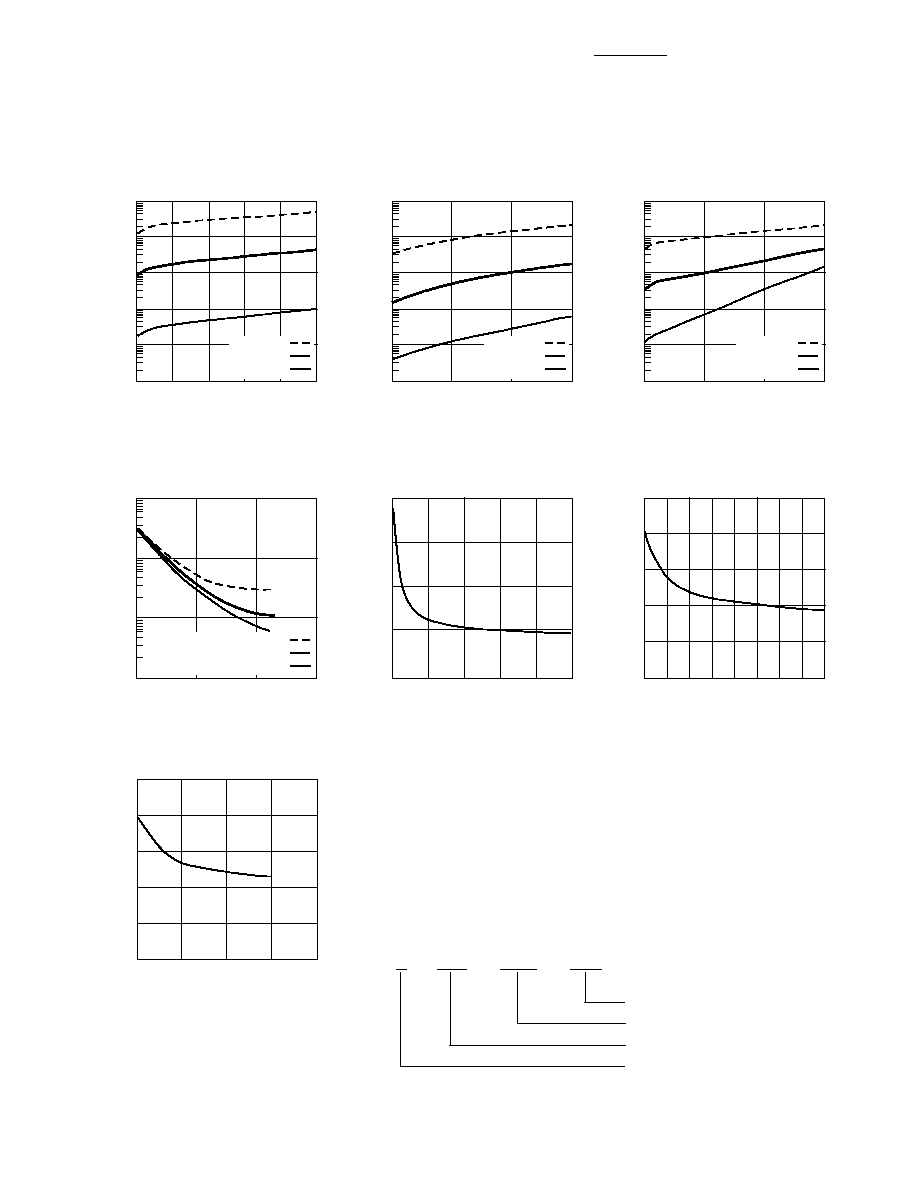
Figure 10. Reverse Current vs.
Reverse Voltage at Temperatures--
HSMS-2800 Series.
0
10
20
30
50
40
I
R
≠ REVERSE CURRENT (nA)
V
R
≠ REVERSE VOLTAGE (V)
1
1000
100
10
100,000
10,000
T
A
= +125
∞
C
T
A
= +75
∞
C
T
A
= +25
∞
C
Figure 11. Reverse Current vs.
Reverse Voltage at Temperatures--
HSMS-2810 Series.
0
5
15
I
R
≠ REVERSE CURRENT (nA)
V
R
≠ REVERSE VOLTAGE (V)
10
1
1000
100
10
100,000
10,000
T
A
= +125
∞
C
T
A
= +75
∞
C
T
A
= +25
∞
C
Figure 12. Reverse Current vs.
Reverse Voltage at Temperatures--
HSMS-2820 Series.
0
2
6
I
R
≠ REVERSE CURRENT (nA)
V
R
≠ REVERSE VOLTAGE (V)
4
1
1000
100
10
100,000
10,000
T
A
= +125
∞
C
T
A
= +75
∞
C
T
A
= +25
∞
C
Figure 13. Dynamic Resistance vs.
Forward Current--HSMS-2800 Series.
0.1
1
100
R
D
≠ DYNAMIC RESISTANCE (
)
I
F
≠ FORWARD CURRENT (mA)
10
1
10
1000
100
HSMS-2800 SERIES
HSMS-2810 SERIES
HSMS-2820 SERIES
Figure 14. Total Capacitance vs.
Reverse Voltage--HSMS-2800 Series.
0
10
20
30
50
40
C
T
≠ CAPACITANCE (pF)
V
R
≠ REVERSE VOLTAGE (V)
0
1.5
1
0.5
2
Figure 15. Total Capacitance vs.
Reverse Voltage--HSMS-2810 Series.
0
2
6
4
10
12
8
16
14
C
T
≠ CAPACITANCE (pF)
V
R
≠ REVERSE VOLTAGE (V)
0
0.75
0.50
0.25
1.25
1
Figure 16. Total Capacitance vs.
Reverse Voltage--HSMS-2820 Series.
0
2
8
6
C
T
≠ CAPACITANCE (pF)
V
R
≠ REVERSE VOLTAGE (V)
4
0
0.6
0.4
0.2
1
0.8
Applications Information
Schottky Diode Fundamentals
See the HSMS-280A series data sheet.
Profile Option Descriptions
-BLK = Bulk
-TR1 = 3K pc. Tape and Reel, Device Orientation; See Figures 17 and 18
-TR2 = 10K pc. Tape and Reel, Device Orientation; See Figures 17 and 18
Tape and Reeling conforms to Electronic Industries RS-481, "Taping of
Surface Mounted Components for Automated Placement."
Ordering Information
Specify part number followed by option under. For example:
H
SMS
-
28XX -
XXX
Bulk or Tape and Reel Option
Part Number
Surface Mount Schottky
Hewlett-Packard
www.hp.com/go/rf
For technical assistance or the location of
your nearest Hewlett-Packard sales office,
distributor or representative call:
Americas/Canada:
1-800-235-0312 or
408-654-8675
Far East/Australasia:
Call your local HP
sales office.
Japan:
(81 3) 3335-8152
Europe:
Call your local HP sales office.
Data subject to change.
Copyright © 1999 Hewlett-Packard Co.
Obsoletes 5968-3887E
5968-5934E (6/99)
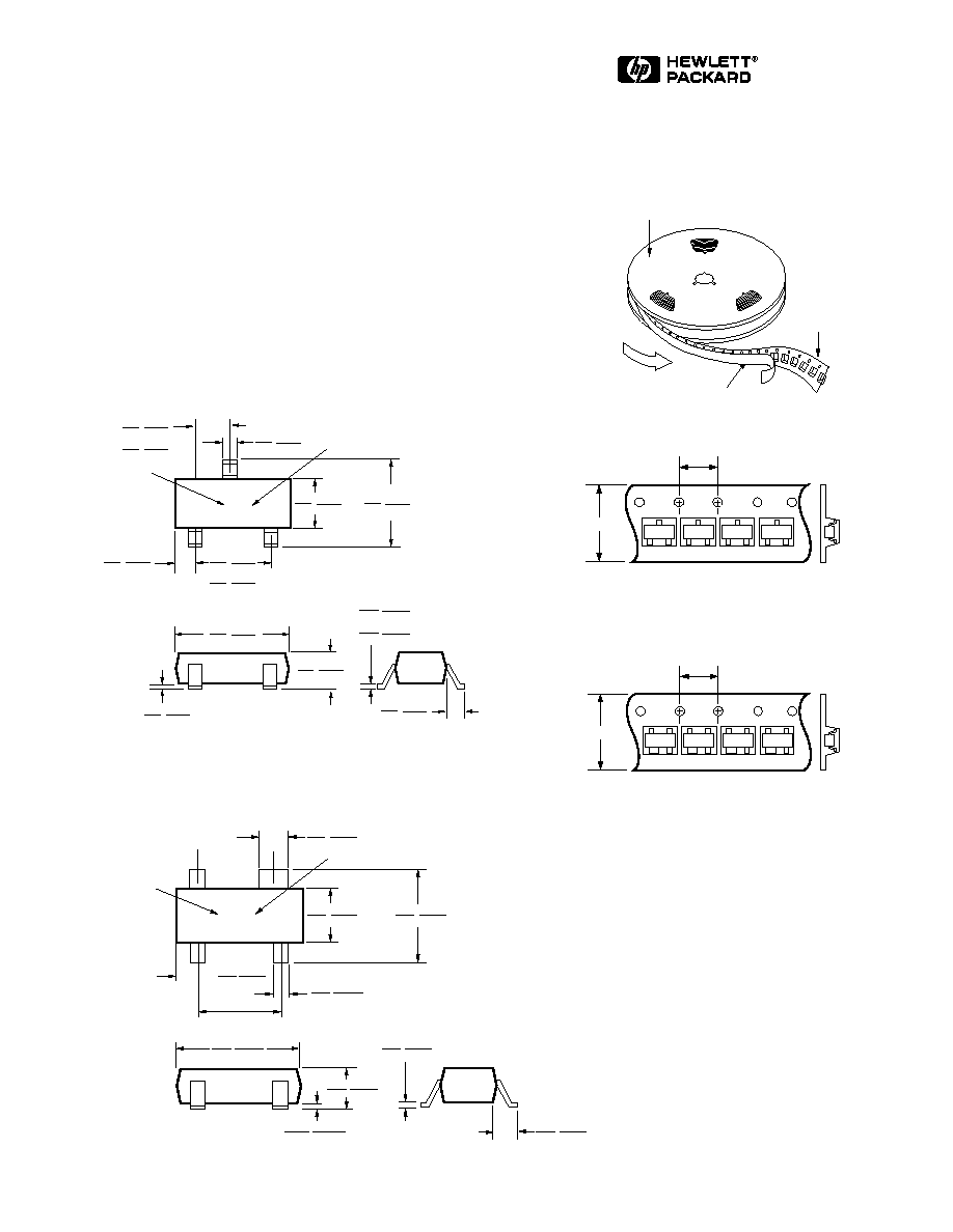
Package Dimensions
Package Characteristics
Lead Material ......................................... Alloy 42
Lead Finish ............................... Tin-Lead 85/15%
Max. Soldering Temperature .... 260
∞
C for 5 sec
Min. Lead Strength ....................... 2 pounds pull
Typical Package
Inductance ................... 2 nH (opposite leads)
Typical Package
Capacitance ............ 0.08 pF (opposite leads)
Outline 23 (SOT-23)
Outline 143 (SOT-143)
Figure 18. Options -TR1, -TR2 for SOT-143
Packages.
Figure 17. Options -TR1, -TR2 for SOT-23
Packages.
USER
FEED
DIRECTION
COVER TAPE
CARRIER
TAPE
REEL
Device Orientation
3
1
2
X X X
PACKAGE
MARKING
CODE (XX)
DATE CODE (X)
SIDE VIEW
TOP VIEW
END VIEW
THESE DIMENSIONS FOR HSMS-280X AND -281X FAMILIES ONLY.
DIMENSIONS ARE IN MILLIMETERS (INCHES)
1.02 (0.040)
0.89 (0.035)
1.03 (0.041)
0.89 (0.035)
0.60 (0.024)
0.45 (0.018)
1.40 (0.055)
1.20 (0.047)
2.65 (0.104)
2.10 (0.083)
3.06 (0.120)
2.80 (0.110)
2.04 (0.080)
1.78 (0.070)
2.05 (0.080)
1.78 (0.070)
1.04 (0.041)
0.85 (0.033)
0.152 (0.006)
0.086 (0.003)
0.180 (0.007)
0.085 (0.003)
0.10 (0.004)
0.013 (0.0005)
0.69 (0.027)
0.45 (0.018)
0.54 (0.021)
0.37 (0.015)
*
*
*
*
END VIEW
8 mm
4 mm
TOP VIEW
0.69 (0.027)
0.45 (0.018)
1.40 (0.055)
1.20 (0.047)
2.65 (0.104)
2.10 (0.083)
0.60 (0.024)
0.45 (0.018)
0.54 (0.021)
0.37 (0.015)
0.10 (0.004)
0.013 (0.0005)
1.04 (0.041)
0.85 (0.033)
0.92 (0.036)
0.78 (0.031)
2.04 (0.080)
1.78 (0.070)
DIMENSIONS ARE IN MILLIMETERS (INCHES)
0.15 (0.006)
0.09 (0.003)
3.06 (0.120)
2.80 (0.110)
PACKAGE
MARKING
CODE (XX)
B
E
C
E
X X X
DATE CODE (X)
END VIEW
8 mm
4 mm
TOP VIEW