Äîêóìåíòàöèÿ è îïèñàíèÿ www.docs.chipfind.ru

Surface Mount RF Schottky
Barrier Diodes
Technical Data
HSMS-281x Series
Features
· Surface Mount Packages
· Low Flicker Noise
· Low FIT (Failure in Time)
Rate*
· Six-sigma Quality Level
· Single, Dual and Quad
Versions
· Tape and Reel Options
Available
· Lead-free Option Available
*
For more information see the
Surface Mount Schottky Reliability
Data Sheet.
Description/Applications
These Schottky diodes are
specifically designed for both
analog and digital applications.
This series offers a wide range of
specifications and package
configurations to give the
designer wide flexibility. The
HSMS-281x series of diodes
features very low flicker (1/f)
noise.
Note that Agilent's manufacturing
techniques assure that dice found
in pairs and quads are taken from
adjacent sites on the wafer,
assuring the highest degree of
match.
Package Lead Code Identification, SOT-23/SOT-143
(Top View)
COMMON
CATHODE
#4
UNCONNECTED
PAIR
#5
COMMON
ANODE
#3
SERIES
#2
SINGLE
#0
1
2
3
1
2
3
4
RING
QUAD
#7
1
2
3
4
BRIDGE
QUAD
#8
1
2
3
4
1
2
3
1
2
3
1
2
3
Package Lead Code
Identification, SOT-323
(Top View)
Package Lead Code
Identification, SOT-363
(Top View)
COMMON
CATHODE
F
COMMON
ANODE
E
SERIES
C
SINGLE
B
UNCONNECTED
TRIO
L
1
2
3
6
5
4
HIGH ISOLATION
UNCONNECTED PAIR
K
1
2
3
6
5
4
Notes:
1. Package marking provides
orientation and identification.
2. See "Electrical Specifications" for
appropriate package marking.
Pin Connections and
Package Marking
GUx
1
2
3
6
5
4
2
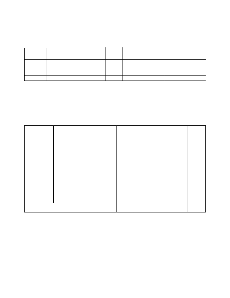
Electrical Specifications T
C
= 25
°
C, Single Diode
[4]
Maximum
Maximum
Minimum
Maximum
Forward
Reverse
Typical
Part
Package
Breakdown
Forward
Voltage
Leakage
Maximum
Dynamic
Number
Marking
Lead
Voltage
Voltage
V
F
(V) @
I
R
(nA) @
Capacitance Resistance
HSMS
[5]
Code
Code
Configuration
V
BR
(V)
V
F
(mV)
I
F
(mA)
V
R
(V)
C
T
(pF)
R
D
(
)
[6]
2810
B0
[3]
0
Single
20
400
1.0
35
200
15
1.2
15
2812
B2
[3]
2
Series
2813
B3
[3]
3
Common Anode
2814
B4
[3]
4
Common Cathode
2815
B5
[3]
5
Unconnected Pair
2817
B7
[3]
7
Ring Quad
[5]
2818
B8
[3]
8
Bridge Quad
[5]
281B
B0
[7]
B
Single
281C
B2
[7]
C
Series
281E
B3
[7]
E
Common Anode
281F
B4
[7]
F
Common Cathode
281K
BK
[7]
K
High Isolation
Unconnected Pair
281L
BL
[7]
L
Unconnected Trio
Test Conditions
I
R
= 10
µA
I
F
= 1 mA
V
F
= 0 V
I
F
= 5 mA
f = 1 MHz
Notes:
1.
V
F
for diodes in pairs and quads in 15 mV maximum at 1 mA.
2.
C
TO
for diodes in pairs and quads is 0.2 pF maximum.
3. Package marking code is in white.
4. Effective Carrier Lifetime (
) for all these diodes is 100 ps maximum measured with Krakauer method at 5 mA.
5. See section titled "Quad Capacitance."
6. R
D
= R
S
+ 5.2
at 25°C and I
f
= 5 mA.
7. Package marking code is laser marked.
Absolute Maximum Ratings
[1]
T
C
= 25
°C
Symbol
Parameter
Unit
SOT-23/SOT-143
SOT-323/ SOT-363
I
f
Forward Current (1
µs Pulse)
Amp
1
1
P
IV
Peak Inverse Voltage
V
Same as V
BR
Same as V
BR
T
j
Junction Temperature
°C
150
150
T
stg
Storage Temperature
°C
-65 to 150
-65 to 150
jc
Thermal Resistance
[2]
°C/W
500
150
Notes:
1. Operation in excess of any one of these conditions may result in permanent damage to the device.
2. T
C
= +25
°C, where T
C
is defined to be the temperature at the package pins where contact is made to the circuit board.
ESD WARNING:
Handling Precautions Should Be Taken To Avoid Static Discharge.

3
Quad Capacitance
Capacitance of Schottky diode
quads is measured using an
HP4271 LCR meter. This
instrument effectively isolates
individual diode branches from
the others, allowing accurate
capacitance measurement of each
branch or each diode. The
conditions are: 20 mV R.M.S.
voltage at 1 MHz. Agilent defines
this measurement as "CM", and it
is equivalent to the capacitance of
the diode by itself. The equivalent
diagonal and adjacent
capacitances can then be
calculated by the formulas given
below.
In a quad, the diagonal capaci-
tance is the capacitance between
points A and B as shown in the
figure below. The diagonal
capacitance is calculated using
the following formula
C
1
x C
2
C
3
x C
4
C
DIAGONAL
= _______ + _______
C
1
+ C
2
C
3
+ C
4
C
1
C
2
C
4
C
3
A
B
C
The equivalent adjacent
capacitance is the capacitance
between points A and C in the
figure below. This capacitance is
calculated using the following
formula
1
C
ADJACENT
= C
1
+ ____________
1
1
1
+ +
C
2
C
3
C
4
SPICE Parameters
Parameter
Units
HSMS-281x
B
V
V
25
C
J0
pF
1.1
E
G
eV
0.69
I
BV
A
E - 5
I
S
A
4.8E - 9
N
1.08
R
S
10
P
B
V
0.65
P
T
2
M
0.5
C
j
R
j
R
S
R
j
=
8.33 X 10
-5
nT
I
b
+ I
s
where
I
b
= externally applied bias current in amps
I
s
= saturation current (see table of SPICE parameters)
T
= temperature,
°K
n = ideality factor (see table of SPICE parameters)
Note:
To effectively model the packaged HSMS-281x product,
please refer to Application Note AN1124.
R
S
= series resistance (see Table of SPICE parameters)
C
j
= junction capacitance (see Table of SPICE parameters)
Linear Equivalent Circuit, Diode Chip

4
Typical Performance, T
C
= 25
°
C (unless otherwise noted), Single Diode
Figure 1. Forward Current vs.
Forward Voltage at Temperatures.
0
0.1
0.3
0.2
0.5 0.6
0.4
0.8
0.7
I
F
FORWARD CURRENT (mA)
V
F
FORWARD VOLTAGE (V)
0.01
10
1
0.1
100
T
A
= +125
°C
T
A
= +75
°C
T
A
= +25
°C
T
A
= 25
°C
Figure 2. Reverse Current vs.
Reverse Voltage at Temperatures.
0
5
15
I
R
REVERSE CURRENT (nA)
V
R
REVERSE VOLTAGE (V)
10
1
1000
100
10
100,000
10,000
T
A
= +125
°C
T
A
= +75
°C
T
A
= +25
°C
Figure 3. Dynamic Resistance vs.
Forward Current.
0.1
1
100
R
D
DYNAMIC RESISTANCE (
)
I
F
FORWARD CURRENT (mA)
10
1
10
1000
100
Figure 4. Total Capacitance vs.
Reverse Voltage.
0
2
6
4
10
12
8
16
14
C
T
CAPACITANCE (pF)
V
R
REVERSE VOLTAGE (V)
0
0.75
0.50
0.25
1.25
1
V
F
- FORWARD VOLTAGE (V)
Figure 5. Typical V
f
Match, Pairs and
Quads.
30
10
1
0.3
30
10
1
0.3
I
F
- FORWARD CURRENT (mA)
V
F
- FORWARD VOLTAGE DIFFERENCE (mV)
0.2
0.4
0.6
0.8
1.0
1.2
1.4
I
F
(Left Scale)
V
F
(Right Scale)

5
Table 1. Typical SPICE Parameters.
Parameter
Units
HSMS-280x
HSMS-281x
HSMS-282x
B
V
V
75
25
15
C
J0
pF
1.6
1.1
0.7
E
G
eV
0.69
0.69
0.69
I
BV
A
1 E-5
1 E-5
1 E-4
I
S
A
3 E-8
4.8 E-9
2.2 E-8
N
1.08
1.08
1.08
R
S
30
10
6.0
P
B
(V
J
)
V
0.65
0.65
0.65
P
T
(XTI)
2
2
2
M
0.5
0.5
0.5
Applications Information
Introduction --
Product Selection
Agilent's family of Schottky
products provides unique solu-
tions to many design problems.
The first step in choosing the right
product is to select the diode type.
All of the products in the
HSMS-282x family use the same
diode chip, and the same is true of
the HSMS-281x and HSMS-280x
families. Each family has a
different set of characteristics
which can be compared most
easily by consulting the SPICE
parameters in Table 1.
A review of these data shows that
the HSMS-280x family has the
highest breakdown voltage, but at
the expense of a high value of
series resistance (R
s
). In applica-
tions which do not require high
voltage the HSMS-282x family,
with a lower value of series
resistance, will offer higher
current carrying capacity and
better performance. The HSMS-
281x family is a hybrid Schottky
(as is the HSMS-280x), offering
lower 1/f or flicker noise than the
HSMS-282x family.
In general, the HSMS-282x family
should be the designer's first
choice, with the -280x family
reserved for high voltage applica-
tions and the HSMS-281x family
for low flicker noise applications.
Assembly Instructions
SOT-323 PCB Footprint
A recommended PCB pad layout
for the miniature SOT-323 (SC-70)
package is shown in Figure 6
(dimensions are in inches). This
layout provides ample allowance
for package placement by auto-
mated assembly equipment
without adding parasitics that
could impair the performance.
0.026
0.035
0.07
0.016
Figure 6. PCB Pad Layout
(dimensions in inches).
Assembly Instructions
SOT-363 PCB Footprint
A recommended PCB pad layout
for the miniature SOT-363 (SC-70,
6 lead) package is shown in
Figure 7 (dimensions are in
inches). This layout provides
ample allowance for package
placement by automated assembly
equipment without adding
parasitics that could impair the
performance.
0.026
0.075
0.016
0.035
Figure 7. PCB Pad Layout
(dimensions in inches).
Document Outline