Document Outline
- HSMS-285x Series
- Features
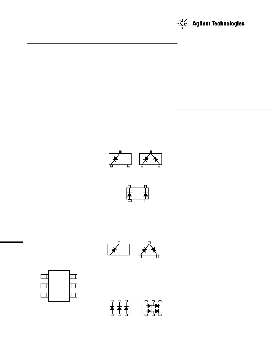
- Lead Code Identification
- Description
- Pin Connections and Package Marking
- DC Electrical Specifications
- RF Electrical Specifications
- Absolute Maximum Ratings
- Equivalent Linear Circuit Model
- SPICE Parameters
- Typical Parameters,Single Diode
- Applications Information
- Assembly Instructions
- SMT Assembly
- Part Number Ordering Information
- Package Dimensions
- Device Orientation
- Tape Dimensions and Product Orientation
Surface Mount Zero Bias
Schottky Detector Diodes
Technical Data
HSMS-285x Series
SOT-23/ SOT-143 Package
Lead Code Identification
(top view)
Description
Agilent's HSMS-285x family of
zero bias Schottky detector
diodes has been designed and
optimized for use in small signal
(P
in
< -20 dBm) applications at
frequencies below 1.5 GHz. They
are ideal for RF/ID and RF Tag
applications where primary (DC
bias) power is not available.
Important Note:
For detector
applications with input power
levels greater than ≠20 dBm, use
the HSMS-282x series at frequen-
cies below 4.0 GHz, and the
HSMS-286x series at frequencies
above 4.0 GHz. The HSMS-285x
series IS NOT RECOMMENDED
for these higher power level
applications.
Available in various package
configurations, these detector
diodes provide low cost solutions
to a wide variety of design prob-
lems. Agilent's manufacturing
techniques assure that when two
diodes are mounted into a single
package, they are taken from
adjacent sites on the wafer,
assuring the highest possible
degree of match.
SOT-323 Package Lead
Code Identification
(top view)
Features
∑ Surface Mount SOT-23/
SOT-143 Packages
∑ Miniature SOT-323 and
SOT-363 Packages
∑ High Detection Sensitivity:
up to 50 mV/
µW at 915 MHz
∑ Low Flicker Noise:
-162 dBV/Hz at 100 Hz
∑ Low FIT (Failure in Time)
Rate*
∑ Tape and Reel Options
Available
∑ Matched Diodes for
Consistent Performance
∑ Better Thermal
Conductivity for Higher
Power Dissipation
∑ Lead-free Option Available
* For more information see the Surface
Mount Schottky Reliability Data Sheet.
SOT-363 Package Lead
Code Identification
(top view)
UNCONNECTED
PAIR
#5
SERIES
#2
SINGLE
#0
1
2
3
1
2
3
4
1
2
3
SERIES
C
SINGLE
B
1
2
3
1
2
3
BRIDGE
QUAD
P
UNCONNECTED
TRIO
L
1
2
3
6
5
4
1
2
3
6
5
4
Pin Connections and
Package Marking
Notes:
1. Package marking provides orienta-
tion and identification.
2. See "Electrical Specifications" for
appropriate package marking.
PLx
1
2
3
6
5
4
2
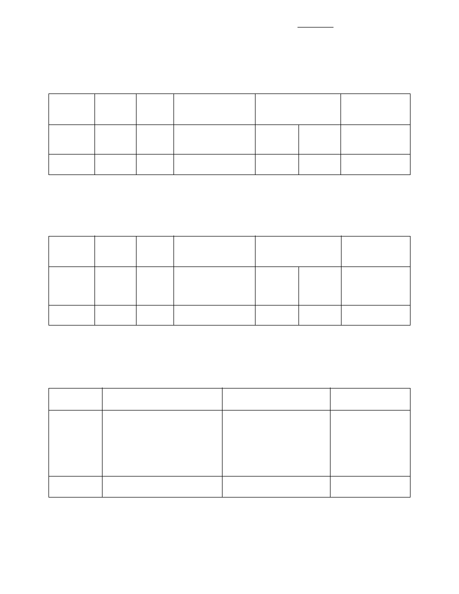
SOT-23/SOT-143 DC Electrical Specifications, T
C
= +25
∞
C, Single Diode
Part
Package
Maximum
Typical
Number
Marking
Lead
Forward Voltage
Capacitance
HSMS-
Code
[1]
Code
Configuration
V
F
(mV)
C
T
(pF)
2850
P0
0
Single
150
250
0.30
2852
P2
2
Series Pair
[2,3]
2855
P5
5
Unconnected Pair
[2,3]
Test
I
F
= 0.1 mA I
F
= 1.0 mA V
R
= ≠0.5 V to ≠1.0V
Conditions
f = 1 MHz
Notes:
1. Package marking code is in white.
2.
V
F
for diodes in pairs is 15.0 mV maximum at 1.0 mA.
3.
C
T
for diodes in pairs is 0.05 pF maximum at ≠0.5 V.
RF Electrical Specifications, T
C
= +25
∞
C, Single Diode
Part Number
Typical Tangential Sensitivity
Typical Voltage Sensitivity
Typical Video
HSMS-
TSS (dBm) @ f = 915 MHz
(mV/
µ
W) @ f = 915 MHz
Resistance RV (K
)
2850
≠ 57
40
8.0
2852
2855
285B
285C
285L
285P
Test
Video Bandwidth = 2 MHz
Power in = ≠40 dBm
Conditions
Zero Bias
R
L
= 100 K
, Zero Bias
Zero Bias
SOT-323/SOT-363 DC Electrical Specifications, T
C
= +25
∞
C, Single Diode
Part
Package
Maximum
Typical
Number
Marking
Lead
Forward Voltage
Capacitance
HSMS-
Code
[1]
Code
Configuration
V
F
(mV)
C
T
(pF)
285B
P0
B
Single
[2]
150
250
0.30
285C
P2
C
Series Pair
[2,3]
285L
PL
L
Unconnected Trio
285P
PP
P
Bridge Quad
Test
I
F
= 0.1 mA I
F
= 1.0 mA
V
R
= 0.5 V to ≠1.0V
Conditions
f = 1 MHz
Notes:
1. Package marking code is laser marked.
2.
V
F
for diodes in pairs is 15.0 mV maximum at 1.0 mA.
3.
C
T
for diodes in pairs is 0.05 pF maximum at ≠0.5 V.
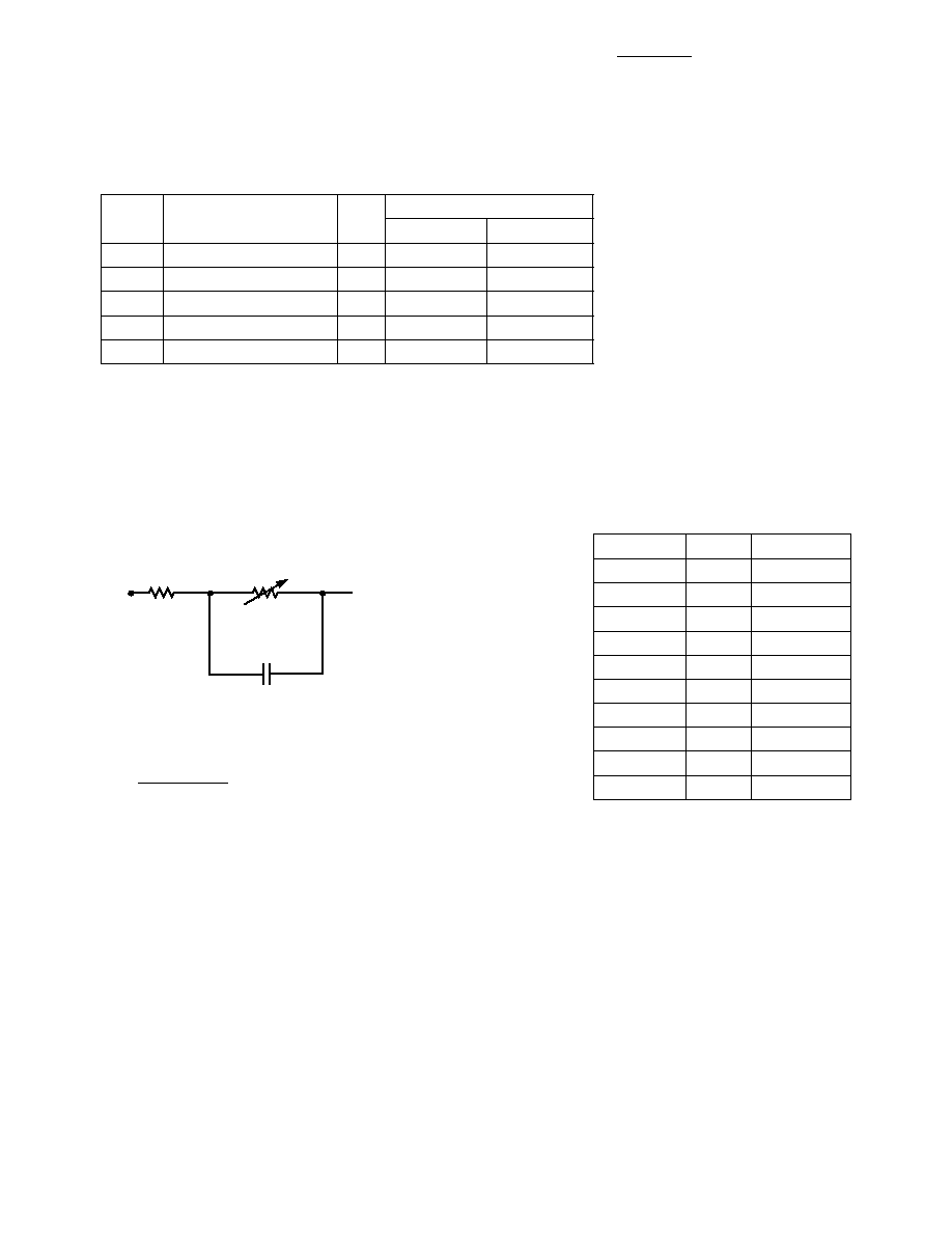
3
Equivalent Linear Circuit Model
HSMS-285x chip
SPICE Parameters
Parameter
Units
HSMS-285x
B
V
V
3.8
C
J0
pF
0.18
E
G
eV
0.69
I
BV
A
3 E -4
I
S
A
3 E-6
N
1.06
R
S
25
P
B
(V
J
)
V
0.35
P
T
(XTI)
2
M
0.5
Absolute Maximum Ratings, T
C
= +25
∞
C, Single Diode
Symbol
Parameter
Unit
Absolute Maximum
[1]
SOT-23/143 SOT-323/363
P
IV
Peak Inverse Voltage
V
2.0
2.0
T
J
Junction Temperature
∞C
150
150
T
STG
Storage Temperature
∞C
-65 to 150
-65 to 150
T
OP
Operating Temperature
∞C
-65 to 150
-65 to 150
jc
Thermal Resistance
[2]
∞C/W
500
150
Notes:
1. Operation in excess of any one of these conditions may result in
permanent damage to the device.
2. T
C
= +25
∞C, where T
C
is defined to be the temperature at the package
pins where contact is made to the circuit board.
ESD WARNING:
Handling Precautions
Should Be Taken To Avoid
Static Discharge.
C
j
R
j
R
S
R
j
=
8.33 X 10
-5
nT
I
b
+ I
s
where
I
b
= externally applied bias current in amps
I
s
= saturation current (see table of SPICE parameters)
T
= temperature,
∞K
n = ideality factor (see table of SPICE parameters)
Note:
To effectively model the packaged HSMS-285x product,
please refer to Application Note AN1124.
R
S
= series resistance (see Table of SPICE parameters)
C
j
= junction capacitance (see Table of SPICE parameters)
4
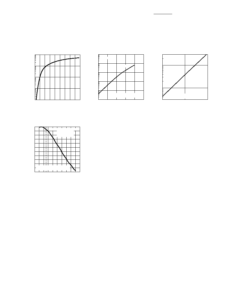
Typical Parameters, Single Diode
Figure 1. Typical Forward Current
vs. Forward Voltage.
Figure 2. +25
∞C Output Voltage vs.
Input Power at Zero Bias.
Figure 3. +25
∞C Expanded Output
Voltage vs. Input Power. See Figure 2.
Figure 4. Output Voltage vs.
Temperature.
I
F
≠ FORWARD CURRENT (mA)
0
0.01
V
F
≠ FORWARD VOLTAGE (V)
0.8 1.0
100
1
0.1
0.2
1.8
10
1.4
0.4 0.6
1.2
1.6
VOLTAGE OUT (mV)
-50
0.1
POWER IN (dBm)
-30
-20
10000
10
1
-40
0
100
-10
1000
R
L
= 100 K
DIODES TESTED IN FIXED-TUNED
FR4 MICROSTRIP CIRCUITS.
915 MHz
VOLTAGE OUT (mV)
-50
0.3
POWER IN (dBm)
-30
10
1
-40
30
R
L
= 100 K
915 MHz
DIODES TESTED IN FIXED-TUNED
FR4 MICROSTRIP CIRCUITS.
OUTPUT VOLTAGE (mV)
0
0.9
TEMPERATURE (
∞C)
40 50
3.1
2.1
1.5
10
100
2.5
80
20 30
70
90
60
1.1
1.3
1.7
1.9
2.3
2.7
2.9
MEASUREMENTS MADE USING A
FR4 MICROSTRIP CIRCUIT.
FREQUENCY = 2.45 GHz
P
IN
= -40 dBm
R
L
= 100 K
5
Applications Information
Introduction
Agilent's HSMS-285x family of
Schottky detector diodes has been
developed specifically for low
cost, high volume designs in small
signal (P
in
< -20 dBm) applica-
tions at frequencies below
1.5 GHz. At higher frequencies,
the DC biased HSMS-286x family
should be considered.
In large signal power or gain con-
trol applications (P
in
> -20 dBm),
the HSMS-282x and HSMS-286x
products should be used. The
HSMS-285x zero bias diode is not
designed for large signal designs.
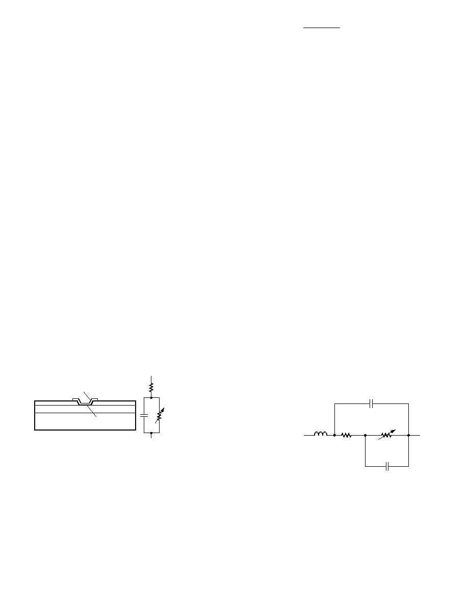
Schottky Barrier Diode
Characteristics
Stripped of its package, a
Schottky barrier diode chip
consists of a metal-semiconductor
barrier formed by deposition of a
metal layer on a semiconductor.
The most common of several
different types, the passivated
diode, is shown in Figure 5, along
with its equivalent circuit.
Figure 5. Schottky Diode Chip.
R
S
is the parasitic series
resistance of the diode, the sum of
the bondwire and leadframe
resistance, the resistance of the
bulk layer of silicon, etc. RF
energy coupled into R
S
is lost as
heat -- it does not contribute to
the rectified output of the diode.
C
J
is parasitic junction capaci-
tance of the diode, controlled by
the thickness of the epitaxial layer
and the diameter of the Schottky
contact. R
j
is the junction
resistance of the diode, a function
of the total current flowing
through it.
8.33 X 10
-5
n T
R
j
= ≠≠≠≠≠≠≠≠≠≠≠≠ = R
V
≠ R
s
I
S
+ I
b
0.026
= ≠≠≠≠≠ at 25
∞C
I
S
+ I
b
where
n = ideality factor (see table of
SPICE parameters)
T = temperature in
∞K
I
S
= saturation current (see
table of SPICE parameters)
I
b
= externally applied bias
current in amps
I
S
is a function of diode barrier
height, and can range from
picoamps for high barrier diodes
to as much as 5
µA for very low
barrier diodes.
The Height of the Schottky
Barrier
The current-voltage characteristic
of a Schottky barrier diode at
room temperature is described by
the following equation:
V - IR
S
I = I
S
(exp
(
≠≠≠≠≠≠
)
- 1)
0.026
On a semi-log plot (as shown in
the Agilent catalog) the current
graph will be a straight line with
inverse slope 2.3 X 0.026 = 0.060
volts per cycle (until the effect of
R
S
is seen in a curve that droops
at high current). All Schottky
diode curves have the same slope,
but not necessarily the same value
of current for a given voltage. This
is determined by the saturation
current, I
S
, and is related to the
barrier height of the diode.
Through the choice of p-type or
n-type silicon, and the selection of
metal, one can tailor the charac-
teristics of a Schottky diode.
Barrier height will be altered, and
at the same time C
J
and R
S
will be
changed. In general, very low
barrier height diodes (with high
values of I
S
, suitable for zero bias
applications) are realized on
p-type silicon. Such diodes suffer
from higher values of R
S
than do
the n-type. Thus, p-type diodes are
generally reserved for small signal
detector applications (where very
high values of R
V
swamp out high
R
S
) and n-type diodes are used for
mixer applications (where high
L.O. drive levels keep R
V
low).
Measuring Diode Parameters
The measurement of the five
elements which make up the low
frequency equivalent circuit for a
packaged Schottky diode (see
Figure 6) is a complex task.
Various techniques are used for
each element. The task begins
with the elements of the diode
chip itself.
L
P
R
S
R
V
C
j
C
P
FOR THE HSMS-285x SERIES
C
P
= 0.08 pF
L
P
= 2 nH
C
j
= 0.18 pF
R
S
= 25
R
V
= 9 K
Figure 6. Equivalent Circuit of a
Schottky Diode.
R
S
R
j
C
j
;;
METAL
SCHOTTKY JUNCTION
PASSIVATION
PASSIVATION
N-TYPE OR P-TYPE EPI LAYER
N-TYPE OR P-TYPE SILICON SUBSTRATE
CROSS-SECTION OF SCHOTTKY
BARRIER DIODE CHIP
EQUIVALENT
CIRCUIT