Document Outline
- List of Figures
- 1. Conversion Gain, IF P 1 dB. . .
- 2. Conversion Gain, IF P 1 dB. . .
- 3. Typical RF to IF Conversion Gain vs. RF Frequency. . .
- 4. RF, LO and IF Port VSWR vs. Frequency.
- 5. RF to IF Conversion Gain vs. LO Power.
- 6. RF to IF Conversion Gain vs. IF Frequency.
- 7. RF Feedthrough Relative to IF Carrier, dBm LO to RF and IF Leakage vs. Frequency.
- 8. Harmonic Intermodulation Suppression. . .
- Features
- Description
- Typical Biasing Configuration and Functional Block Diagram
- Plastic SO-8 Package
- Pin Configuration
- IAM-81008 Absolute Maximum Ratings
- IAM-81008 Part Number Ordering Information
- IAM-81008 Electrical Specifications [1] , TA = 25∞C
- IAM-81008 Typical Performance, T A = 25∞C, V CC = 5 V. . .
- Package Dimensions

7-119
Silicon Bipolar MMIC 5 GHz
Active Double Balanced
Mixer/IF Amp
Technical Data
Features
∑ RF-IF Conversion Gain
From 0.05≠ 5 GHz
∑ IF Conversion Gain From
DC to 1 GHz
∑ Low Power Dissipation:
65 mW at V
CC
= 5 V Typical
∑ Single Polarity Bias Supply:
V
CC
= 4 to 8 V
∑ Load-insensitive Performance
∑ Conversion Gain Flat Over
Temperature
∑ Low LO Power Requirements:
≠5 dBm Typical
∑ Low Cost Plastic Surface
Mount Package
IAM-81008
Plastic SO-8 Package
Pin Configuration
Description
The IAM-81008 is a complete low
power consumption, double
balanced active mixer housed in a
miniature low cost plastic surface
mount package. It is designed for
narrow or wide bandwidth commer-
cial and industrial applications
having RF inputs up to 5 GHz.
Operation at RF and LO frequencies
less than 50 MHz can be achieved
using optional external capacitors
to ground. The IAM-81008 is
particularly well suited for applica-
tions that require load-insensitive
conversion and good spurious
signal suppression with minimum
LO and bias power consumption.
Typical applications include
frequency down conversion,
modulation, demodulation and
phase detection. Markets include
fiber-optics, GPS satelite navigation,
mobile radio, and battery powered
communications receivers.
The IAM series of Gilbert multiplier-
based frequency converters is
fabricated using HP's 10 GHz, f
T
,
25 GHz f
MAX
ISOSATTM-I silicon
bipolar process. This process uses
nitride self alignment,
submicrometer lithography, trench
isolation, ion implantation, gold
metallization and polyimide inter-
metal dielectric and scratch protec-
tion to achieve excellent perfor-
mance, uniformity and reliability.
C
block
C
block
C
block
C
block
V
CC
= 5 V
V
ee
= 0 V
LO Input
RF Input
IF Output
1
2
3
4
Note: No external baluns are required.
Optional Low
Frequencies
RF Ground
Optional Low
LO Ground
8
7
6
5
Typical Biasing Configuration and
Functional Block Diagram
POWER CONTROL
RF
IN
V
CC1
GROUND AND
THERMAL
CONTACT
GROUND AND
THERMAL
CONTACT
1
8
2
7
RF
OUT
AND V
CC2
GROUND
3
6
4
5
5965-9107E
7-120
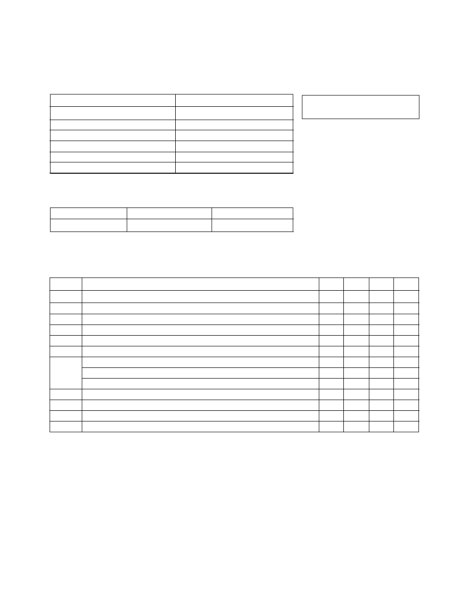
IAM-81008 Absolute Maximum Ratings
Parameter
Absolute Maximum
[1]
Device Voltage
10 V
Power Dissipation
2,3
300 mW
RF Input Power
+14 dBm
LO Input Power
+14 dBm
Junction Temperature
150
∞
C
Storage Temperature
≠65 to 150
∞
C
Thermal Resistance:
jc
= 80
∞
C/W
Notes:
1. Permanent damage may occur if
any of these limits are exceeded.
2. T
CASE
= 25
∞
C.
3. Derate at 4.4 mW/
∞
C for T
C
> 82
∞
C.
IAM-81008 Part Number Ordering Information
Part Number
Devices Per Reel
Reel Size
IAM-81008-TR1
1000
7"
For more information, see "Tape and Reel Packaging for Semmiconductor Devices".
IAM-81008 Electrical Specifications
[1]
, T
A
= 25
∞
C
Symbol
Parameters and Test Conditions: V
cc
= 5 V, Z
O
= 50
, LO =≠5 dBm, RF = ≠20 dBm
Units
Min.
Typ.
Max.
G
C
Conversion Gain
RF = 2 GHz, LO = 1.75 GHz
dB
6.0
8.5
10
F
3 dB
RF
RF Bandwidth (G
C
3 dB Down)
IF = 250 MHz
GHz
3.5
F
3 dB
IF
IF Bandwidth (G
C
3 dB Down)
LO = 2 GHz
GHz
0.6
P
1 dB
IF Output Power at 1 dB Gain Compression
RF = 2 GHz, LO = 1.75 GHz
dBm
≠6
IP
3
IF Output Third Order Intercept Point
RF = 2 GHz, LO = 1.75 GHz
dBm
3
NF
SSB Noise Figure
RF = 2 GHz, LO = 1.75 GHz
dB
17
RF Port VSWR
f = 0.05 to 3.5 GHz
1.5:1
VSWR
LO Port VSWR
f = 0.05 to 3.5 GHz
2.0:1
IF Port VSWR
f < 1 GHz
1.5:1
RF
if
RF Feedthrough at IF Port
RF = 2 GHz, LO = 1.75 GHz
dBc
≠25
LO
if
LO Leakage at IF Port
LO = 1.75 GHz
dBm
≠25
LO
rf
LO Leakage at RF Port
LO = 1.75 GHz
dBm
≠30
I
CC
Supply Current
mA
10
13
16
Note:
1. The recommended operating voltage range for this device is 4 to 8 V. Typical performance as a function of voltage is on
the following page.

7-121
IAM-81008 Typical Performance, T
A
= 25
∞
C, V
CC
= 5 V
RF: ≠20 dBm at 2 GHz, LO: ≠5 dBm at 1.75 GHz
(unless otherwise noted)
≠10
≠5
0
5
0
0
2
4
6
8
10
10
20
30
IF P
1 dB
(dBm)
0
5
10
15
G
C
(dB)
I
CC
(mA)
V
CC
(V)
Figure 1. Conversion Gain, IF P
1 dB
and I
CC
Current vs. V
CC
Bias Voltage.
I
CC
G
C
P
1 dB
≠10
≠5
0
5
5
≠55
≠25
+25
+85
+125
10
15
20
IF P
1 dB
(dBm)
0
5
10
15
G
C
(dB)
I
CC
(mA)
TEMPERATURE (∞C)
Figure 2. Conversion Gain, IF P
1 dB
and I
CC
Current vs. Case Temperature.
G
C
P
1 dB
I
CC
≠5
0
5
10
G
C
(dB)
0.1
0.2
0.5
1.0
2.0
5.0
10
RF FREQUENCY (GHz)
Figure 3. Typical RF to IF Conversion
Gain vs. RF Frequency, T
A
= 25∞C
(Low Side LO).
1:1
2:1
3:1
4:1
VSWR
0.1
1.0
10
FREQUENCY (GHz)
Figure 4. RF, LO and IF Port VSWR
vs. Frequency.
0
2
4
6
8
10
G
C
(dB)
≠15
≠5
0
≠10
5
LO POWER (dBm)
Figure 5. RF to IF Conversion Gain
vs. LO Power.
IF = 70 MHz
IF = 1 GHz
RF
LO
IF
≠40
≠30
≠20
≠10
0
RF to IF (dBc)
LO to RF and IF (dBm)
0.1
1.0
10
FREQUENCY (GHz)
Figure 7. RF Feedthrough Relative to
IF Carrier, dBm LO to RF and IF
Leakage vs. Frequency.
0.01
0.1
1.0
2.0
FREQUENCY, RF≠LO (GHz)
Figure 6. RF to IF Conversion Gain
vs. IF Frequency.
≠2
0
2
4
6
8
10
G
C
(dB)
0
1
2
3
4
5
HARMONIC RF ORDER
Xmn = Pif ≠ P(m*rf ≠ n*lo)
Figure 8. Harmonic Intermodulation
Suppression (dB Below Desired Output)
RF at 1 GHz, LO at 0.752 GHz, IF at 0.248 GHz.
--
18
16
42
29
45
21
0
35
20
44
36
35
45
42
44
52
57
74
48
72
59
64
64
>75
>75
>75
>75
>75
>75
>75
>75
>75
>75
>75
>75
0
1
2
3
4
5
HARMONIC LO ORDER
LO = 2 GHz
High Side LO
Low Side LO
RF to IF
LO to IF
LO to RF
7-122
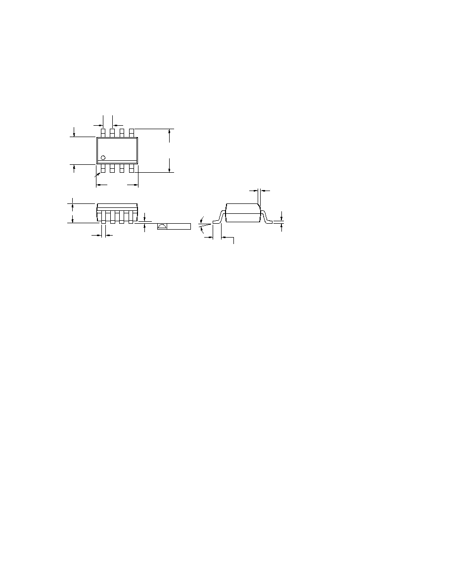
Package Dimensions
SO-8 Plastic Package
5.84/6.20
(.230/.244)
3.80/4.00
(.1497/.1574)
Pin 1
1.27 (.050)
6x
4.72/5.00
(.186/.197)
0.10/0.25
(.004/.0098)
0.33/0.51
(.013/.020) 8X
1.35/1.75
(.0532/.0688)
0.19/0.25
(.0075/.0098)
0.41/1.27
(.016/.050)
0
∞
/8
∞
0.38
±
0.10
(.015
±
.004) x 45
∞
0.10 (.004)
Note:
1. Dimensions are shown in millimeters (inches).
M810