 | –≠–ª–µ–∫—Ç—Ä–æ–Ω–Ω—ã–π –∫–æ–º–ø–æ–Ω–µ–Ω—Ç: IAM-82028 | –°–∫–∞—á–∞—Ç—å:  PDF PDF  ZIP ZIP |
Document Outline
- List of Figures
- 1. Conversion Gain, IF P1 dB and Icc Curren vs. Vcc Bias voltage.t
- 2. Conversion Gain, IF P 1 dB and Icc Current vs. Case Temperature.
- 3. Typical RF to IF Conversion Gain vs. RF Frequency. . .
- 4. RF, LO and IF Port VSWR vs. Frequency.
- 5. RF to IF Conversion Gain vs. LO Power.
- 6. RF to IF Conversion Gain vs. IF Frequency.
- 7. RF Feedthrough Relative to IF Carrier, dBm LO to RF and IF Leakage vs. Frequency.
- 8. Harmonic Intermodulation Suppression. . .
- Features
- Typical Biasing Configuration and Functional Block Diagram
- Description
- 28 Package
- Absolute Maximum Ratings
- IAM-82028 Electrical Specifications [1] , TA = 25∞C
- Typical Performance, T A = 25∞C, V CC = 10 V. . .
- Package Dimensions

7-131
IAM-82028
Silicon Bipolar MMIC 5 GHz
Active Double Balanced Mixer/
IF Amp
Technical Data
5965-9114E
Features
∑
15 dB RF-IF Conversion
Gain from 0.05 - 5 GHz
∑ IF Output from DC to 2 GHz
∑ IF Output P
ldB
up to
+12 dBm
∑ Single Polarity Bias Supply:
V
CC
= 7 to 13 V
∑ Load-Insensitive
Performance
∑ Conversion Gain Flat Over
Temperature
∑ Low LO Power Requirements:
0 dBm Typical
∑ Low RF to IF Feedthrough,
Low LO Leakage
∑ Hermetic Ceramic Surface
Mount Package
Description
The IAM-82028 is a complete
moderate-power double-balanced
active mixer housed in a
miniature ceramic hermetic
surface mount package. It is
designed for narrow or wide
bandwidth commercial, industrial
and military applications having
RF inputs up to 5 GHz and IF
outputs from DC to 2 GHz.
Operation at RF and LO
frequencies less than 50 MHz can
be achieved using optional
external capacitors to ground.
The IAM-82028 is particularly well
suited for applications that
require load-insensitive
conversion gain and good
spurious signal suppression and
moderate dynamic range with
minimum LO power. Typical
applications include frequency
downconversion, modulation,
demodulation and phase
detection for fiber-optic, GPS
satellite navigation, mobile radio,
and communications receivers.
The IAM series of Gilbert
multiplier-based frequency
converters is fabricated using
HP's 10 GHz f
T
, 25 GHz f
MAX
ISOSAT
TM
-I silicon bipolar process
which uses nitride self-alignment,
submicrometer lithography,
trench isolation, ion implantation,
gold metallization and polyimide
inter-metal dielectric and scratch
protection to achieve excellent
performance, uniformity and
reliability.
28 Package
Typical Biasing Configuration and
Functional Block Diagram
PIN 1

7-132
Absolute Maximum Ratings
Absolute
Parameter
Maximum
[1]
Device Voltage
15 V
Power Dissipation
[2,3]
1200 mW
RF Input Power
+14 dBm
LO Input Power
+14 dBm
Junction Temperature
200
∞
C
Storage Temperature
-65
∞
C to 200
∞
C
Thermal Resistance:
[2,4]
jc
= 45
∞
C/W
Notes:
1. Permanent damage may occur if any of
these limits are exceeded.
2. T
CASE
= 25
∞
C.
3. Derate at 22.2 mW/
∞
C for T
C
>146
∞
C.
4. See MEASUREMENTS section
"'Thermal Resistance" in
Communications Components Catalog,
for more information.
IAM-82028 Electrical Specifications
[1]
,
T
A
= 25
∞
C
Parameters and Test Conditions
[2]
:
Symbol
V
CC
= 10 V, V
ee
= 0 V, V
gc
= 0 V, Z
O
= 50
Units
Min.
Typ.
Max.
G
C
Conversion Gain
RF = 2 GHz, LO = 1.75 GHz
dB
13.5
15
16.5
f
3dB
RF
RF Bandwidth
IF = 250 MHzz
GHz
5.5
(G
C
3 dB Down)
f
3dB
IF
IF Bandwidth
LO = 2 GH
GHz
0.6
(G
C
3 dB Down)
P
1dB
IF Output Power at
RF = 2 GHz, LO = 1.75 GHz
dBm
8
1 dB Gain Compression
IP
3
IF Output Third
RF = 2 GHz, LO = 1.75 GHz
dBm
18
Order Intercept Point
NF
SSB Noise Figure
RF = 2 GHz, LO = 1.75 GHz
dB
16
VSWR
RF Port VSWR
f = 0.05 to 5 GHz
1.5:1
LO Port VSWR
f = 0.05 to 5 GHz
2:1
IF Port VSWR
f < 2 GHz
2.3:1
RF
if
RF Feedthrough at IF Port
RF = 2 GHz, LO = 1.75 GHz
dBc
-30
LO
if
LO Leakage at IF Port
LO = 1.75 GHz
dBm
-20
LO
rf
LO Leakage at RF Port
LO = 1.75 GHz
dBm
-30
I
CC
Supply Current
mA
40
55
65
Note:
1. The recommended operating voltage range for this device is 7 to 13 V. Typical performance as a function of voltage is on the following
page.
7-133
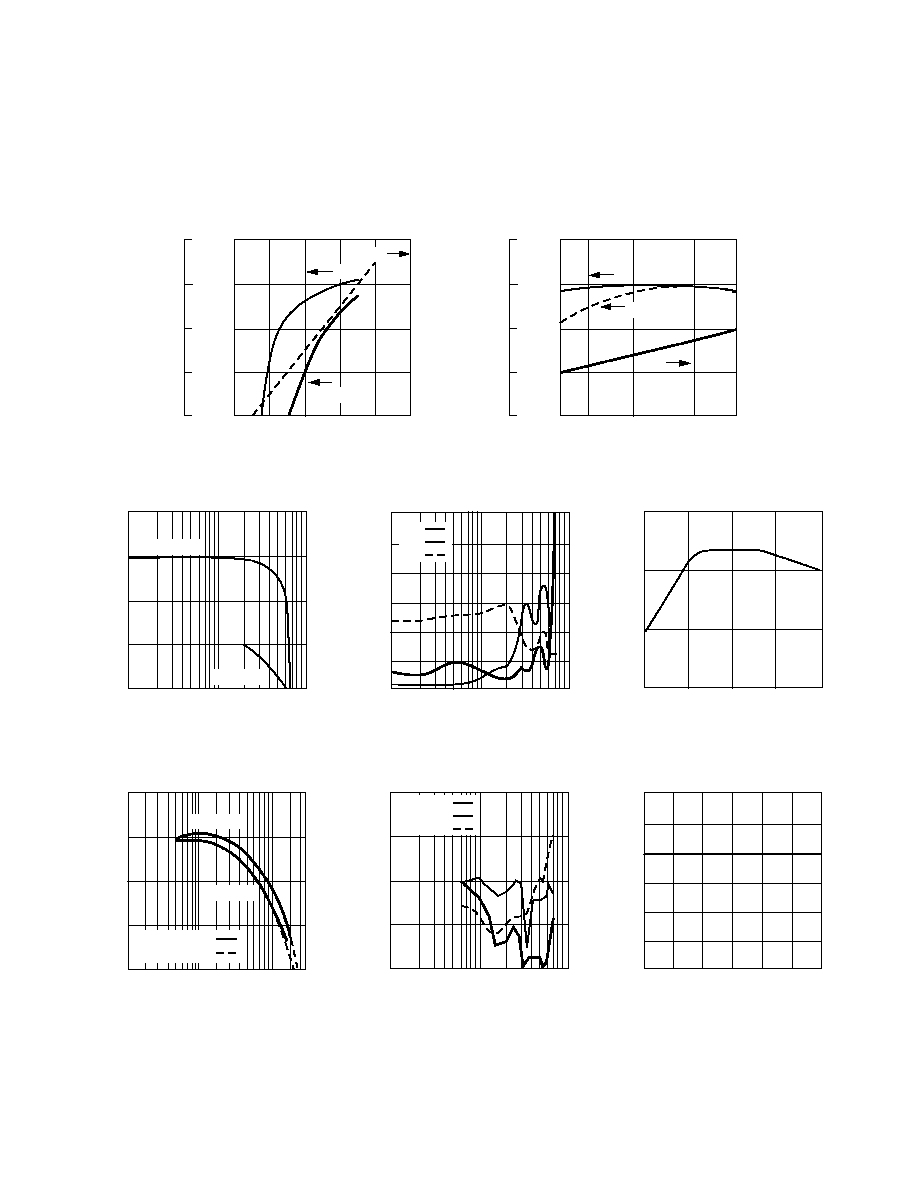
Typical Performance, T
A
= 25
∞
C, V
CC
= 10 V
RF: -20 dBm at 2 GHz, LO: 0 dBm at 1.75 GHz
(unless otherwise noted)
0
5
10
15
20
0
0
4
8
12
16
20
50
25
75
100
IF P
1 dB
(dBm)
0
5
10
15
20
G
C
(dB)
I
CC
(mA)
V
CC
(V)
Figure 1. Conversion Gain, IF P
1 dB
and I
CC
Current vs. V
CC
Bias Voltage.
I
CC
G
C
P
1 dB
0
5
10
15
20
≠5
15
40
≠55
≠25
+25
+85
+125
50
70
60
80
IF P
1 dB
(dBm)
G
C
(dB)
I
CC
(mA)
TEMPERATURE (
∞
C)
Figure 2. Conversion Gain, IF P
1 dB
and I
CC
Current vs. Case Temperature.
G
C
P
1 dB
I
CC
0
5
15
10
20
G
C
(dB)
0.1
0.2
0.5
1.0
2.0
5.0
10
RF FREQUENCY (GHz)
Figure 3. Typical RF to IF Conversion
Gain vs. RF Frequency, T
A
= 25
∞
C
(Low Side LO).
1:1
2:1
3:1
4:1
VSWR
0.1
1.0
10
FREQUENCY (GHz)
Figure 4. RF, LO and IF Port VSWR
vs. Frequency.
10
12
14
16
G
C
(dB)
≠10
0
5
≠5
10
LO POWER (dBm)
Figure 5. RF to IF Conversion Gain
vs. LO Power.
IF = 70 MHz
IF = 1 GHz
RF
LO
IF
≠40
≠30
≠20
≠10
0
RF to IF (dBc)
LO to RF and IF (dBm)
0.1
1.0
10
FREQUENCY (GHz)
Figure 7. RF Feedthrough Relative to
IF Carrier, dBm LO to RF and IF
Leakage vs. Frequency.
0.01
0.1
1.0
4.0
2.0
FREQUENCY, RF≠LO (GHz)
Figure 6. RF to IF Conversion Gain
vs. IF Frequency.
0
5
10
15
20
G
C
(dB)
0
1
2
3
4
5
HARMONIC RF ORDER
Xmn = Pif ≠ P(m*rf ≠ n*lo)
Figure 8. Harmonic Intermodulation
Suppression (dB Below Desired Output)
RF at 1 GHz, LO at 0.752 GHz, IF at 0.248 GHz.
--
12
6
27
22
41
23
0
35
18
38
36
40
52
43
59
52
73
>75
60
>75
74
>75
74
>75
>75
>75
>75
>75
>75
>75
>75
>75
>75
>75
>75
0
1
2
3
4
5
HARMONIC LO ORDER
High Side LO
Low Side LO
RF to IF
LO to IF
LO to RF
0
5
10
LO = 2 GHz
LO = 4 GHz
High Side LO
Low Side LO

7-134
4.57
±
0.13
(0.180
±
0.005 SQ)
5.33
±
0.25
(0.210
±
0.010)
2.54
±
0.25
(0.100
±
0.010)
10.16
±
0.25
(0.400
±
0.010)
END VIEW
TOP VIEW
0.13
±
0.05
(0.005
±
0.002)
8
∞
MAX.
1.78
±
0.25
(0.070
±
0.010)
0.76
±
0.13
(0.030
±
0.005)
0.08
±
0.08
(0.003
±
0.003)
0.38
±
0.08
(0.015
±
0.003)
1.27 (0.050) TYP.
1
2
3
4
8
7
6
5
2.08
±
0.25
(0.082
±
0.010)
SIDE VIEW
DIMENSIONS ARE IN MILLIMETERS (INCHES)
M820
Package Dimensions
28 Package