 | –≠–ª–µ–∫—Ç—Ä–æ–Ω–Ω—ã–π –∫–æ–º–ø–æ–Ω–µ–Ω—Ç: 1653 | –°–∫–∞—á–∞—Ç—å:  PDF PDF  ZIP ZIP |
AIC1653
Micropower Inverting DC/DC Converter in SOT-23-5
Analog Integrations Corporation
4F, 9 Industry E. 9th Rd, Science-Based Industrial Park, Hsinchu, Taiwan
DS-1653-02 122203
TEL: 886-3-5772500
FAX: 886-3-5772510
www.analog.com.tw
1
FEATURES
Low Quiescent Current:
15
µA in Active Mode
<1
µA in Shutdown Mode
Operates with VIN as Low as 1.8V
Uses Small Surface Mount Components
High Output Voltage: Up to -28V
Low profile 5-Lead SOT-23-5 Package
APPLICATIONS
LCD Bias
Hand-Held Computers
Battery Backup
Digital Still Cameras
DESCRIPTION
The AIC1653 is a micropower inverting DC/DC
converter in 5-lead SOT-23 package. It is designed
for power systems with a 100mA current limit and
an input voltage ranging from 1.8V to 10V. Besides,
AIC1653 features a quiescent current of only 15
µA
at no load, which further reduces to 0.5µA when
shutdown. The schemes of current limited and
fixed off-time control conserve operating current,
resulting in high efficiency over a broad range of
load current. In addition, the 30V switch of
AIC1653 allows high voltage outputs up to -28V,
which is easily generated without the use of costly
transformers. The AIC1653's low off-time of 400ns
permits the use of tiny, low profile inductors and
capacitors to minimize footprint and cost in
space-conscious portable applications.
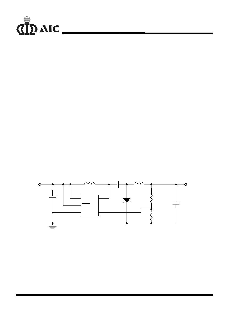
TYPICAL APPLICATION CIRCUIT
L1
22
µH
C3
0.22
µF
L2
22
µH
D1
C1
4.7
µF
V
IN
2.5V~5V
R1
150k
R2
39K
C2
4.7
µF
V
OUT
-6V/14mA
VIN
5
SHDN
4
GND
2
SW
1
NFB 3
AIC1653
RB521S-30
L1,L2: TOKO D312F 22
µH
D1: Rohm RB521S-30
C1,C2,C3: TAIYO YUDEN Ceramic capacitors

AIC1653
ORDERING INFORMATION
AIC1653CXXX
Example: AIC1653CVTR
in SOT-23-5 Package & Tape & Reel
Packing Type
PIN CONFIGURATION
SOT-23-5 (CV)
FRONT VIEW
1: SW
2: GND
3: NFB
4. SHDN
5: VIN
3
2
1
4
5
PACKING TYPE
TR: TAPE & REEL
BG: BAG
PACKAGE TYPE
V: SOT-23-5
SOT-23-5 Marking
Part No.
Marking
AIC1653 1653
ABSOLUTE MAXIMUM RATINGS
(Note 1)
VIN, SHDN Voltage
10V
SW Voltage
30V
NFB Voltage
-3V
Junction Temperature
125∞C
Operating Temperature Range (Note 2)
-40∞C to 85∞C
Storage Temperature Range
-65
∞C to 150∞C
Lead Temperature (Soldering, 10 sec)
300∞C
TEST CIRCUIT
Refer to Typical Application Circuit.
2
AIC1653
ELECTRICAL CHARACTERISTICS
(T
A
= 25∞C, V
IN
= 3.6V, V
SHDN
= 3.6V unless
otherwise specified)
PARAMETER
TEST CONDITIONS
MIN.
TYP. MAX.
UNIT
Minimum Input Voltage
1.8
V
Not Switching
15
20
Quiescent Current
V
SHDN
= 0V
1
µA
FB Comparator Trip Point
-1.205 -1.23 -1.255
V
FB Comparator Hysteresis
10
mV
Output Voltage Line Regulation (Note
3)
Refer to Fig.7
0.05
%/V
FB Pin Bias Current (Note 4)
V
NFB
= ≠1.23V
1.3
2
2.7
µA
NFB
-1V
400
nS
Switch Off Time
NFB
-0.6V
800
nS
Inter Switch On-Resistance
0.6
1
1.4
Switch Current Limit
75
100
125
mA
SHDN
Input Voltage High
0.9
V
SHDN
Input Voltage Low
0.25
V
Switch Leakage Current
Switch Off, V
SW
= 5V
0.01
5
µA
Note 1: Absolute Maximum Ratings are those values beyond which the life of a device may be impaired.
Note 2: Specifications over the -40∞C to 85∞C operating temperature range are assured by design,
characterization and correlation with statistical process controls.
Note 3: Output voltage line regulation is guaranteed by design, characterization and correlation with
statistical quality controls, not production tested.
Note 4: Bias current flows out of the NFB pin.
3
AIC1653
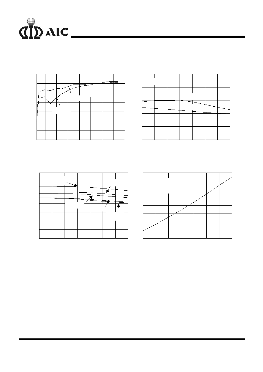
TYPICAL PERFORMANCE CHARACTERISTICS
Fig. 1 Load Current vs. Efficiency
(Refer to typical application circuit)
E
f
f
i
ci
e
n
cy (
%
)
Load Current (mA)
2
4
6
8
10
12
14
16
45
50
55
60
65
70
75
80
V
IN
=4.2V
V
IN
=2.7V
Fig. 2 FB Comparator Trip Point and Pin Bias
Current vs. Temperature
FB Comp
ar
ator T
r
ip
Poi
n
t (V)
Temperature (
∞C)
-40
-20
0
20
40
60
80
100
-1.20
-1.21
-1.22
-1.23
-1.24
-1.25
Current
Voltage
V
IN
=3.6V
0
1
2
3
4
5
B
i
a
s
Cu
rre
n
t
(
µ
A)
-40
-20
0
20
40
60
80
100
0
20
40
60
80
100
120
140
V
IN
=10V
V
IN
=8.5V
V
IN
=4.2V
V
IN
=3.6V
V
IN
=2.5V
Fig. 3 Switch Current Limit vs. Temperature
Switch Cur
r
ent
Lim
i
t (mA)
Temperature (
∞C)
-40
-20
0
20
40
60
80
100
0.7
0.8
0.9
1.0
1.1
1.2
1.3
1.4
1.5
V
IN
=3.6V,
I
SWITCH
=50mA
Fig. 4 Switch ON-Resistance vs. Temperature
Sw
it
ch O
N
-Resistance
(
)
Temperature (
∞C)
4

AIC1653
TYPICAL PERFORMANCE CHARACTERISTICS
(Continued)
Fig. 5 Switch Off Time vs. Temperature
S
w
i
t
ch Off Ti
me
(
ns
)
Temperature (
∞C)
-40
-
20
0
20
40
60
80
100
400
450
500
550
600
650
700
750
800
850
Phase II
Phase I
V
IN
=3.6V
Fig. 6 Quiescent Current vs. Temperature and Voltage
S
u
p
p
l
y
C
u
rren
t
(u
A
)
Supply Voltage (V)
2
4
6
8
10
12
10
12
14
16
18
20
22
24
-40
-20
0
20
40
60
80
100
Temperature=-40
∞C to 100∞C,
V
IN
=3.6V
V
IN
=1.8V to 12V,
Temperature = 20
∞C
Temperature (
∞C)
Fig. 7 Line Regulation
O
u
tput
Voltage
(V
)
Input Voltage (V)
2
3
4
5
6
7
8
9
10
5.0
5.2
5.4
5.6
5.8
6.0
6.2
6.4
6.6
6.8
7.0
V
OUT
= - 6.0V,
I
OUT
=2mA
5