AIC1086
1.5A Low Dropout Positive Adjustable Regulator
Analog Integrations Corporation 4F, 9, Industry E. 9th Rd, Science Based Industrial Park, Hsinchu Taiwan, ROC
www.analog.com.tw
DS-1086-00 May 16, 00
TEL: 886-3-5772500 FAX: 886-3-5772510
1
n
FEATURES
l
Dropout Voltage 1.3V at 1.5A Output Current.
l
Fast Transient Response.
l
Line Regulation typically at 0.015%.
l
Load Regulation typically at 0.1%.
l
Internal Thermal and Current Limiting.
l
Adjustable Output Voltage or Fixed 2.85V, 3.3V,
5V.
l
Standard 3-Pin Power Packages.
n
APPLICATIONS
l
Post Regulator for Switching Supply.
l
Battery Chargers.
l
Constant-Current Regulators.
l
PC Add-On Card.
n
DESCRIPTION
The AIC1086 is a low dropout three terminal
regulator with 1.5A output current capability. The
output voltage is adjustable with the use of a
resistor divider or fixed 2.85V, 3.3V, 5V. Dropout
is guaranteed at a maximum of 1.5V at
maximum output current. Its low dropout voltage
and fast transient response make it ideal for low
voltage microprocessor applications. Internal
current and thermal limiting provides protection
against any overload condition that would create
excessive junction temperatures.
n
TYPICAL APPLICATION CIRCUIT
C2
10
µ
F
V
OUT
3.3V
V
IN
5V
+
+
V
REF
RF2
205
1%
ADJ
AIC1086
C1
10
µ
F
2
3
1
RF1
125
1%
V
REF
=V
OUT
- V
ADJ
=1.25V (typ.)
V
OUT
=V
REF
x (1+RF2/RF1)+ I
ADJ
x RF2
I
ADJ
=55
µ
A (typ.)
(1) C1 needed if device is far away from filter
capacitors.
(2) C2 required for stability.
Adjustable Voltage Regulator
C2
10
µ
F
V
OUT
3.3V
V
IN
5V
+
+
GND
C1
10
µ
F
AIC1086-33
Fixed Voltage Regulator
AIC1086
2
n
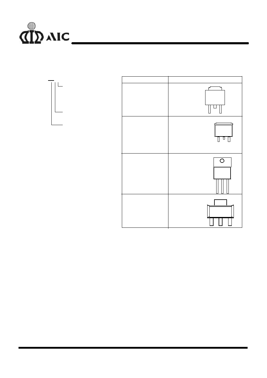
ORDERING INFORMATION
ORDER NUMBER
PIN CONFIGURATION
AIC1 086-XXXX
PACKAGING TYPE
E: TO-252
M: TO-263
T: TO-220
Y: SOT-223
TEMPERATURE RANGE
C: 0
∞
C~+70
∞
C
DEFAULT:ADJ.
28: 2.85V
33: 3.3V
50: 5.0V
FRONT VIEW
1: ADJ
2: VOUT (TAB)
3: VIN
AIC1086CM
(TO-2 63)
1
2
3
FRONT VIEW
1: ADJ
2: VOUT (TAB)
3: VIN
FRONT VIEW
1: ADJ
2: VOUT (TAB)
3: VIN
AIC1086 CT
(TO-220)
AIC1086 CY
(SOT-223)
2
3
1
2
3
1
FRONT VIEW
1: ADJ
2: VOUT (TAB)
3: VIN
AIC1086CE
(TO-252)
2
3
1
n
ABSOLUTE MAXIMUM RATINS
VIN pin to ADJ/GND pin .............................. ... .......... ... .......... ... ... ... ... ...................... 7V
Operating Junction Temperature Range
..................... ... ... ...................... 0
∞
C ~ 125
∞
C
Storage Temperature Range
.................................. ... ... ... ................. - 65
∞
C ~ 150
∞
C
Thermal Resistance (Junction to Case)
TO-220 ... ... ... ........... ... ...... ... ... ... ... 3
∞
C /W
TO-263 ... ....... ... ....... ... ... ... ... ... ... ... . 3
∞
C /W
SOT-223
... ....... ... ..... ... ... ..... ... ... ..15
∞
C /W
Lead Temperature (Soldering) 10 sec.
........................ ... ... ............... ... ... ...... .......260
∞
C

AIC1086
4
n
TYPICAL PERFORMANCE CHARACTERISTICS
Load Current
Load Transient Response
Time (
µ
S)
0
40
80
120
160
200
0.1A
0.4A
-0.1
-0.05
0
0.05
0.1
Output Voltage
(V, AC)
V
IN
=5V
C
IN
=1
µ
F
C
OUT
=10
µ
F (Tantalum)
V
OUT
=3.3V
Line Transient Response
Time (
µ
S)
Output Voltage
(
mV, AC)
Input Voltage (V)
0
10
20
30
40
50
6.0
7.0
--100
--50
0
50
C
OUT
=10
µ
F (Tantalum)
V
OUT
=3.3V
0
200
400
600
800
1000
1200
1400 1600
1.18
1.20
1.22
1.24
1.26
1.28
1.30
Dropout Voltage (V
OUT
=3.3V)
Minimum Differential Voltage (V)
Output Current (mA)
Minimum Operating Current
Differential Voltage (V)
Minimum Operating Current (
mA)
0
1
2
3
4
5
0.2
0.4
0.6
0.8
1.0
1.2
1.4
1.6
1.8