AIC1383B
3A Termination Regulator
Analog Integrations Corporation
Si-Soft Research Center
DS-1383BP-03 010405
3A1, No.1, Li-Hsin Rd. I, Science Park, Hsinchu 300, Taiwan, R.O.C.
FEATURES
3A Source and Sink Current Ability
Support DDR1 (1.25V
TT
) and DDR2 (0.9V
TT
)
Requirements
Low Output Voltage Offset,
�20mV
High Accuracy Output Voltage at Full-Load
Adjustable V
OUT
by External Resistor
Low External Component Count
Current Limit protection
Thermal Protection
SOP-8, TO-252 and TO-263 Packages
APPLICATIONS
Mother Board
Graphic Cards
DDR Termination Voltage Supply
DESCRIPTION
AIC1383B linear regulator is designed to
achieve 3A source and sink current while
regulating an output voltage to within 45mV.
AIC1383B converts voltage supplies range
from 1.6V to 6V into an output voltage that
adjusts by two external voltage divider
resistors. It provides an excellent voltage
source for active termination schemes of high-
speed transmission lines as those seen in
high-speed memory buses, and it meets the
JEDEC SSTL-2 and SSTL-3 specifications for
termination of DDR-SRAM.
Built-in current limiting in source and sink
mode, with thermal shutdown provide
maximal protection to the AIC1383B against
fault conditions.
TYPICAL APPLICATION CIRCUIT
+
C
OUT
220
�F
+
C
IN
470
�F
+
C
CNTL
47
�F
R1
100K
R2
100K
V
IN
=2.5V
VIN
1
GND
2
VCNTL
3
VOUT
5
VREF
4
AIC1383B
CES7002A
EN
C1
100pF
V
OUT
V
CNTL
=3.3V
TEL: 886-3-5772500
FAX: 886-3-5772510
www.analog.com.tw
1

AIC1383B
ORDERING INFORMATION
Example: AIC1383BCE5TR
3A Version, in TO-252-5 Package,
Tape & Reel Packing Type
AIC1383BXXX XX
PACKING TYPE
TR: TAPE & REEL
PACKAGE TYPE
M5: TO-263-5
E5: TO-252-5
S: SOP-8
C: COMMERCIAL
P: LEAD FREE COMMERCIAL
PIN CONFIGURATION
TO-263-5
FRONT VIEW
1: VIN
2: GND
3. VCNTL
4. VREF
5: VOUT
TO-252-5
TOP VIEW
1: VIN
2: GND
3. VCNTL
4. VREF
5: VOUT
1 2 3 4 5
1 2 3 4 5
SOP-8
TOP VIEW
VCNTL
VCNTL
VCNTL
VCNTL
VREF
GND
VOUT
VIN 1
3
4
2
8
6
5
7
AIC1383BPE5TR
3A Version, in Lead Free TO-252-5
Package, Tape & Reel Packing
ABSOLUTE MAXIMUM RATINGS
Supply Voltage
-0.4V
to 7V
Operating Temperature Range
-40
�C~85�C
Junction Temperature
125
�C
Storage Temperature Range
-65
�C ~150�C
Lead Temperature (Solder, 10sec)
260
�C
Thermal Resistance
JC
TO-263
3
�C /W
TO-252
12.5
�C /W
SO-8
40
�C /W
Thermal Resistance
JA
TO-263
60
�C /W
(Assume no ambient airflow, no heatsink)
TO-252
100
�C /W
SO-8
160
�C /W
Absolute Maximum Ratings are those values beyond which the life of a device may be impaired.
2

AIC1383B
TEST CIRCUIT
2.5
V
3.3
V
VIN
1
GND
2
VCNTL
3
VOUT
5
VREF
4
AIC1383
B
1.
25V
+
C
OUT
10
�F
V
OUT
ELECTRICAL CHARACTERISTICS
(V
CNTL
=3.3V, V
IN
=2.5V, V
REF
=0.5V
IN
, C
OUT
=10
�F, T
A
=25
�C, unless otherwise specified) (Note 1)
PARAMETER TEST
CONDITIONS
SYMBOL
MIN.
TYP.
MAX.
UNIT
V
IN
1.6
2.5 6
Input Voltage (DDR1/2)
(Note2)
Keep operate V
CNTL
V
IN
at
power on and off sequences
V
CNTL
3.0 3.3 6
V
Output Voltage
I
OUT
= 0mA
V
OUT
V
REF
V
Output Voltage Offset
I
OUT
= 0mA
V
OS
-20 20 mV
I
OUT
=0.1mA ~ +3A
35
45
Load Regulation (DDR1/2)
(Note2)
I
OUT
=0.1mA ~ -3A
V
LOR
35 45
mV
Quiescent Current
V
REF
<0.2V, V
OUT
= OFF
I
Q
8
30
�A
Operating Current of V
CNTL
No load
I
CNTL
3
10
mA
V
REF
Bias Current
V
REF
=1.25V
0
1
�A
Current Limit
I
IL
3.2 4 6.5 A
THERMAL PROTECTION
Thermal Shutdown
Temperature
3.3V
V
CNTL
5V T
SD
125 150
�C
Thermal Shutdown
Hysteresis
Guaranteed by design
30
�C
SHUTDOWN SPECIFICATIONS
Output ON (V
REF
=0V 1.25V) 0.8
Shutdown Threshold
Output OFF (V
REF
=1.25V 0V)
0.2
V
Note 1: Specifications are production tested at T
A
=25
�C. Specifications over the -40�C to 85�C operating
temperature range are assured by design, characterization and correlation with Statistical Quality
Controls (SQC).
Note 2: DDR2 is not available for TO-263 package.
Note 3: V
OS
is the voltage measurement, which is defined as V
OUT
subtracted V
REF.
Note 4: Load regulation is measured at constant junction temperature, using pulse testing with a low ON time.
Note 5: Current limit is measured by pulsing a short time.
Note 6: For operate system safely; V
CNTL
must be always greater than V
IN
.
3
AIC1383B
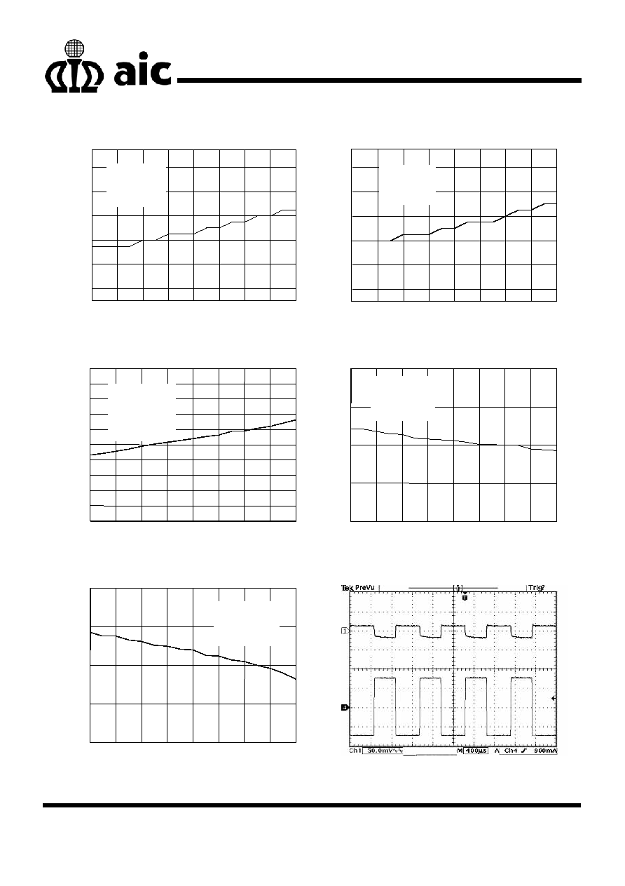
TYPICAL PERFORMANCE CHARACTERISTICS
Threshold Voltage
(V)
Temperature
(
�C)
Fig. 1 Turn-On Threshold vs. Temp.
-20
0
20
40
60
80
100
120
0.32
0.36
0.40
0.44
0.48
0.52
V
CNTL
=3.3V
V
IN
=2.5V
40
20
0
20
40
60
80
100
120
0.32
0.36
0.40
0.44
0.48
0.52
V
CNTL
=5V
V
IN
=2.5V
Thresho
l
d Voltage (V)
Temperature (
�C)
Fig. 2 Turn On Threshold vs. Temp.
O
u
tput Volt
age O
ffset (mV)
Temperature (
�C)
Fig. 3 Output Voltage Offset vs. Temp.
-40
-20
0
20
40
60
80
100
120
0.0
0.5
1.0
1.5
2.0
2.5
3.0
3.5
4.0
4.5
V
CNTL
=3.3V
V
IN
=2.5V
V
REF
=1.25V
No Load
Sourcin
g
C
u
rrent (A)
Temperature (
�C)
Fig. 4 Current-Limit (Sourcing) vs. Temp.
-40
-20
0
20
40
60
80
100
120
2
3
4
5
6
V
CNTL
=3.3V
V
IN
=2.5V
V
REF
=1.25V
Sinking C
u
rrent (A)
Temperature (
�C)
Fig. 5 Current-Limit (Sinking) vs. Temp.
-40
-20
0
20
40
60
80
100
120
2
3
4
5
6
V
CNTL
=3.3V
V
IN
=2.5V
V
REF
=1.25V
Fig. 6 Transient Response at 1.25V
TT
/3A
V
CNTL
=3.3V
V
IN
=2.5V, V
REF
=1.25V
V
OUT
, 50mV/div
I
OUT
,
2A/div
4

AIC1383B
TYPICAL PERFORMANCE CHARACTERISTICS
(Continued)
Fig. 7 Output Short-Circuit Protection (Sinking)
V
CNTL
=3.3V
V
IN
=2.5V
V
REF
=1.25V
Iout, 2A/div
Fig. 8 Output Short-Circuit Protection
(Sourcing)
V
CNTL
=3.3V
V
IN
=2.5V
V
REF
=1.25V
Iout, 2A/div
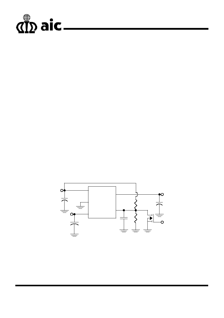
BLOCK DIAGRAM
VOUT
-
+
VOUT
GND
VIN
Control
VCNTL
Shutdown
Shutdown
Thermal
VREF
Current
Limit
5