AIC1520
Single High-Side Power Switch
Analog Integrations Corporation
4F, 9, Industry E. 9th Rd, Science Based Industrial Park, Hsinchu Taiwan, ROC
www.analog.com.tw
DS-1520-00 July 7, 00
TEL: 886-3-5772500
FAX: 886-3-5772510
1
n
FEATURES
∑ 120mW (5V Input) High-Side MOSFET Switch.
l
500mA Continuous Load Current.
l
80
mA Typical On-State Supply Current.
l
Current-Limit / Short Circuit Protection.
l
Thermal Limiting Protection under Overcurrent
Condition.
l
Undervoltage Lockout Ensures that Switch is off at
Start Up.
l
Output can be Forced Higher than Input (Off-State).
l
Slow Turn ON and Fast Turn OFF.
n
APPLICATIONS
l
Motherboard USB Management.
l
USB Power Management.
l
Hot Plug-In Power Supplies.
l
Battery-Charger Circuit.
l
Power Distribution Switch.
n
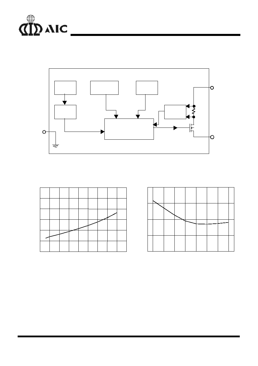
DESCRIPTION
The AIC1520 is an integrated high-side power
switch for self-powered and bus-powered
Universal Serial Bus (USB) applications. The
high-side switch is a MOSFET with 120m
W R
DS(ON)
,
which meets USB voltage drop requirements for
maximum transmission wire length.
Output current is typically limited to 1.0A, well
below the 5A safety requirement, and thermal
shutdown function shuts the switch off to prevent
damage under overcurrent conditions.
Guaranteed minimum output rise time limits
inrush current during hot plug-in, minimizing EMI
and preventing the voltage at upstream port from
dropping excessively.
n
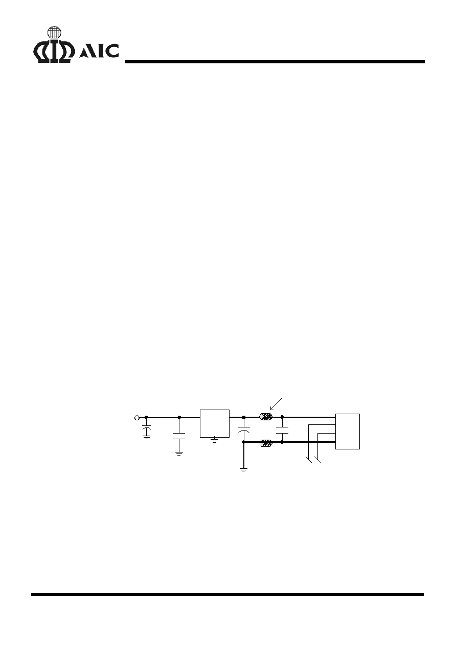
TYPICAL APPLICATION CIRCUIT
33
mF
5.0V
VCC
OUT
IN
GND
*
33
mF
D+
D-
GND
VBUS
0
.
01
mF
*
33
mF, 16V Tantalum, or
100
mF, 10V Electrolytic
Bold line indicate high-current traces
0.1
mF
Ferrite Bead
+
DATA
A
A
I
I
C
C
1
1
5
5
2
2
0
0
+
USB High-Side Power Switch
AIC1520
2
n
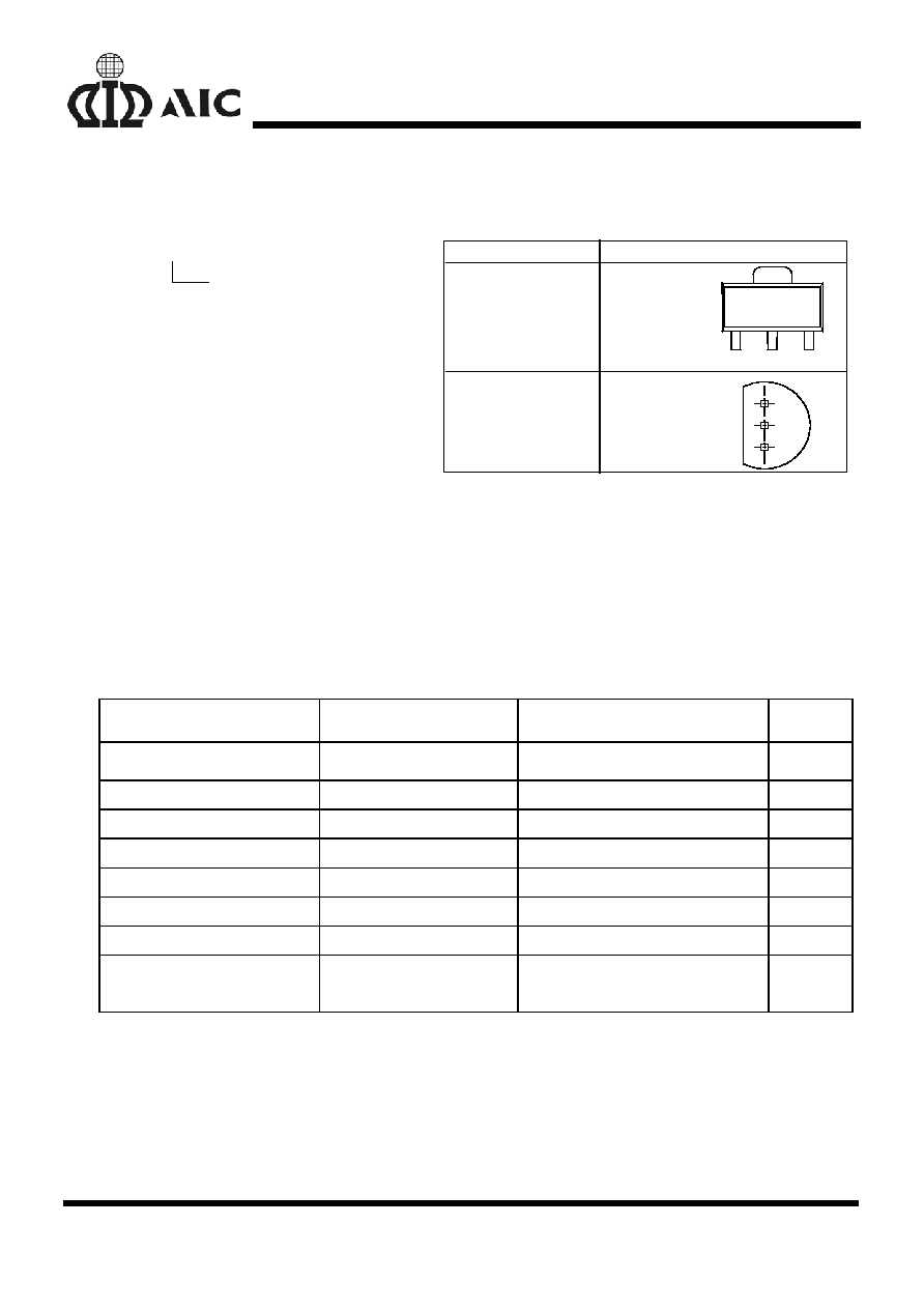
ORDERING INFORMATION
ORDER NUMBER
AIC1520CX
(SOT-89)
PIN CONFIGURATION
FRONT VIEW
1: IN
2: GND
3: OUT
AIC1520CX
1
2
3
1
2
3
PACKAGING TYPE
X: SOT-89
Z: TO-92
AIC1520CZ
(TO-92)
TOP VIEW
1: IN
2: GND
3: OUT
n
ABSOLUTE MAXIMUM RATINGS
Supply Voltage (V
IN
)
........................................................................................... 7.0V
Operating Temperature Range ............................................................... -40
∞C ~ 85∞C
Storage Temperature Range
............................................................... -65
∞C ~ 150∞C
n
ELECTRICAL CHARACTERISTICS
(V
IN
= 5V, Ta=25
∞C, unless otherwise
specified.)
PARAMETERS
CONDITIONS
MIN.
TYP.
MAX.
UNIT
Supply Current
Switch On, OUT=Open
80
100
mA
Output MOSFET Resistance
I
OUT
= 500mA
120
180
m
W
Output Turn-On Rise Time
R
L
= 10
W
500
mS
Output Turn-Off Fall Time
R
L
= 10
W
0.2
10
mS
Output Leakage Current
2
mA
Current Limit Threshold
0.6
1.0
1.25
A
Thermal Limit
110
∞C
UVLO Threshold
V
IN
Increasing
V
IN
Decreasing
2.8
2.6
V
AIC1520
4
n
TYPICAL PERFORMANCE CHARACTERISTICS
(Continued)
3.0
3.5
4.0
4.5
5.0
5.5
6.0
6.5
7.0
7.5
100
105
110
115
120
125
130
Output On Resistance vs. Supply Voltage
Switc
h
O
n
R
i
st
a
n
ce
(
m
W
)
Supply Voltage (V)
Sw
i
t
ch
O
n
R
e
si
st
a
n
ce
(
m
W
)
Temperature (
∞C)
-40
-20
0
20
40
60
80
100
80
90
100
110
120
130
140
150
Output On Resistance vs. Temperature
UV
LO Thre
s
hol
d V
o
l
t
age
(V
)
Temperature (
∞C)
-40
-20
0
20
40
60
80
100
2.4
2.5
2.6
2.7
2.8
2.9
3.0
Falling
Rising
UVLO Threshold Voltage vs. Temperature
Temperature (
∞C)
-40
-20
0
20
40
60
80
100
0.80
0.85
0.90
0.95
1.00
1.05
1.10
1.15
1.20
Current Limit Threshold vs. Temperature
Current
Li
m
i
t
(A
)
O
u
tput R
i
se
T
i
m
e
(m
S)
Temperature (
∞C)
Output Rise Time vs. temperature
-40
-20
0
20
40
60
80
100
350
400
450
500
550
V
IN
I
OUT
V
OUT
200mA/DIV
Turn On Rising Time (10
W loading)
AIC1520
5
n
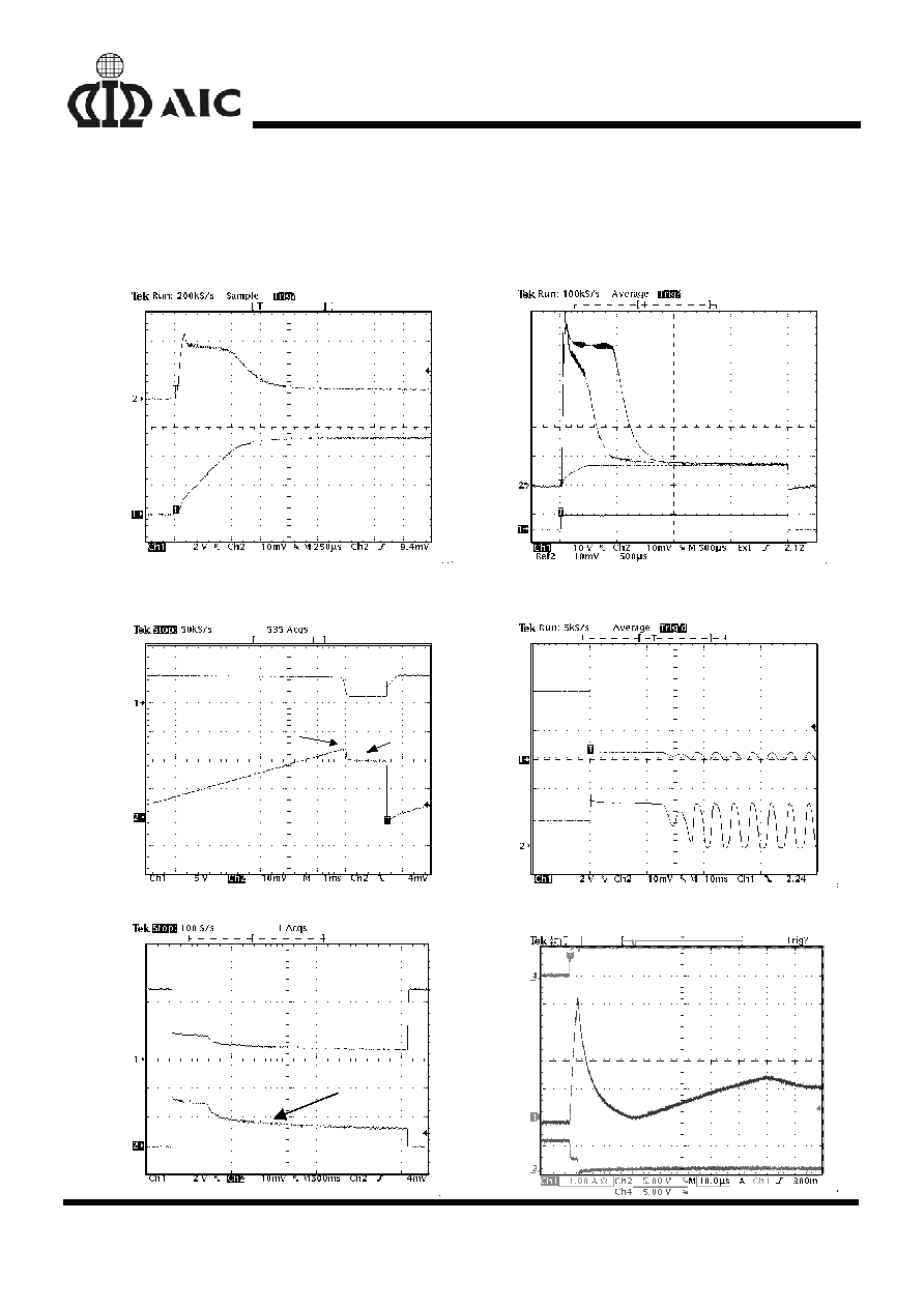
TYPICAL PERFORMANCE CHARACTERISTICS
(Continued)
500mA/div
V
OUT
I
OUT
Turn On Characteristic (35
W, 100mF Loading)
Turn On Characteristic (35
W Loading)
VIN
100
mF
no cap
I
OUT
, 200mA/div
220
mF
I
OUT
500mA/DIV
V
OUT
1A
1.2A
Current Limit Threshold
Short Circuit Testing
V
OUT
500mA/DIV
Thermal Oscillation
I
OUT
I
OUT
500mA/DIV
V
OUT
Thermal Limiting Transient Response
Thermal limit (2
W Loading)
Short Circuit Response Time
I
OUT
1A/DIV
Short
V
OUT