þÿ
AIC1520
USB High-Side Power Switch
Analog Integrations Corporation 4F, 9 Industry E. 9th Rd, Science-Based Industrial Park, Hsinchu, Taiwan
DS-1520-01 032502
TEL: 886-3-5772500
FAX: 886-3-5772510
www.analog.com.tw
1
n
FEATURES
·
120m
(5V Input) High-Side MOSFET Switch.
l
500mA Continuous Load Current.
l
80
µ
A Typical On-State Supply Current.
l
Current-Limit / Short Circuit Protection.
l
Thermal Limiting Protection under Overcurrent
Condition.
l
Undervoltage Lockout Ensures that Switch is off at
Start Up.
l
Output can be Forced Higher than Input (Off-State).
l
Slow Turn ON and Fast Turn OFF.
n
APPLICATIONS
l
Motherboard USB Management.
l
USB Power Management.
l
Hot Plug-In Power Supplies.
l
Battery-Charger Circuit.
l
Power Distribution Switch.
n
DESCRIPTION
The AIC1520 is an integrated high-side power
switch for self-powered and bus-powered Universal
Serial Bus (USB) applications. The high-side switch
is a MOSFET with 120m
R
DS(ON)
, which meets
USB voltage drop requirements for maximum
transmission wire length.
Output current is typically limited to 1.0A, well
below the 5A safety requirement, and thermal
shutdown function shuts the switch off to prevent
damage under overcurrent conditions.
Guaranteed minimum output rise time limits inrush
current during hot plug-in, minimizing EMI and
preventing the voltage at upstream port from
dropping excessively.
n
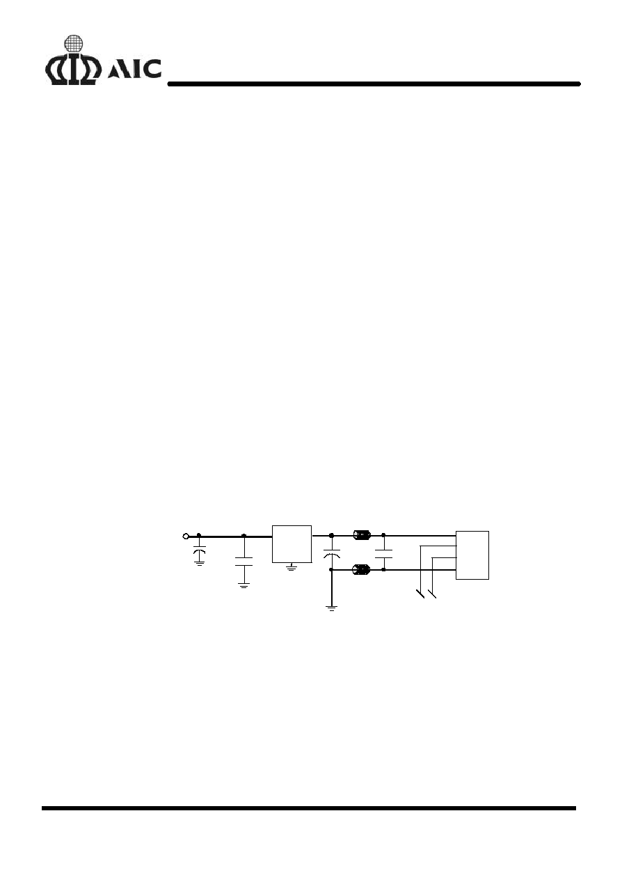
TYPICAL APPLICATION CIRCUIT
33
µ
F
5.0V
VCC
OUT
IN
GND
*
33
µ
F
D+
D-
GND
VBUS
0
.
01
µ
F
*
33
µ
F, 16V Tantalum, or
100
µ
F, 10V Electrolytic
Bold line indicate high-current traces
0.1
µ
F
Ferrite Bead
+
DATA
AIC1520
+
USB High-Side Power Switch
AIC1520
2
n
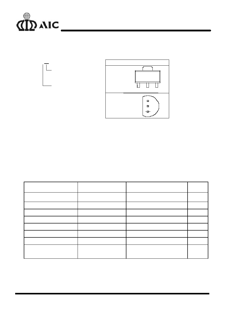
ORDERING INFORMATION
SOT-89
TOP VIEW
1: IN
2: GND
3: OUT
PIN CONFIGURATION
AIC1520CXXX
1
2
3
1
2
3
TO-92
TOP VIEW
1: I N
2: GND
3: OUT
Example: AIC1520CXTR
à
in SOT-89 Package & Taping &
Reel Packing Type
PACKING TYPE
TR: TAPE & REEL
BG: BAG
PACKAGING TYPE
X: SOT-89
Z: TO-92
n
ABSOLUTE MAXIMUM RATINGS
Supply Voltage (V
IN
) .......................................................... ... ... ... .......... ... ........... 7.0V
Operating Temperature Range
......... ... ... ................. ... ... ... ... .... ............... -40
°
C ~ 85
°
C
Storage Temperature Range
....................................... ... ... .................. -65
°
C ~ 150
°
C
n
ELECTRICAL CHARACTERISTICS
(V
IN
= 5V, T
A
=25
°
C, unless otherwise
specified.)
PARAMETERS
CONDITIONS
MIN.
TYP.
MAX.
UNIT
Supply Current
Switch On, OUT=Open
80
100
µ
A
Output MOSFET Resistance
I
OUT
= 500mA
120
180
m
Output Turn-On Rise Time
R
L
= 10
500
µ
S
Output Turn-Off Fall Time
R
L
= 10
0.2
10
µ
S
Output Leakage Current
2
µ
A
Current Limit Threshold
0.6
1.0
1.25
A
Thermal Limit
110
°
C
UVLO Threshold
V
IN
Increasing
V
IN
Decreasing
2.8
2.6
V
AIC1520
3
n
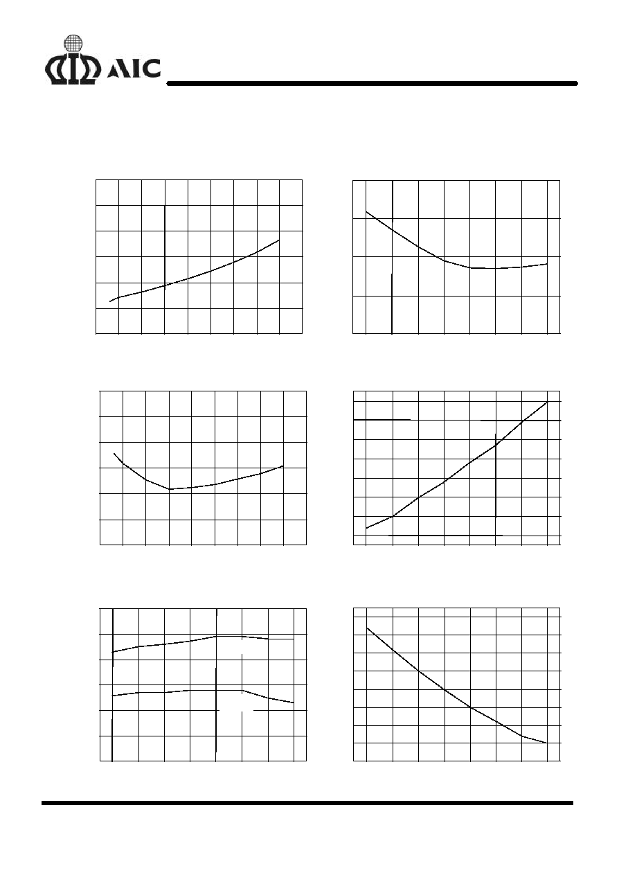
TYPICAL PERFORMANCE CHARACTERISTICS
3.0
3.5
4.0
4.5
5.0
5.5
6.0
6.5
7.0
7.5
60
65
70
75
80
85
90
Fig. 1 On-State Supply Current vs. Supply
Supply Current (
µ
A)
Supply Voltage (V)
-
40
-20
0
20
40
60
80
100
65
70
75
80
85
Fig. 2 On-State Supply Current vs. Temperature
Supply Current (
µ
A)
Temperature (
°
C)
3.0
3.5
4.0
4.5
5.0
5.5
6.0
6.5
7.0
7.5
100
105
110
115
120
125
130
Fig. 3 Output On Resistance vs. Supply Voltage
Switch
On
Ristance (m
)
Supply Voltage (V)
Switch On Resistance (m
)
Temperature (
°
C)
-40
-20
0
20
40
60
80
100
80
90
100
110
120
130
140
150
Fig. 4 Output On Resistance vs. Temperature
UVLO Threshold Voltage (V)
Temperature (
°
C)
-40
-20
0
20
40
60
80
100
2.4
2.5
2.6
2.7
2.8
2.9
3.0
Falling
Rising
Fig. 5 UVLO Threshold Voltage vs. Temperature
Temperature (
°
C)
-40
-20
0
20
40
60
80
100
0.80
0.85
0.90
0.95
1.00
1.05
1.10
1.15
1.20
Fig. 6 Current Limit Threshold vs. Temperature
Current Limit (A)
AIC1520
4
n
TYPICAL PERFORMANCE CHARACTERISTICS
(Continued)
Output Rise Time (
µ
S)
Temperature (
°
C)
Fig. 7 Output Rise Time vs. temperature
-40
-20
0
20
40
60
80
100
350
400
450
500
550
V
IN
I
OUT
V
OUT
200mA/DIV
Fig. 8 Turn On Rising Time (10
loading)
500mA/di
v
V
OUT
I
OUT
Fig. 9 Turn On Characteristic (35
, 100
µ
F Loading)
VIN
100
µ
F
no cap
I
OUT
, 200mA/div
220
µ
F
Fig. 10 Turn On Characteristic (35
Loading)
I
OUT
500mA/DIV
V
OUT
1A
1.2A
Fig. 11 Current Limit Threshold
Fig. 12 Short Circuit Testing
V
OUT
500mA/DIV
Thermal Oscillation
I
OUT
AIC1520
5
n
TYPICAL PERFORMANCE CHARACTERISTICS
(Continued)
I
OUT
500mA/DIV
V
OUT
Fig. 13 Thermal Limiting Transient Response
Thermal limit (2
Loading)
Fig. 14 Short Circuit Response Time
I
OUT
1A/DIV
Short
V
OUT
n
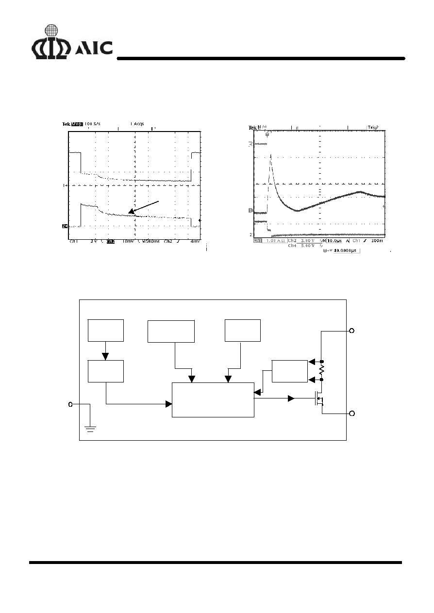
BLOCK DIAGRAM
GATE
NMOS
RS
Limit
Current
UVLO
Gate Control
Charge
Pump
Thermal
Protection
OSC.
GND
OUT
IN
n
PIN DESCRIPTIONS
PIN 1: IN
- Power supply input.
PIN 2: GND
- Chip power ground.
PIN 3: OUT
- MOSFET switch output.

AIC1520
6
n
APPLICATION INFORMATIONS
Current Limit
The current limit threshold is preset internally. It
protects the output MOSFET switches from
damage due to undesirable short circuit conditions
or excess inrush current often encountered during
hot plug-in. AIC1520 allows a minimum current of
0.5A through the MOSFET switches.
Thermal Protection
When the chip temperature exceeds 110
°
C, the
thermal protection function works.
Supply Filtering
A 0.1
µ
F to 1
µ
F bypass capacitor from IN to GND,
located near the device, is strongly recommended
to control supply transients. Without a bypass
capacitor, an output short may cause sufficient
ringing on the input (from supply lead inductance)
to damage internal control circuitry.
Transient Drop Requirements
The USB supports dynamic attachment (hot plug-
in) of peripherals. A current surge is caused by the
input capacitance of downstream device. Ferrite
beads are recommended in series with all power
and ground connector pins. Ferrite beads reduce
EMI and limit the inrush current during hot-
attachment by filtering high-frequency signals.
Short Circuit Transient
Bulk capacitance provides the short-term transient
current needed during a hot-attachment event.
With a 33uF, 16V tantalum or 100uF, 10V
electrolytic capacitor mounted close to
downstream connector should provide transient
drop protection.
Printed Circuit Layout
The power circuitry of USB printed circuit boards
requires a customized layout to maximize thermal
dissipation and to minimize voltage drop and EMI.
AIC1520
7
n
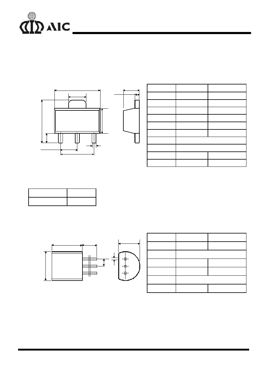
PHYSICAL DIMENSIONS
l
SOT-89 (unit: mm)
SYMBOL
MIN
MAX
A
1.40
1.60
B
0.36
0.48
C
0.35
0.44
D
4.40
4.60
D1
1.62
1.83
E
2.29
2.60
e
1.50 (TYP.)
e1
3.00 (TYP.)
H
3.94
4.25
B
e
H
e1
D
D1
A
C
L
E
L
0.89
1.20
l
SOT-89 MARKING
Part No.
Marking
AIC1520-CX
BG01
l
TO-92 (unit: mm)
SYMBOL
MIN
MAX
A
4.32
5.33
C
0.38 (TYP.)
D
4.40
5.20
E
3.17
4.20
e1
1.27 (TYP.)
A
L
e1
D
C
E
L
12.7
-