AIC1526
Dual USB High-Side Power Switch
Analog Integrations Corporation
4F, 9, Industry E. 9th Rd, Science Based Industrial Park, Hsinchu Taiwan, ROC
www.analog.com.tw
DS-1526-00
TEL: 886-3-5772500
FAX: 886-3-5772510
1
FEATURES
∑ 110m (5V Input) High-Side MOSFET Switch.
500mA Continuous Load Current per Channel.
110
µA Typical On-State Supply Current.
1
µA Typical Off-State Supply Current.
Current-Limit / Short Circuit Protection.
Thermal Shutdown Protection under Overcurrent
Condition.
Undervoltage Lockout Ensures that Switch is off at
Start Up.
Output can be Forced Higher than Input (Off-
State).
Open-Drain Fault Flag.
Slow Turn ON and Fast Turn OFF.
Enable Active-High or Active-Low.
APPLICATIONS
USB Power Management.
Hot Plug-In Power Supplies.
Battery-Charger Circuit.
DESCRIPTION
The AIC1526 is a dual high-side power switch
for self-powered and bus-powered Universal
Serial Bus (USB) applications. One high-side
switch is a MOSFET with 110m
R
DS(ON)
, which
meets USB voltage drop requirements for
maximum transmission wire length.
Multi-purpose open-drain fault flag output
indicates over-current limiting, thermal
shutdown, or undervoltage lockout for each
channel. Output current is typically limited to 1A,
well below the 5A safety requirement, and the
thermal shutdown function independently
controls each channel under overcurrent
condition.
Guaranteed minimum output rise time limits
inrush current during hot plug-in, minimizing
EMI and preventing the voltage at upstream port
from dropping excessively.

AIC1526
2
TYPICAL APPLICATION CIRCUIT
D+
D-
GND
VBUS
OVERCURRENT
IN
OUTA
GND
CTLA
FLGA
FLGB
CTLB OUTB
AIC1526
USB Controller
GND
ON/OFF
4.50V to 5.25V
Upstream VBUS
100mA max
DATA
D+
D-
GND
VBUS
0.01
µF
33
µF
*
+
DATA
0.01
µF
33
µF
*
+
DATA
0.1
µF
10K
10K
33
µF
5.0V
VCC
Ferrite
Bead
OVERCURRENT
VIN
ON
/
D+
D-
GND
VBUS
AIC1722
OUT
IN
GND
+
1
µF
C
IN
10
µF
C
OUT
+
+
*
33
µF, 16V Tantalum, or
100
µF, 10V Electrolytic
Bold line indicate high- current traces
Two-Port Self-Powered Hub
ORDERING INFORMATION
ORDER NUMBER
AIC1526-0CN
AIC1526-1CN
(PLASTIC DIP)
PIN CONFIGURATION
TOP VIEW
PACKAGE TYPE
N: PLASTIC DIP
S: SMALL OUTLINE
TEMPERATURE RANGE
C: 0
∞C~+70∞C
CONTROL POLARITY
0: ACTIVE LOW
1: ACTIVE HIGH
AIC1526-XXX
AIC1526-0CS
AIC1526-1CS
(PLASTIC SO)
GND
OUTA
IN
OUTB
FLGB
FLGA
CTLB
CTLA 1
3
4
2
8
6
5
7
ABSOLUTE MAXIMUM RATINGS
Supply Voltage (V
IN
)
........................................................................................... 7.0V
Fault Flag Voltage (V
FLG
) ....................................................................................... 7.0V
Fault Flag Current (I
FLG
)
................................................................................. 50mA
Control Input (V
CTL
)
................................................................................. -0.3V ~15V
Operating Temperature Range .................................................................-20
∞C~80∞C
Storage Temperature Range
............................................................... -65
∞C ~ 150∞C

AIC1526
3
TEST CIRCUIT
10
AIC1526
0.1
µF
C1
OFF
ON
V
CC
+5V
10K R1
R4
R4
CTLA
OUTA
FLGA
IN
FLGB
GND
CTLB
OUTB
OFF
ON
10
10K R2
ELECTRICAL CHARACTERISTICS
(V
IN
= 5V, Ta=25
∞
∞
∞
∞C, unless otherwise specified.)
PARAMETERS
CONDITIONS
MIN.
TYP.
MAX.
UNIT
Supply Current
V
CTL
=Logic "0" , OUT=Open
V
CTL
=Logic "1" , OUT=Open
0.75
110
5
160
µA
Control Input Voltage
V
CTL
=Logic "0"
V
CTL
=Logic "1"
2.4
0.8
V
Control Input Current
V
CTL
=Logic "0"
V
CTL
=Logic "1"
0.01
0.01
1
1
µA
Control Input Capacitance
1
pF
Output MOSFET Resistance
110
150
m
Output Turn-On Rise Delay
R
L
= 10
each Output
100
µS
Output Turn-On Rise Time
R
L
= 10
each Output
1000
2500
µS
Output Turn-Off Delay
R
L
= 10
each Output
0.8
20
µS
Output Turn-Off Fall Time
R
L
= 10
each Output
0.7
20
µS
Output Leakage Current
10
µA
Current Limit Threshold
0.6
1.0
1.25
A
Overtemperature Shutdown
Threshold
T
J
Increasing
T
J
Decreasing
135
125
∞C
Error Flag Output Resistance
V
IN
= 5V , I
L
=10 mA
V
IN
= 3.3V , I
L
=10mA
10
15
25
40
Error Flag Off Current
V
FLG
= 5V
0.01
1
µA
UVLO Threshold
V
IN
Increasing
V
IN
Decreasing
2.6
2.4
V
AIC1526
4
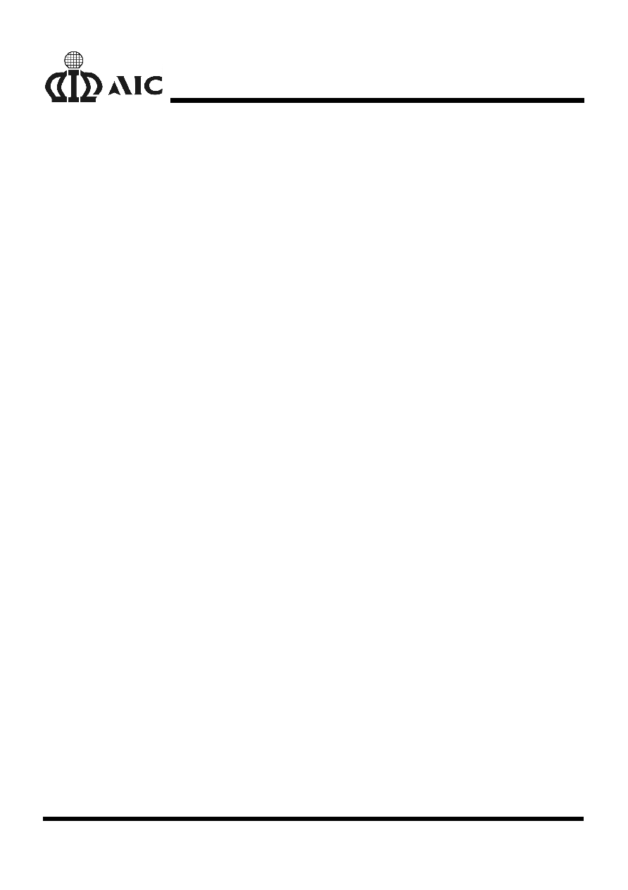
BLOCK DIAGRAM
CTLB
FLGB
FLGA
CTLA
OUTA
CHARGE PUMP
THERMAL
SHUTDOWN
CHARGE PUMP
DRIVER
UVLO
CURRENT
LIMIT
DRIVER
IN
P
O
W
E
R N-
M
O
S
F
E
T
CURRENT
LIMIT
OUTB
P
O
W
E
R N-
M
O
S
F
E
T
CS
CS
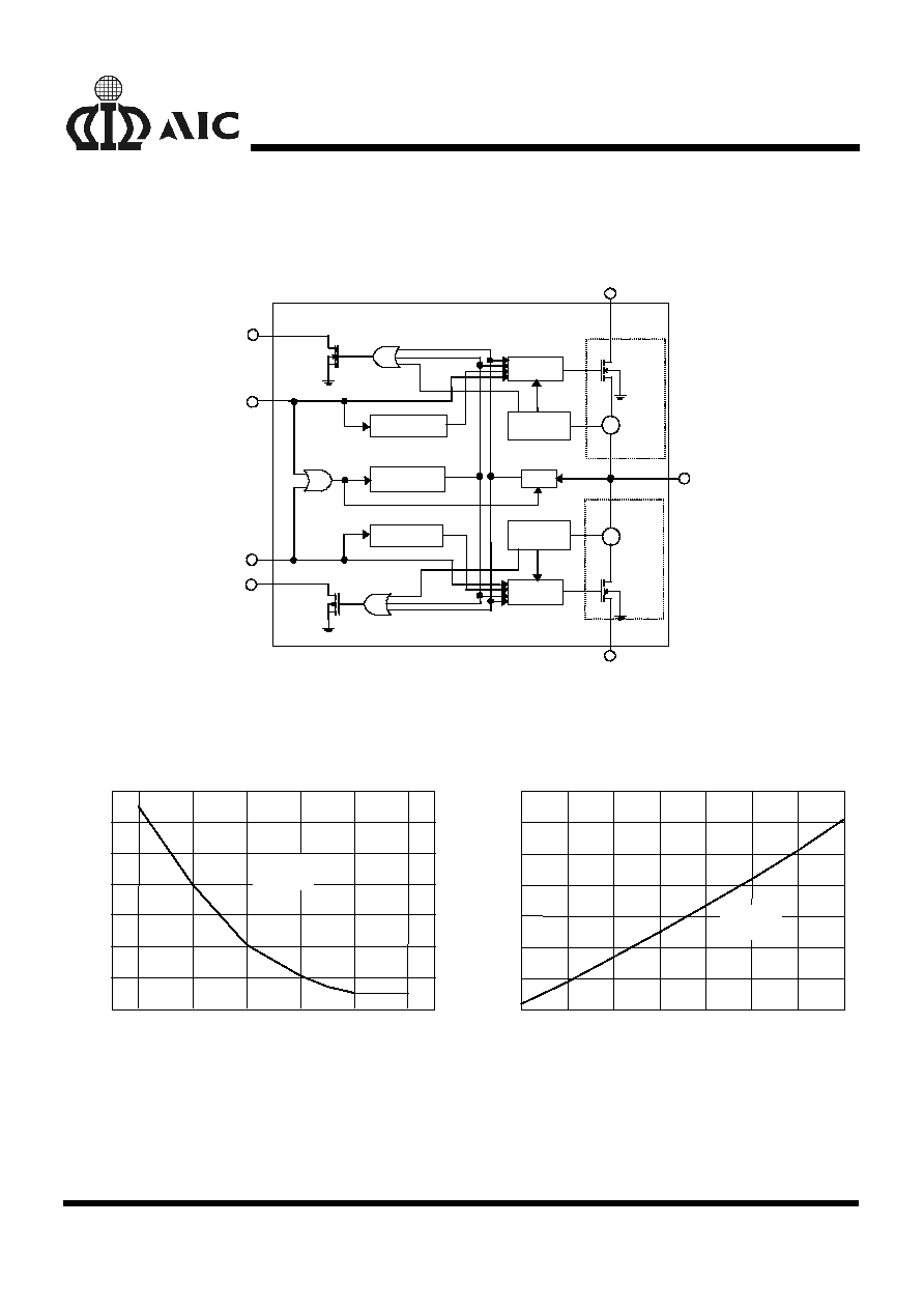
TYPICAL PERFORMANCE CHARACTERISTICS
ON Resistance vs. Supply Voltage
O
N
R
e
si
stan
ce
(
m
)
Supply Voltage (V)
3.0
3.5
4.0
4.5
5.0
5.5
104
106
108
110
112
114
116
118
RL=47
T=25
∞C
Temperature (
∞C)
Output On Resistance vs. Temperature
-40
-20
0
20
40
60
80
100
80
90
100
110
120
130
140
150
O
N
R
e
si
stan
ce
(
m
)
RL=47
T=25
∞C
AIC1526
5
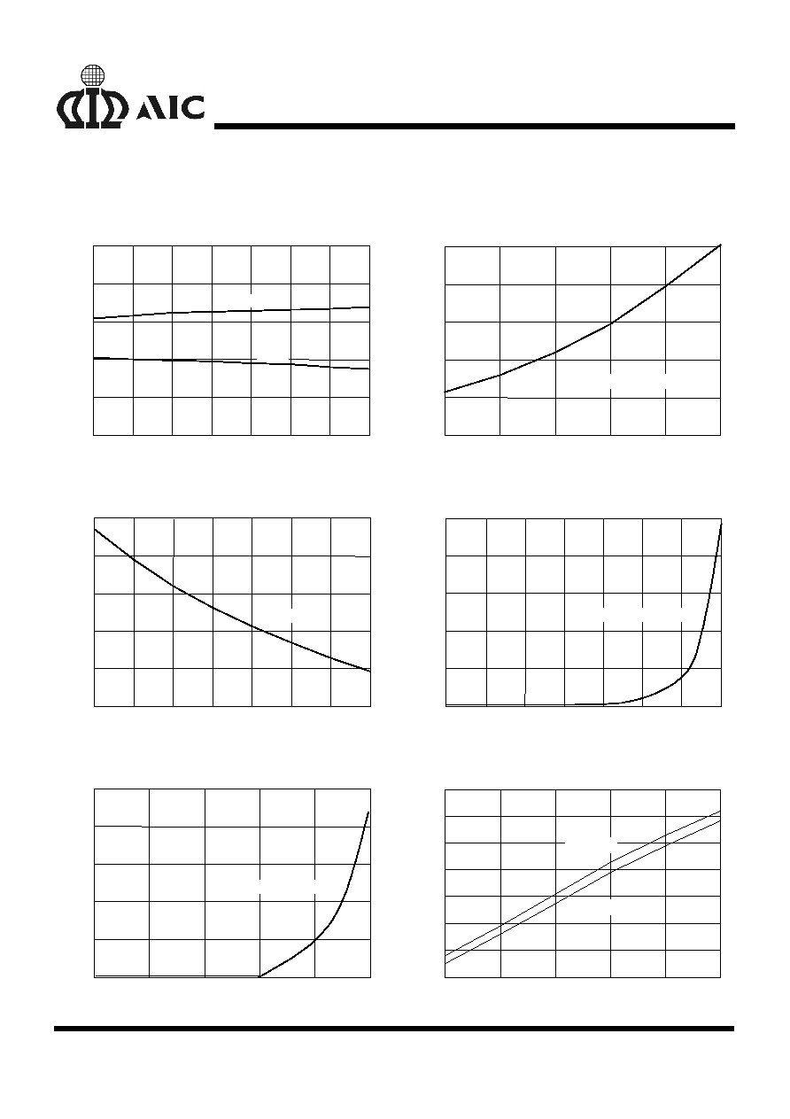
TYPICAL PERFORMANCE CHARACTERISTICS
(Continued)
UVLO Threshold Voltage vs. Temperature
Temperature (
∞C)
T
h
r
e
s
h
o
l
d
V
o
l
t
ag
e (
V
)
-40
-20
0
20
40
60
80
100
2.0
2.2
2.4
2.6
2.8
3.0
Rising
Falling
ON State Supply Current vs. Supply Voltage
Supply Voltage (V)
3
4
5
6
7
8
60
80
100
120
140
160
Both Switches ON
S
u
p
p
l
y
C
u
rre
n
t
(
µ
A)
-40
-20
0
20
40
60
80
100
80
90
100
110
120
130
Both Switches ON
OFF State Current vs. Temperature
Temperature (
∞C)
S
u
ppl
y
C
u
r
r
e
nt
(
µ
A)
OFF State Current vs. Temperature
Temperature (
∞C)
Suppl
y C
u
rre
nt (
µ
A)
-40
-20
0
20
40
60
80
100
0
0.02
0.04
0.06
0.08
0.10
Both Switches OFF
OFF State Current vs. Supply Voltage
Supply Voltage (V)
3
4
5
6
7
8
0
0.02
0.04
0.06
0.08
0.10
Both Switches
S
uppl
y
C
u
r
r
e
nt
(
µ
A)
Control Threshold vs. Supply Voltage
Supply Voltage (V)
E
n
a
b
le
v
o
lt
a
g
e
3.0
3.5
4.0
4.5
5.0
5.5
1.0
1.1
1.2
1.3
1.4
1.5
1.6
1.7
V
EN
Rising
V
EN
Falling