AIC1567
5-bit DAC, Synchronous PWM Power Regulator
with Linear Controller
Analog Integrations Corporation
4F, 9, Industry E. 9th Rd, Science Based Industrial Park, Hsinchu Taiwan, ROC
www.analog.com.tw
DS-1567-00
TEL: 886-3-5772500
FAX: 886-3-5772510
1
FEATURES
Switching Regulator and Low Dropout Linear
Regulator on single chip.
Simple Voltage-Mode PWM Control.
Dual N-Channel MOSFET Synchronous Drive.
Fast Transient Response.
±1.0% 5-Bit Digital-to-Analog Output Voltage.
Adjustable Current Limit Without External Sense
Resistor.
Full 0% to 100% Duty Ratio.
200KHz Free-Running Oscillator Programmable
up to 350KHz.
Power-Good Output Voltage Monitor.
Short Circuit Protection with Low Short Circuit
Output Current.
APPLICATIONS
Power Supply for Pentium II, Power PC and
Alpha Microprocessors.
High-Power 5V to 3.xV DC/DC Regulators.
Low-Voltage Distributed Power Supplies.
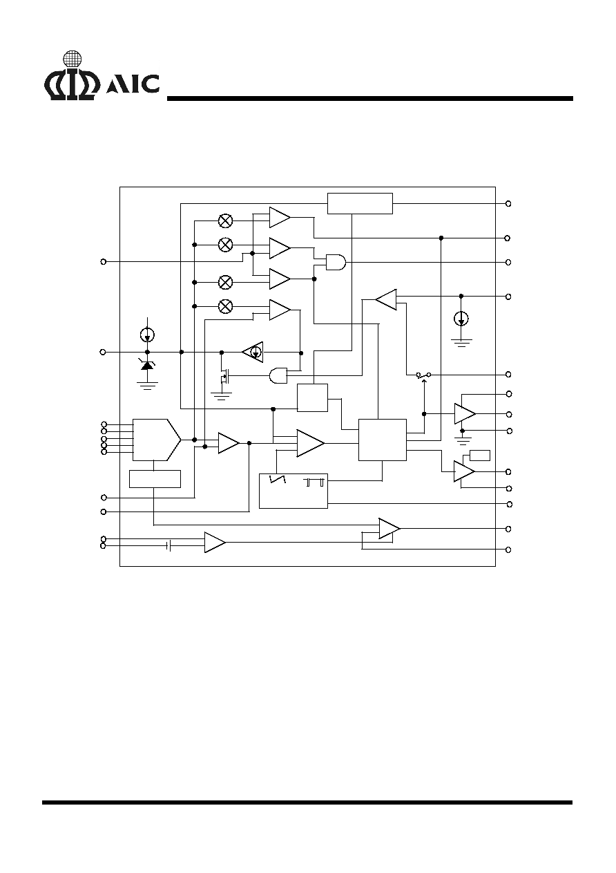
DESCRIPTION
The AIC1567 is a high power, high efficiency
switching regulator controller optimized for high
performance microprocessor applications. It is
designed to drive dual N-channel MOSFET in a
standard synchronous buck topology.
Featuring a low dropout linear regulator and a
digitally programmable switching regulator, the
AIC1567 includes monitoring and protection
capabilities in addition to all the essential
synchronous PWM control functions.
The internal 5-bit Digital-to-Analog Converter
(DAC) adjusts the output voltage from 2.0V to
3.5V in 0.1V increments and 1.3V to 2.0V in
0.05V increments. The precision reference and
voltage-mode control can provide output
regulation within
±1.0% over temperature and
line voltage shifts.
The internal oscillator of the AIC1567 free-runs
at 200KHz and can be adjusted up to 350KHz.
The resulting PWM duty ratio ranges from 0% to
100%. The error amplifier features a 11MHz
bandwidth and 6V/
µS slew rate, which enables
high converter bandwidth for fast transient
response.
AIC1567
3
ABSOLUTE MAXIMUM RATINGS
Supply Voltage, V
CC
................................................................................................... 15V
Boot Voltage, V
BOOT
................................................................................................. 15V
Input, Output, or I/O Voltage ................................................... GND - 0.3V to VCC+0.3V
ESD Classification
............................................................................................ Class 2
Recommended Operating Conditions
Supply Voltage, V
CC
......................................................................................... 12V
±10%
Ambient Temperature Range ........................................................................ 0
∞C ~ 70∞C
Junction Temperature Range ...................................................................... 0
∞C ~100∞C
Thermal Information
Thermal Resistance,
JA
(Typical, Note 1)
SOIC Package ..................................................................................... 100
∞C/W
SOIC Package (with 3 in
2
of Copper) .................................................. 90
∞C/W
Maximum Junction Temperature (Plastic Package) ............................................. 150
∞C
Maximum Storage Temperature Range .................................................. -65
∞C~150∞C
Maximum Lead Temperature (Soldering 10 sec) ................................................ 300
∞C
Note 1: symbol
JA
is measured with the component mounted on an evaluation PC board in free air.
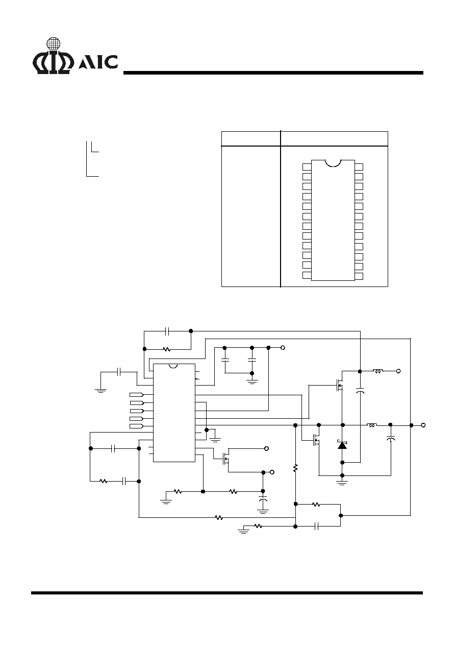
TEST CIRCUIT
Refer to TYPICAL APPLICATION CIRCUIT.
ELECTRICAL CHARACTERISTICS
(VCC= 12V, Ta=25
∞
∞
∞
∞C, unless otherwise
specified.)
PARAMETER
TEST CONDITIONS
SYMBOL MIN.
TYP.
MAX.
UNIT
VCC Supply Current
Nominal Supply
UGATE Open
I
VCC
2
mA
Power-On Reset
V
CC
Threshold
V
OCSET
=4.5V
7
8.5
V
Rising V
OCSET
Threshold
1.26
V
Oscillator
Free Running Frequency
R
T
Open
170
200
230
KHz
Total Variation
6K
< R
T
<200K
-20
+20
%
Ramp Amplitude
R
T
Open
V
OSC
1.5
V
P-P
AIC1567
4
ELECTRICAL CHARACTERISTICS
(Continued)
PARAMETER
TEST CONDITIONS
SYMBOL
MIN.
TYP.
MAX.
UNIT
Reference and DAC
DACOUT Voltage Accuracy
V
DAC
=1.8V ~3.5V
-1.0
+1.0
%
Error Amplifier
DC Gain
76
dB
Gain-Bandwidth Product
GBW
11
MHz
Slew Rate
SR
6
V/
µS
Gate Driver
Upper Gate Source
R
UGATE
8.0
12
Upper Gate Sink
R
UGATE
5.5
10
Lower Gate Source
R
LGATE
8.0
12
Lower Gate Sink
R
LGATE
5.5
10
Protection
Over-Voltage Trip (V
SEN/DACOUT
)
106
115
125
%
OCSET Current Source
V
OCSET
=4.5VDC
I
OCSET
170
200
230
µA
OVP Sourcing Current
V
VSEN
=5.5V, V
OVP
=0V
I
OVP
30
mA
Soft Start Current
I
SS
10
µA
Soft Start Sink Current under
Current Limit
V
VSEN
=V
DAC
, V
OCSET
=5.0V,
V
PHASE
=0V,
V
FB
=VDAC=50mV
130
µA
Soft Start Sink Current under
Hard Current Limit
V
VSEN
=0, V
OCSET
=5.0V,
V
PHASE
=0V, V
FB
=0V
65
mA
Power Good
Upper Threshold (V
VSEN
/V
DAC
) V
VSEN
Rising
106
114
%
Lower Threshold (V
VSEN
/ V
DAC
) V
VSEN
Falling
84
94
%
Hysteresis (V
VSEN
/ V
DAC
)
Upper and Lower Threshold
2
%
PGOOD Voltage Low
I
PGOOD
=5mA
V
PGOOD
0.5
V
Linear Regulator
VLFB Feedback Voltage
1.18
1.21
1.24
V
VLFB Bias Current
40
nA
LIDRI Sourcing Current
10
mA
Current Limiting Threshold
10
20
30
mV