
AIC1569A
5-bit DAC, Synchronous PWM Power Regulator
Analog Integrations Corporation
4F, 9, Industry E. 9th Rd, Science Based Industrial Park, Hsinchu Taiwan, ROC
www.analog.com.tw
DS-1569A-00
TEL: 886-3-5772500
FAX: 886-3-5772510
1
FEATURES
Compatible with HIP6004.
Simple Voltage-Mode PWM Control.
Dual N-Channel MOSFET Synchronous Drive.
Fast Transient Response.
±1% 5-Bit Digital-to-Analog Output Voltage.
Adjustable Current Limit Without External
Sense Resistor.
Full 0% to 100% Duty Ratio.
200KHz Free-Running Oscillator,
Programmable up to 350KHz.
Power-Good Output Voltage Monitor.
APPLICATIONS
Power Supply for PentiumÆ II, PowerÆ and
AlphaÆ Microprocessors.
High-Power 5V to 3.xV DC/DC Regulators.
Low-Voltage Distributed Power Supplies.
DESCRIPTION
The AIC1569A is a high power, high efficiency
switching regulator controller optimized for high
performance microprocessor applications. It is
designed to drive dual N-channel MOSFETs in a
standard synchronous buck topology. Featuring
a digitally programmable switching regulator, the
AIC1569A includes monitoring and protection
capabilities in addition to all the essential
synchronous PWM control functions.
The internal 5-bit Digital-to-Analog Converter
(DAC) adjusts the output voltage from 2.0V to
3.5V in 0.1V increments and 1.3V to 2.0V in
0.05V increments. The precision reference and
voltage-mode control can provide output
regulation within
±1% over temperature and line
voltage shifts.
The internal oscillator of the AIC1569A free-runs
at 200KHz and can be adjusted up to 350KHz.
The resulting PWM duty ratio ranges from 0% to
100%. The error amplifier features an 11MHz
bandwidth and 6V/
µS slew rate, which enables
high converter bandwidth for fast transient
response.
The AIC1569A provides adjustable over current
and short circuit protections. It senses the output
current across the on resistance of the upper N-
channel MOSFET without an external low value
sense resistor. It also monitors the output voltage
with a window comparator and issues a power
good signal when the output is within 10% of the
rated output voltage.

AIC1569A
2
ORDERING INFORMATION
AIC1569A XX
TOP VIEW
PIN CONFIGURATION
ORDER NUMBER
PACKAGE TYPE
S: SMALL OUTLINE
TEMPERATURE RANGE
C: 0
∞C~70∞C
AIC1569ACS
(PLASTIC SO)
RT
OVP
VCC
LGATE
PGND
BOOT
UGATE
PHASE
PGOOD
GND
20
19
18
17
16
15
14
13
12
11
1
2
3
4
5
6
7
8
9
10
VSEN
OCSET
SS
VID0
VID1
VID2
VID3
VID4
COMP
FB
TYPICAL APPLICATION CIRCUIT
AIC1569A
RT
OVP
VCC
LGATE
PGND
BOOT
UGATE
PHASE
PGOOD
GND
OCSET
COMP
FB
SS
VID0
VID1
VID2
VID3
VID4
VSEN
C8
0.1
µF
C6
1000pF
C7
33pF
C9
1000pF
+
C3
1000
µF x 3
R2
2.2K
R6
90.9K
L1
1
µH
M1
RF
P4
5
N
0
3
L
R5
3.01K
VID0
VID1
VID2
VID3
VID4
5V
R7
1.2M
C5
0.1
µF
+
C4
1000
µF x 8
R4
15K
R3
47K
1N
58
20
M2
NDP603AL
C1
1
µF
12V
C2
0.1
µF
R1
47
D1
L2
3
µH
V
OUT
DC/DC Converter for Pentium
II V
CORE
AIC1569A
3
ABSOLUTE MAXIMUM RATINGS
Supply Voltage, V
CC
...................................................................................................... 15V
Boot Voltage, V
BOOT
..................................................................................................... 15V
Input, Output, or I/O Voltage ....................................................... GND - 0.3V to VCC+0.3V
ESD Classification ................................................................................................... Class 2
Recommended Operating Conditions
Supply Voltage, V
CC
............................................................................................. 12V
±10%
Ambient Temperature Range ............................................................................ 0
∞C ~ 70∞C
Junction Temperature Range ........................................................................... 0
∞C ~100∞C
Thermal Information
Thermal Resistance,
JA
(Typical, Note 1)
SOIC Package......................................................................................... 100
∞C /W
SOIC Package (with 3 in
2
of Copper) ....................................................... 90
∞C /W
Maximum Junction Temperature (Plastic Package) ................................................ 150
∞C
Maximum Storage Temperature Range ..................................................... -65
∞C ~150∞C
Maximum Lead Temperature (Soldering 10 sec) ................................................. 300
∞C
Note 1:
JA
is measured with the component mounted on an evaluation PC board in free air.
TEST CIRCUIT
Refer to TYPICAL APPLICATION CIRCUIT.
ELECTRICAL CHARACTERISTICS
(VCC= 12V, Ta=25
∞
∞
∞
∞C, unless otherwise specified.)
PARAMETER
TEST CONDITIONS
SYMBOL
MIN.
TYP.
MAX.
UNIT
VCC Supply Current
Nominal Supply
UGATE Open
I
VCC
1
3
mA
Power-On Reset
V
CC
Threshold
V
OCSET
=4.5V
8.2
9.3
10.2
V
Rising V
OCSET
Threshold
1.26
V
Oscillator
Free Running Frequency
RT Open
170
200
230
KHz
Total Variation
6K
<R
T
<200K
-20
+20
%
Ramp Amplitude
RT Open
V
OSC
1.5
V
P-P
AIC1569A
4
ELECTRICAL CHARACTERISTICS
(Continued)
PARAMETER
TEST CONDITIONS
SYMBOL
MIN.
TYP.
MAX.
UNIT
DAC Output Voltage
DAC Output Voltage Accuracy
VDAC=1.3V~3.5V
-1.0
+1.0
%
Error Amplifier
DC Gain
76
dB
Gain-Bandwidth Product
GBW
11
MHz
Slew Rate
SR
6
V/
µS
Gate Driver
Upper Gate Source
R
UGATE
5.8
12
Upper Gate Sink
R
UGATE
4.4
10
Lower Gate Source
R
LGATE
4.7
12
Lower Gate Sink
R
LGATE
3.0
10
Protection
Over-Voltage Trip (V
VSEN
/VDAC)
106
115
125
%
OCSET Current Source
V
OCSET
=4.5VDC
I
OCSET
170
200
230
µA
OVP Sourcing Current
V
VSEN
=5.5V, V
OVP
=0V
I
OVP
30
mA
SS Current
I
SS
10
µA
SS Voltage under Current Limit
V
VSEN
=VDAC,
V
OCSET
=5.0V, V
PHASE
=0V,
V
FB
=VDAC
- 50mV
2.0
V
SS Voltage under Hard Current
Limit
V
VSEN
=0, V
OCSET
=5.0V,
V
PHASE
=0V, V
FB
=0V
0.7
V
Power Good
Upper Threshold (V
VSEN
/VDAC
)
V
VSEN
Rising
106
114
%
Lower Threshold (V
VSEN
/VDAC
)
V
VSEN
Falling
84
94
%
Hysteresis (V
VSEN
/VDAC
)
Upper and Lower
threshold
2
%
PGOOD Voltage Low
I
PGOOD
=5mA
V
PGOOD
0.5
V
AIC1569A
5
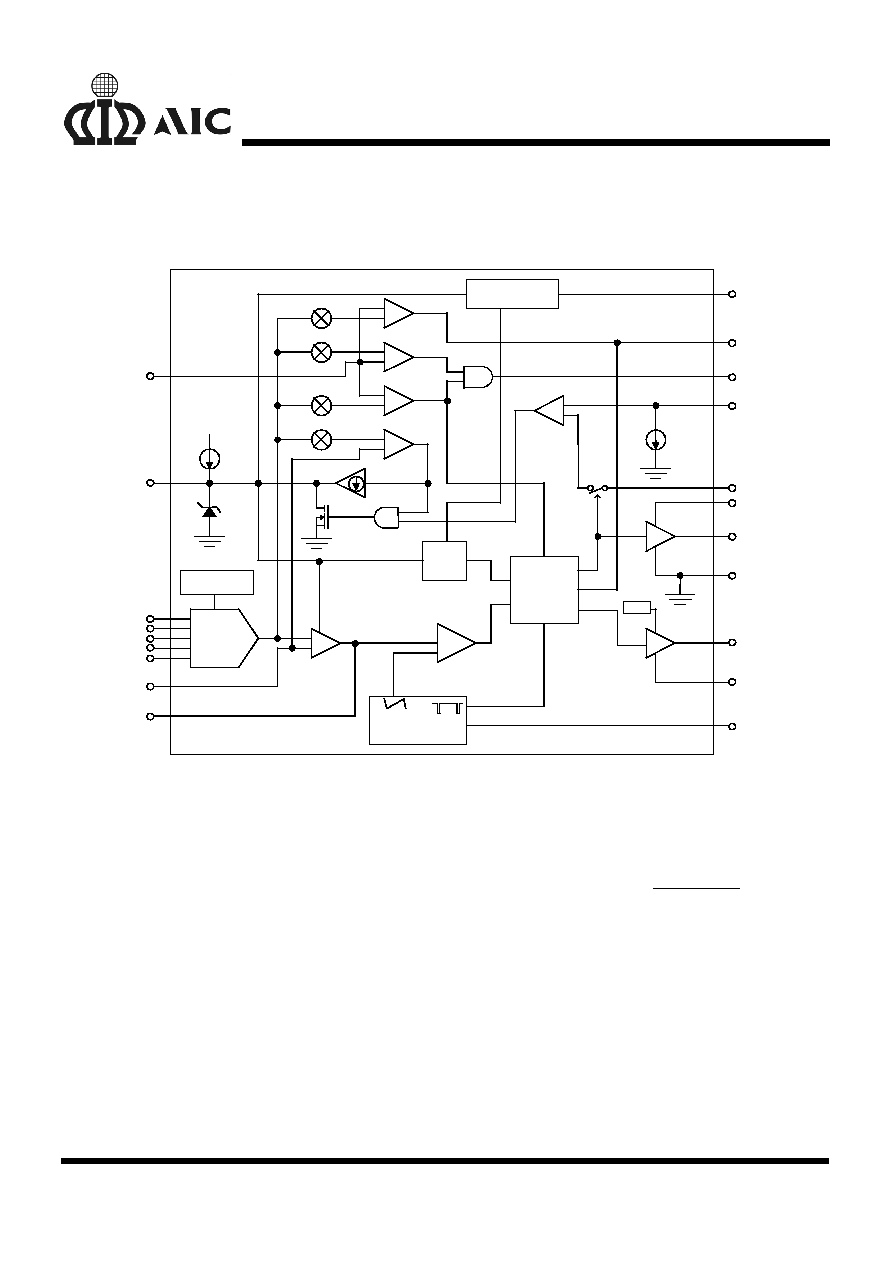
BLOCK DIAGRAM
VCC
GND
LGATE
PGND
RT
BOOT
UGATE
PHASE
OCSET
OVP
PGOOD
VCC
CONTROL
LOGIC
I
OCS
200
µA
OVER
CURRENT
VID0
VID1
VID2
VID3
VID4
VSEN
SOFT
START
10
µA
4V
FB
OVP
POWER-ON
RESET
50%
POWER GOOD
SS
90%
110%
115%
ERROR AMP
OSCILLATOR
COMPARATOR
PWM
REFERENCE
COMP
5-BITS DAC
+
-
+
-
+
-
+
-
+
-
+
-
+
-
VDAC
PIN DESCRIPTIONS
PIN 1: VSEN - Converter output voltage sense
pin. Connect this pin to the
converter output. The PGOOD
and OVP comparator circuits use
this signal to report output voltage
status and perform overvoltage
protection function.
PIN 2:OCSET - Current limit sense pin. Connect a
resistor R
OCSET
from this pin to the
drain of the external MOSFET.
R
OCSET
, an internal 200
µA current
source (I
OCS
), and the external
MOSFET on-resistance (R
DS(ON)
)
jointly set the over current trip
point according to the following
equation:
I
I
R
R
PEAK
OCS
OCSET
DS ON
=
◊
(
)
If FB pin voltage is sensed to be
below 50% of the internal voltage
reference VDAC, the over current
comparator cycles the soft-start
function.
PIN 3:SS
- Soft start pin. Connect a capacitor
from this pin to ground. An internal
10
µA current source provides soft
start function for the converter.