þÿ

AIC1571
5-bit DAC, Synchronous PWM Power
Regulator with Dual Linear Controllers
Analog Integrations Corporation 4F, 9 Industry E. 9th Rd, Science-Based Industrial Park, Hsinchu, Taiwan
DS-1571-00 012102
TEL: 886-3-5772500
FAX: 886-3-5772510
www.analog.com.tw
1
n
FEATURES
l
Provides 3 Regulated Voltages for Microprocessor
Core, Clock and GTL Power.
l
Simple Voltage-Mode PWM Control.
l
Dual N-Channel MOSFET Synchronous Driver.
l
Operates from +3.3V, +5V and +12V Inputs.
l
Fast Transient Response.
l
Full 0% to 100% Duty Ratios.
l
±1.0% Output Voltage for VCORE and
±
2.0%
Output Voltage Reference for VCLK and VGTL.
l
TTL Compatible 5-bit Digital-to-Analog Core Output
Voltage Selection. Range from 1.3V to 3.5V.
0.1V Steps from 2.1V to 3.5V.
0.05V Steps from 1.3V to 2.05V.
l
Adjustable Current Limit without External Sense
Resistor.
l
Microprocessor Core Voltage Protection against
Shorted MOSFET.
l
Power Good Output Voltage Monitor.
l
Over-Voltage and Over-Current Fault Monitors.
l
200KHz Free-Running Oscillator Programmable up
to 350KHz.
n
APPLICATIONS
l
Full Motherboard Power Regulation for Computers.
l
Power Integrations for 3 Output Power System.
n
DESCRIPTION
The AIC1571 combines a synchronous voltage mode
controller with two linear controllers as well as the
monitoring and protection functions in this chip. The
PWM controller regulates the microprocessor core
voltage with a synchronous rectified buck converter.
One linear controller regulates power for the GTL
bus and the other linear controller provides power for
the clock driver circuit or memory (1.8V)
An integrated 5 bit D/A converter that adjusts the
core PWM output voltage from 2.1V to 3.5V in 0.1V
increments and from 1.3V to 2.05V in 0.05V incre-
ments. The linear regulator uses an internal driver
device to provide 2.5V±2.5%. The linear controller
drives with an external N-channel MOSEFET to pro-
vide 1.5V±2.5%.
This chip monitors all the output voltages. Power
Good signal is issued when the core voltage is
within ±10% of the DAC setting and the other levels
are above their under-voltage levels. Over-voltage
protection for the core output uses the lower N-
channel MOSFET to prevent output voltage above
115% of the DAC setting.
The PWM over-current function monitors the output
current by using the voltage drop across the upper
MOSFET's R
DS(on)
, eliminating the need for a current
sensing resistor
.
AIC1571
2
n
ORDERING INFORMATION
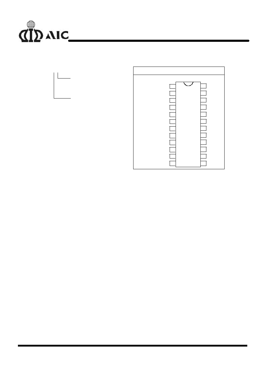
PIN CONFIGURATION
PACKING TYPE
TR: TAPE & REEL
TB: TUBE
PACKAGING TYPE
S: SMALL OUTLINE
AIC1571CXXX
Example: AIC1571CSTR
à
in SO-24 Package & Taping &
Reel Packing Type
SO-24
TOP VIEW
LGATE
UGATE
PHASE
VSEN
PGND
OCSET
16
15
FB1
GATE3
COMP1
FB3
24
22
23
21
20
19
17
18
14
13 GATE2
GND
1
3
4
2
5
7
6
8
9
10
VID0
VID4
VID3
VID2
VCC
VID1
RT
PGOOD
SS
FAULT
11
12
VIN2
FB2
n
ABSOLUTE MAXIMUM RATINGS
Supply Voltage, V
CC
.................. ... ... ... ... ........ ... ... ... ............ ..... ... ..................... +15V
PGOOD, FAULT and GATE Voltage
........ ... ........ ... ... ..... .... GND -0.3V to V
CC
+0.3V
Input, Output , or I/O Voltage
......... ...... ... ... ... ... ... ... ... ..... ... ............ GND -0.3V to 7V
Recommended Operating Conditions
Supply Voltage; VCC
... ... .................. ................... +12V±10%
Ambient temperature Range
... ... ..... ... ... ... ... ................. 0
°
C~70
°
C
Junction Temperature Range
... ... ......... ... ... .................. 0
°
C~100
°
C
Thermal Information
Thermal Resistance,
JA
SOIC package
... ... ... ... ... ... ... ... ... ... ... ... ... ..... ............... 100
°
C/W
SOIC package (with 3in
2
of copper)
... ...... ... ... .......... ......... 90
°
C/W
Maximum Junction Temperature (Plastic Package)
... ... ... ... ... ... ..... ... ...... 150
°
C
Maximum Storage Temperature Range
... ... ... ... ... ... ... ... ... ... ... .... -65
°
C ~ 150
°
C
Maximum Lead Temperature (Soldering 10 sec)
... ... ... ... ... ... ... ... ... ..... ... 300
°
C
n
TEST CIRCUIT
Refer to APPLICATION CIRCUIT.
AIC1571
3
n
ELECTRICAL CHARACTERISTICS
(V
cc
=12V, T
J
=25
°
C, Unless otherwise
specified)
PARAMETER
TEST CONDITIONS
SYMBOL MIN.
TYP.
MAX.
UNIT
VCC SUPPLY CURRENT
Supply Current
UGATE, LGATE, GATE2
and GATE3 open
I
CC
1.8
5
mA
POWER ON RESET
Rising VCC Threshold
V
OCSET
=4.5V
VCC
THR
8.6
9.5
10.4
V
Falling VCC Threshold
V
OCSET
=4.5V
VCC
THF
8.2
9.2
10.2
V
Rising VIN2 Under-Voltage
Threshold
VIN2
THR
2.5
2.6
2.7
V
VIN2 Under-Voltage Hystere-
sis
VIN2
HYS
130
mV
Rising V
OCSET1
Threshold
V
OCSETH
1.3
V
OSCILLATOR
Free Running Frequency
RT=Open
F
170
200
230
KHz
Ramp. Amplitude
RT=open
V
OSC
1.3
V
P-P
REFERENCE AND DAC
DAC (VID0~VID4) Input Low
Voltage
VID
L
0.8
V
DAC (VID0~VID4) Input High
Voltage
VID
H
2
V
DACOUT Voltage Accuracy
VDAC=1.3V~3.5V
-1.0
+1.0
%
FB2 Reference Voltage
V
REF2
1.245
1.270
1.295
V
FB3 Reference Voltage
V
REF3
1.250
1.275
1.300
V
AIC1571
4
n
ELECTRICAL CHARACTERISTICS
(Continued)
PARAMETER
TEST CONDITIONS
SYMBOL
MIN.
TYP.
MAX.
UNIT
LINEAR CONTROLLER
Regulation
0 < I
GATE2/3
< 10mA
-2.5
+2.5
%
Under-Voltage Level
FB2/3 falling
FB2/3
UV
70
80
%
PWM CONTROLLER ERROR AMPLIFIER
DC GAIN
76
dB
Gain Bandwidth Product
GBWP
11
MHz
Slew Rate
COMP1=10pF
SR
6
V/
µ
S
PWM CONTROLLER GATE DRIVER
Upper Drive Source
VCC=12V, V
UGATE
=11V
R
UGH
5.2
6.5
Upper Drive Sink
VCC=12V, V
UGATE
=1V
R
UGL
3.3
5
Lower Drive Source
VCC=12V, V
LGATE
=11V
R
LGH
4.1
6
Lower Drive Sink
VCC=12V, V
LGATE
=1V
R
LGL
3
5
PROTECTION
V
OUT1
Voltage Over-Voltage
Trip
VSEN Rising
OVP
112
115
118
%
OCSET Current Source
V
OCSET
=4.5V
DC
I
OCSET
170
200
230
µ
A
FAULT Sourcing Current
V
FAULT
=10V
I
OVP
10
16
mA
Soft-Start Current
I
SS
11
µ
A
Chip Shutdown Soft Start
Threshold
1.0
V
POWER GOOD
V
OUT1
Upper Threshold
VSEN Rising
109
110.5
112
%
V
OUT1
Under-Voltage
VSEN Falling
90.5
92
93.5
%
V
OUT1
Hysteresis
(VSEN/DACOUT)
Upper and Lower Thresh-
old
3
%
P
GOOD
Voltage Low
I
PGOOD
=-4mA
V
PGOOD
0.5
V
AIC1571
5
n
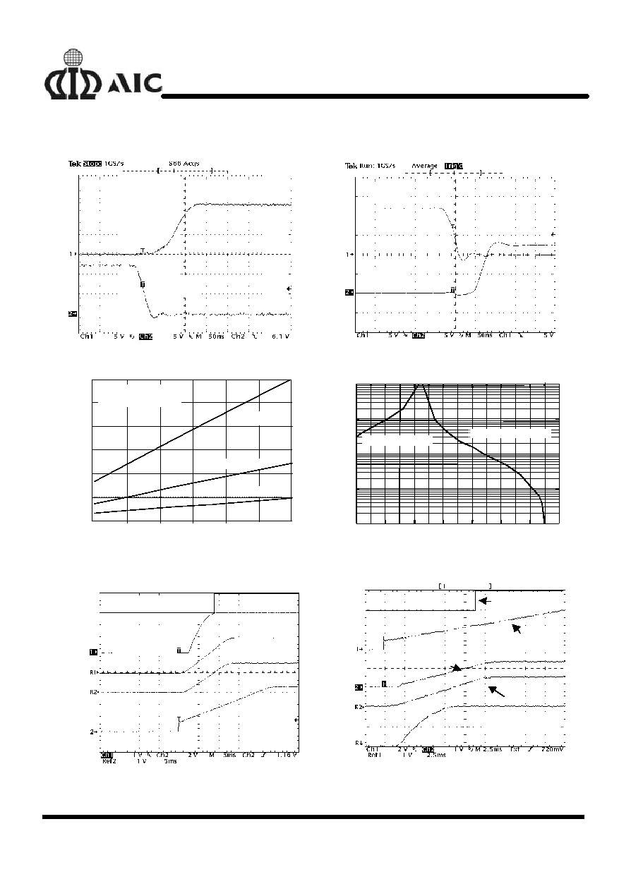
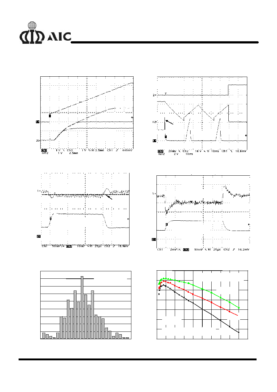
TYPICAL PERFORMANCE CHARACTERISTICS
U
GATE
L
GATE
U
GATE
L
GATE
FIG.1 The gate drive waveforms
I
CC
(
mA)
Switching Frequency (KHz)
100
150
200
250
300
350
400
0
10
20
30
40
50
60
C
UGATE
=C
LGATE
=C
GATE
V
CC
=12V
C
GATE
=5000pF
C
GATE
=2000pF
C
GATE
=660pF
100
150
200
250
300
350
400
1
10
100
1000
10000
Resistance (k
)
Switching Frequency (KHz)
R
T
Pull Down to GND
R
T
Pull Up to +12V
450
FIG. 2 Bias Supply Current VS. Frequency FIG. 3 R
T
Resistance VS. Frequency
V
OUT2
(1V/div)
SS (2V/div)
V
OUT3
(1V/div)
V
OUT1
(1V/div)
PGOOD (5V/div)
SS (2V/div)
V
OUT1
(1V/div)
V
OUT3
SS (2V/div)
PGOOD (5V/div)
V
OUT1
(1V/div)
SS (2V/div)
V
OUT3
V
OUT2
(1V/div)
PGOOD (5V/div)
FIG.4-1 Circuit 1---Soft Start Interval
with 3 Outputs FIG.4-2 Circuit 2---Soft Start Interval
with 3
and PGOOD
Outputs and PGOOD
AIC1571
6
n
TYPICAL PERFORMANCE CHARACTERISTICS
(Continued)
VDAC=3.5V
VDAC=1.3V
VDAC=2V
SS
FAULT
SS
10A/div
Inductor Current
Over Load
Applied
FIG. 5 Soft Start Initiates PWM Output
FIG. 6 Over-Current Operation on Inductor
V
OUT1
5A to 12A Load Step
2.0V
DC
V
OUT3
(
2mV/div
)
1A to 2A Load Step
FIG. 7 Transient Response of PWM Output
FIG. 8 Transient Response of Linear Controller
-0.5 -0.4 -0.3 -0.2 -0.1 0.0 0.1 0.2 0.3 0.4 0.5 0.6 0.7
0
10
20
30
40
50
60
70
80
90
Number of Parts
DACOUT=2.0V
TA=25
°
C
0
2
4
6
8
10
12
14
16
18
20
65
70
75
80
85
90
95
100
Power MOSFET : CEB6030L
Vo=2.8V
Vo=2V
Vo=1.3V
V
IN
=5V
Switching Frequency = 200KHz
Efficiency (%)
FIG. 9 DACOUT Voltage Accuracy (%)
FIG.10 Efficiency vs. Load Current (A)
AIC1571
7
n
TYPICAL PERFORMANCE CHARACTERISTICS
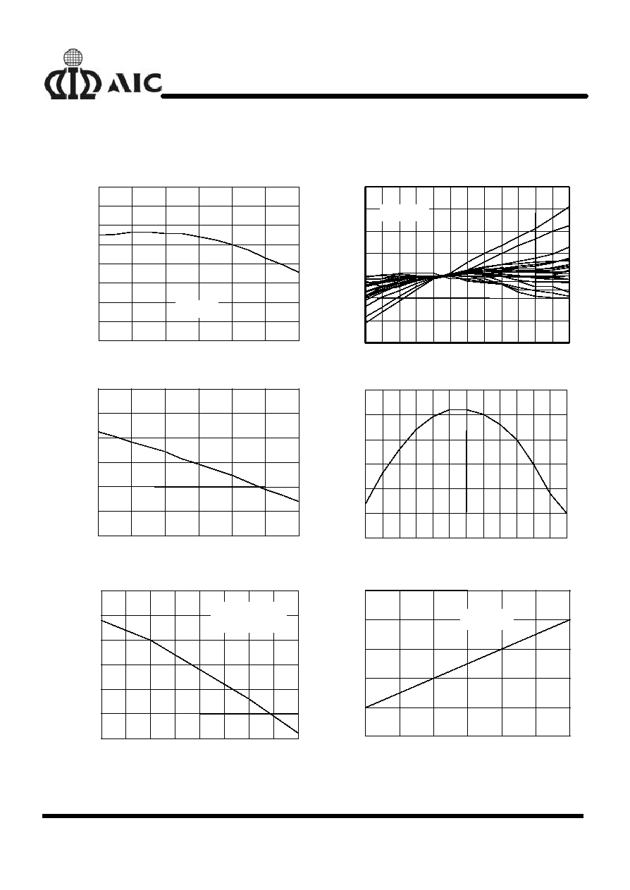
(Continued)
-20
0
20
40
60
80
100
180
185
190
195
200
205
210
215
220
RT=OPEN
Switching Frequency (
KHz)
DACOUT Voltage Drift (%)
-20 -10 0
10
20
30
40
50
60
70
80
90 100
0.0
0.2
0.4
0.6
0.8
DACOUT=2.0V
-0.6
-0.4
-0.2
FIG.11 Oscillator Frequency vs. Temperature (
°
C)
FIG.12 Temperature Drift of 24 Different Parts
-20
0
20
40
60
80
1
00
180
185
190
195
200
205
210
OCSET Current (
µ
A)
-20 -10
0
10
20
30
40
50
60
70
80
90
100
9.25
9.30
9.35
9.40
9.45
9.50
9.55
SS Charge Current (
uA)
FIG.13 OCSET Current vs .Temperature (
°
C)
FIG.14 SS Current vs. Temperature (
°
C)
10
11
12
13
14
15
16
17
18
-2.0
-1.5
-1.0
-0.5
0.0
0.5
1.0
DACOUT=2.0V
V
IN
=5V
NO LOAD
V
CORE
Drift Voltage (mV)
4.0
4.5
5.0
5.5
6.0
6.5
7.0
-0.2
-0.1
0.0
0.1
0.2
0.3
NO LOAD
Vcore Drift (mV)
FIG.15 Vcore Drift vs. VCC (V)
FIG.16 Vcore Drift vs. VIN (V)
AIC1571
8
n
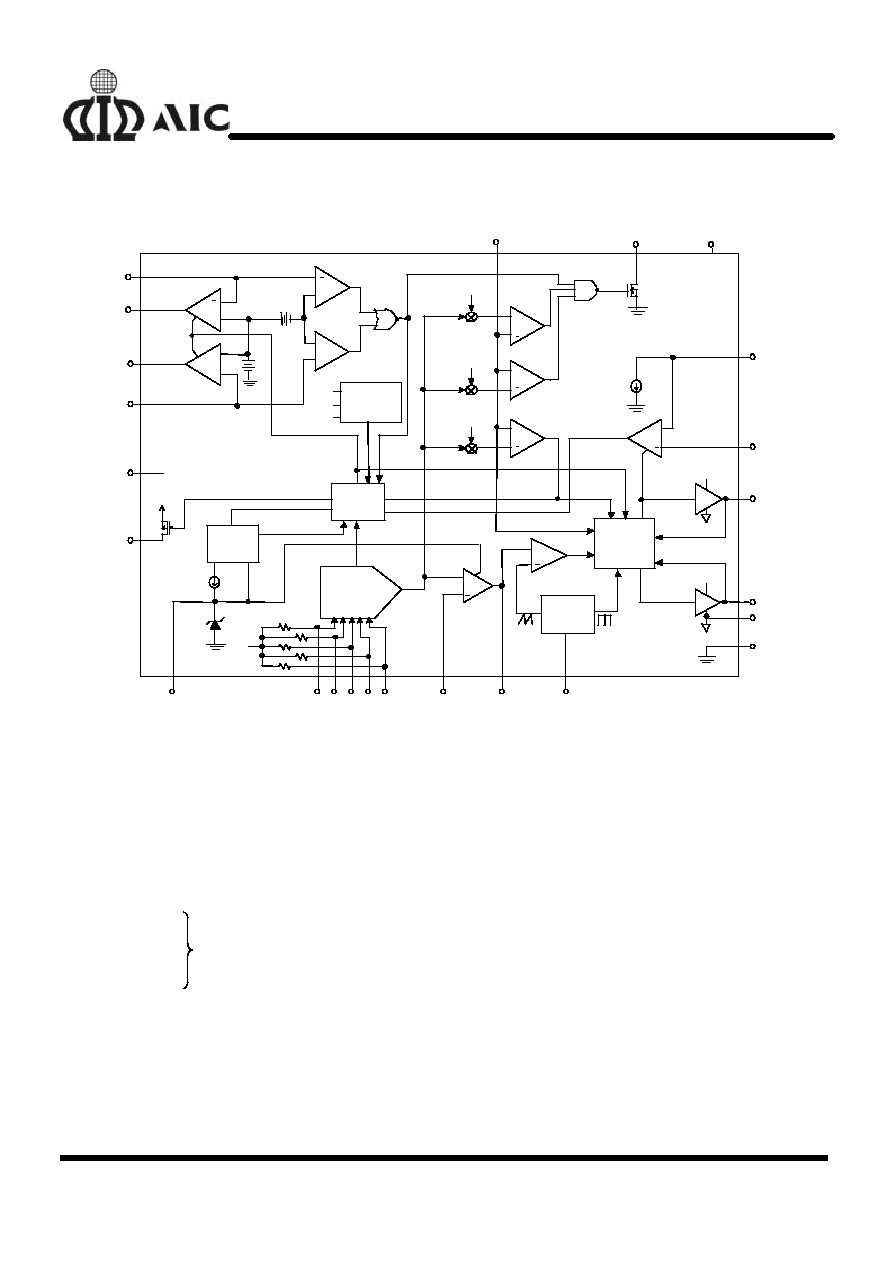
BLOCK DIAGRAM
5 BIT TTL D/A
CONVERTER
(DAC)
+
+
+
+
+
SS
110%
90%
115%
0.3V
1.26V
70K
FB3
FB2
GATE3
FAULT
VIN2
VID4
VID3
VID2
VID1
VID0
SOFT
START
10
µ
A
4V
70K
70K
70K
70K
5V
FB1
COMP1
RT
OCSET
PHASE
GND
PGND
LGATE
UGATE
200
µ
A
GATE CONTROL
VCC
PGOOD
VCC
VCC
OSCILLATOR
PWM COMP
OV
OC1
VSEN
ERROR
AMP
LUV
INHiBIT
VCC
OCSET
VIN2
POWER
ON RESET
OFF
VCC
FAULT
LOGIC &
LATCH
+
+
-
+
+
+
-
GATE2
n
PIN DESCRIPTIONS
Pin 1: VCC:
The chip power supply pin. It also
provides the gate bias charge for
all the MOSFETs controlled by
the IC. Recommended supply
voltage is 12V.
Pin 2:
VID4:
Pin 3: VID3:
Pin 4: VID2:
Pin 5: VID1:
Pin 6: VID0:
5bit DAC voltage select pin. TTL
inputs used to set the internal
voltage reference VDAC. When
left open, these pins are inter-
nally pulled up to 5V and provide
logic ones. The level of VDAC
sets the converter output voltage
as well as the PGOOD and OVP
thresholds.
Table 1 specifies the VDAC volt-
age for the 32 combinations of
DAC inputs.
Pin 7: PGOOD:
Power good indicator pin. PGOOD
is an open drain output. This pin is
pulled low when the converter out-
put is ±10% out of the VDAC ref-
erence voltage and the other out-
puts are below their under-voltage
thresholds. The PGOOD output is
open for VID codes that inhibit op-
eration. See Table 1.
Pin 8: FAULT:
This pin is low during normal op-
eration, but it is pulled to VCC in
the event of an over-voltage or over-
current condition.

AIC1571
9
Pin 9:
SS:
Soft-start pin. Connect a capaci-
tor from this pin to ground. This
capacitor, along with an internal
10
µ
A (typically) current source,
sets the soft-start interval of the
converter.
Pulling this pin low will shut down
the IC.
Pin 10: RT:
Frequency adjustment pin. Con-
necting a resistor (RT) from this
pin to GND, increasing the fre-
quency. Connecting a resistor
(RT) from this pin to VCC, de-
creasing the frequency by the
following figure (Fig.3).
Pin 11: FB2:
Connect this pin to a resistor di-
vider to set the linear controller
output voltage.
Pin 12: VIN2:
This pin is used to monitor the
3.3V supply. If, following a start-
up cycle, the voltage drops below
2.6V (typically), the chip shuts
down. A new soft-start cycle is
initiated upon return of the 3.3V
supply above the under-voltage
threshold.
Pin 13: GATE2: Linear Controller output drive pin.
This pin can drive either a Dar-
lington NPN transistor or a N-
channel MOSFET.
Pin 14: GND:
Signal GND for IC. All voltage
levels are measured with respect
to this pin.
Pin 15: GATE3: Linear Controller output drive pin.
This pin can drive either a Dar-
lington NPN transistor or a N-
channel MOSFET.
Pin 16: FB3:
Negative feedback pin for the
linear controller error amplifier
connect this pin to a resistor di-
vider to set the linear controller
output voltage.
Pin 17: COMP1: External compensation pin. This
pin is connected to error amplifier
output and PWM comparator. An
RC network is connected to FB1
in to compensate the voltage
control feedback loop of the con-
verter.
Pin 18: FB1:
The error amplifier inverting input
pin. the FB1 pin and COMP1 pin
are used to compensate the volt-
age-control feedback loop.
Pin 19: VSEN:
Converter output voltage sense
pin. Connect this pin to the con-
verter output. The PGOOD and
OVP comparator circuits use this
signal to report output voltage
status and for over-voltage protec-
tion function.
Pin 20: OCSET: Current limit sense pin. Connect
a resistor R
OCSET
from this pin to
the drain of the external high-side
N-MOSFET. R
OCSET
, an internal
200
µ
A current source (I
OCSET
),
and the upper N-MOSFET on-
resistance (R
DS(ON)
) set the over-
current trip point according to the
following equation:
I
I
R
R
PEAK
OCSET
OCSET
DS(ON)
=
×
Pin 21: PGND:
Driver power GND pin. PGND
should be connected to a low im-
pedance ground plane in close to
lower N-MOSFET source.
Pin 22: LGATE: Lower N-MOSFET gate drive pin.
Pin 23: PHASE: Over-current detection pin. Con-
nect the PHASE pin to source of
the external high-side N-
MOSFET. This pin detects the
voltage drop across the high-side
N-MOSFET R
DS(ON)
for over-
current protection.
Pin 24: UGATE: External high-side N-MOSFET
gate drive pin. Connect UGATE
to gate of the external high-side
N-MOSFET.

AIC1571
10
n
APPLICATIONS INFORMATION
The AIC1571 is designed for microprocessor
computer applications with 3.3V and 5V power,
and 12V bias input. This IC has one PWM con-
troller and two linear controllers. The PWM con-
troller is designed to regulate the microproces-
sor core voltage (V
OUT1
) by driving 2 MOSFETs
(Q1 and Q2) in a synchronous rectified buck
converter configuration. The core voltage is
regulated to a level programmed by the 5 bit D/A
converter. One integrated linear controller sup-
plies the 2.5V clock power (V
OUT2
). The other
linear controller drive an external MOSFET(Q3)
to supply the GTL bus power(V
OUT3
)
The Power-On Reset (POR) function continually
monitors the input supply voltage +12V at VCC
pin, the 5V input voltage at OCSET pin, and the
3.3V input at VIN2 pin. The POR function initi-
ates soft-start operation after all three input sup-
ply voltage exceed their POR thresholds.
Soft-Start
The POR function initiates the soft-start se-
quence. Initially, the voltage on SS pin rapidly
increases to approximate 1V. Then an internal
10µA current source charges an external ca-
pacitor (C
SS
) on the SS pin to 4V. As the SS pin
voltage slews from 1V to 4V, the PWM error
amplifier reference input (Non-inverting terminal)
and output (COMP1 pin) is clamped to a level
proportional to the SS pin voltage. As the SS pin
voltage slew from 1V to 4V, the output clamp
generates PHASE pulses of increasing width
that charge the output capacitors. Additionally
both linear regulator's reference inputs are
clamped to a voltage proportional to the SS pin
voltage. This method provides a controlled out-
put voltage smooth rise.
Fig.4 and Fig.5 show the soft-start sequence for
the typical application. The internal oscillator's
triangular waveform is compared to the clamped
error amplifier output voltage. As the SS pin volt-
age increases, the pulse width on PHASE pin
increases. The interval of increasing pulse width
continues until output reaches sufficient voltage
to transfer control to the input reference clamp.
Each linear output (VOUT2 and VOUT3) initially
follows a ramp. When each output reaches suf-
ficient voltage the input reference clamp slows
the rate of output voltage rise. The PGOOD sig-
nal toggles `high' when all output voltage levels
have exceeded their under-voltage levels.
Fault Protection
All three outputs are monitored and protected
against extreme overload. A sustained overload
on any output or over-voltage on PWM output
disable all converters and drive the FAULT pin to
VCC.
AIC1571
11
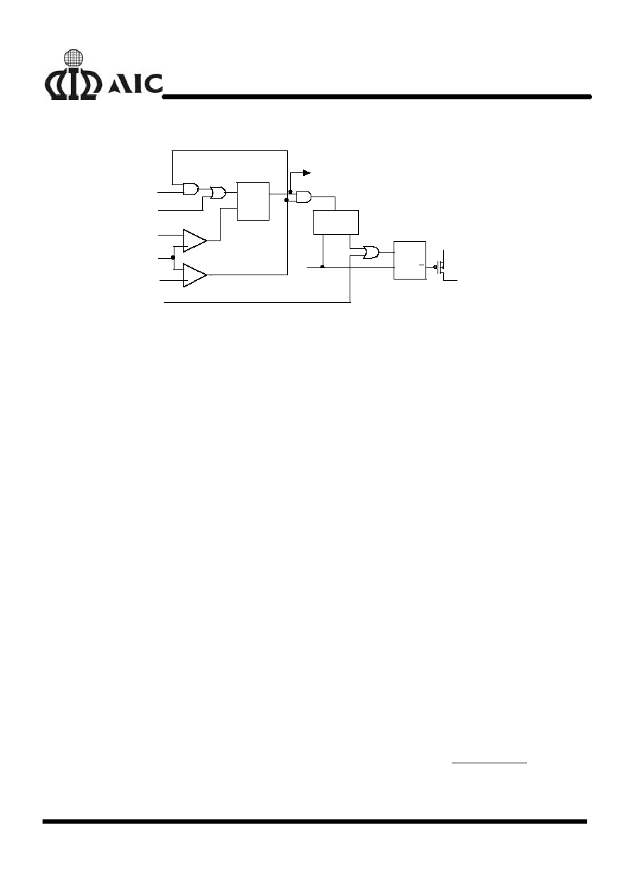
+
+
0.2V
OV
LATCH
OVER CURRENT
3.6V
SS
OC1
R
LUV
Q
S
FAULT
VCC
FAULT LATCH
POR
Q
R
S
R
S
COUNTER
INHIBIT
Fig. 17 Simplified Schematic of Fault Logic
A simplified schematic is shown in figure 17. An
over-voltage detected on VSEN immediately sets
the fault latch. A sequence of three over-current
fault signals also sets the fault latch. An under-
voltage event on either linear output (FB2 or FB3)
is ignored until the soft-start interval. Cycling the
bias input voltage (+12V) off then on reset the
counter and the fault latch.
Over-Voltage Protection
During operation, a short on the upper PWM
MOSFET (Q1) causes V
OUT1
to increase. When
the output exceed the over-voltage threshold of
115% of DACOUT, the FAULT pin is set to fault
latch and turns Q2 on as required in order to
regulate V
OUT1
to 115% of DACOUT. The fault
latch raises the FAULT pin close to VCC potential.
A separate over-voltage circuit provides protection
during the initial application of power. For voltage
on VCC pin below the power-on reset (and above
4V), should VSEN exceed 0.7V, the lower
MOSFET (Q2) is driven on as needed to regulate
V
OUT1
to 0.7V.
Over-Current Protection
All outputs are protected against excessive over-
current. The PWM controller uses upper
MOSFET's on-resistance, R
DS(ON)
to monitor the
current for protection against shorted outputs.
Both the linear regulator and controller monitor
FB2 and FB3 for under-voltage to protect against
excessive current.
When the voltage across Q1 (I
D
·
R
DS(ON)
) exceeds
the level (200
µ
A
·
R
OCSET
), this signal inhibit all
outputs. Discharge soft-start capacitor (Css) with
10
µ
A current sink, and increments the counter.
Css recharges and initiates a soft-start cycle
again until the counter increments to 3. This sets
the fault latch to disable all outputs. Fig. 6 illus-
trates the over-current protection until an over load
on OUT1.
Should excessive current cause FB2 or FB3 to fall
below the linear under-voltage threshold, the LUV
signal sets the over-current latch if Css is fully
charged. Cycling the bias input power off then on
reset the counter and the fault latch.
The over-current function for PWM controller will
trip at a peak inductor current (I
PEAK
) determined
by:
I
I
R
R
PEAK
OCSET
OCSET
DS(ON)
=
×
The OC trip point varies with MOSFET's tempera-
AIC1571
12
ture. To avoid over-current tripping in the normal
operating load range, determine the R
OCSET
resis-
tor from the equation above with:
1. The maximum R
DS(ON)
at the highest junction.
2. The minimum I
OCSE
T
from the specification ta-
ble.
3. Determine I
PEAK
> I
OUT(MAX)
+ (inductor ripple
current) /2.
PWM OUT1 Voltage Program
The output voltage of the PWM converter is pro-
grammed to discrete levels between 1.3V to 3.5V.
The VID pins program an internal voltage reference
(DACOUT) through a TTL compatible 5 bit digital
to analog converter. The VID pins can be left open
for a logic 1 input, because they are internally
pulled up to 5V by a 70k
resistor. Changing the
VID inputs during operation is not recommended.
All VID pin combinations resulting in an INHIBIT
disable the IC and the open collector at the
PGOOD pin.
Shutdown
Holding the SS pin low with an open drain or col-
lector signal turns off all three regulators.
The VID codes resulting in an INHIBIT as shown in
Table 1 also shut down the IC.
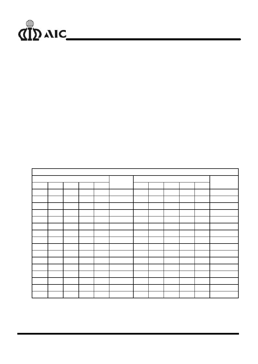
Table 1 V
OUT1
Voltage Program (0=connected to GND, 1=open or connected to 5V)
For all package version
PIN NAME
PIN NAME
VID4
VID3
VID2
VID1
VID0
DACOUT
VOLTAGE
VID4
VID3
VID2
VID1
VID0
DACOUT
VOLTAGE
0
1
1
1
1
1.30V
1
1
1
1
1
INHIBIT
0
1
1
1
0
1.35V
1
1
1
1
0
2.1 V
0
1
1
0
1
1.40V
1
1
1
0
1
2.2 V
0
1
1
0
0
1.45V
1
1
1
0
0
2.3 V
0
1
0
1
1
1.50V
1
1
0
1
1
2.4 V
0
1
0
1
0
1.55V
1
1
0
1
0
2.5 V
0
1
0
0
1
1.60V
1
1
0
0
1
2.6 V
0
1
0
0
0
1.65V
1
1
0
0
0
2.7 V
0
0
1
1
1
1.70V
1
0
1
1
1
2.8 V
0
0
1
1
0
1.75V
1
0
1
1
0
2.9 V
0
0
1
0
1
1.80 V
1
0
1
0
1
3.0 V
0
0
1
0
0
1.85 V
1
0
1
0
0
3.1 V
0
0
0
1
1
1.90 V
1
0
0
1
1
3.2 V
0
0
0
1
0
1.95 V
1
0
0
1
0
3.3 V
0
0
0
0
1
2.00 V
1
0
0
0
1
3.4 V
0
0
0
0
0
2.05 V
1
0
0
0
0
3.5 V
AIC1571
13
Layout Considerations
Any inductance in the switched current path
generates a large voltage spike during the
switching interval. The voltage spikes can de-
grade efficiency, radiate noise into the circuit,
and lead to device over-voltage stress. Careful
component selection and tight layout of critical
components, and short, wide metal trace mini-
mize the voltage spike.
1) A ground plane should be used. Locate the
input capacitors (C
IN
) close to the power
switches. Minimize the loop formed by C
IN
,
the upper MOSFET (Q1) and the lower
MOSFET (Q2) as possible. Connections
should be as wide as short as possible to
minimize loop inductance.
2) The connection between Q1, Q2 and output
inductor should be as wide as short as prac-
tical. Since this connection has fast voltage
transitions will easily induce EMI.
3) The output capacitor (C
OUT
) should be locat-
ed as close the load as possible. Because
minimize the transient load magnitude for
high slew rate requires low inductance and
resistance in circuit board
4) The AIC1571 is best placed over a quiet
ground plane area. The GND pin should be
connected to the groundside of the output
capacitors. Under no circumstances should
GND be returned to a ground inside the C
IN
,
Q1, Q2 loop. The GND and PGND pins
should be shorted right at the IC. This help
to minimize internal ground disturbances in
the IC and prevents differences in ground
potential from disrupting internal circuit op-
eration.
5) The wiring traces from the control IC to the
MOSFET gate and source should be sized
to carry 1A current. Locate C
OUT2
close to
the AIC1571 IC.
6) The Vcc pin should be decoupled directly to
GND by a 1uF ceramic capacitor, trace
lengths should be as short as possible.
+
+
+
V
OUT
C
OUT
Q1
+3.3V
IN
+5V
IN
L
OUT
GATE3
C
IN
Q2
C s s
SS
GATE2
PGND
LGATE
PHASE
UGATE
OCSET
VIN2
GND
VCC
+12V
+
+
Q3
V
OUT3
C
OUT3
Power Plane Layer
Circuit Plane Layer
Via
Connection
to
Ground
Plane
+
Q4
V
OUT2
C
OUT2
Fig. 18 Printed circuit board power planes and islands

AIC1571
14
A multi-layer printed circuit board is recom-
mended. Figure 18 shows the connections of
the critical components in the converter. The C
IN
and C
OUT
could each represent numerous physi-
cal capacitors. Dedicate one solid layer for a
ground plane and make all critical component
ground connections with vias to this layer.
PWM Output Capacitors
The load transient for the microprocessor core
requires high quality capacitors to supply the
high slew rate (di/dt) current demand.
The ESR (equivalent series resistance) and ESL
(equivalent series inductance) parameters rather
than actual capacitance determine the buck ca-
pacitor values. For a given transient load magni-
tude, the output voltage transient change due to
the output capacitor can be note by the following
equation:
V
ESR
I
ESL
I
T
OUT
OUT
OUT
=
×
+
×
, where
I
OUT
is transient load current step.
After the initial transient, the ESL dependent
term drops off. Because the strong relationship
between output capacitor ESR and output load
transient, the output capacitor is usually chosen
for ESR, not for capacitance value. A capacitor
with suitable ESR will usually have a larger ca-
pacitance value than is needed for energy stor-
age.
A common way to lower ESR and raise ripple
current capability is to parallel several capaci-
tors. In most case, multiple electrolytic capaci-
tors of small case size are better than a single
large case capacitor.
Output Inductor Selection
Inductor value and type should be chosen based
on output slew rate requirement, output ripple
requirement and expected peak current. Inductor
value is primarily controlled by the required cur-
rent response time. The AIC1571 will provide ei-
ther 0% or 100% duty cycle in response to a
load transient. The response time to a transient
is different for the application of load and remove
of load.
t
L
I
V
V
RISE
OUT
IN
OUT
=
×
-
,
t
=
L
I
V
FALL
OUT
OUT
×
.
Where
I
OUT
is transient load current step.
In a typical 5V input, 2V output application, a
3
µ
H inductor has a 1A/
µ
S rise time, resulting in
a 5
µ
S delay in responding to a 5A load current
step. To optimize performance, different combi-
nations of input and output voltage and expected
loads may require different inductor value. A
smaller value of inductor will improve the tran-
sient response at the expense of increase out-
put ripple voltage and inductor core saturation
rating.
Peak current in the inductor will be equal to the
maximum output load current plus half of induc-
tor ripple current. The ripple current is approxi-
mately equal to:
I
=
(V
V
) V
L V
RIPPLE
IN
OUT
OUT
IN
-
×
× ×
f
;
f = AIC1571 oscillator frequency.
The inductor must be able to withstand peak
current without saturation, and the copper resis-
tance in the winding should be kept as low as
possible to minimize resistive power loss
Input Capacitor Selection
Most of the input supply current is supplied by
the input bypass capacitor, the resulting RMS
current flow in the input capacitor will heat it up.
Use a mix of input bulk capacitors to control the
voltage overshoot across the upper MOSFET.
The ceramic capacitance for the high frequency
AIC1571
15
decoupling should be placed very close to the
upper MOSFET to suppress the voltage induced
in the parasitic circuit impedance. The buck ca-
pacitors to supply the RMS current is approxi-
mate equal to:
I
(1 D)
D
I
1
12
V
D
f L
RMS
2
OUT
IN
2
= -
×
×
+
×
×
×
, where
D
V
V
OUT
IN
=
The capacitor voltage rating should be at least
1.25 times greater than the maximum input volt-
age.
PWM MOSFET Selection
In high current PWM application, the MOSFET
power dissipation, package type and heatsink
are the dominant design factors. The conduction
loss is the only component of power dissipation
for the lower MOSFET, since it turns on into
near zero voltage. The upper MOSFET has con-
duction loss and switching loss. The gate char-
ge losses are proportional to the switching fre-
quency and are dissipated by the AIC1571.
However, the gate charge increases the switch-
ing interval, t
SW
which increase the upper MOS-
FET switching losses. Ensure that both MOS-
FETs are within their maximum junction tem-
perature at high ambient temperature by calcu-
lating the temperature rise according to package
thermal resistance specifications.
2
f
t
V
I
D
R
I
P
SW
IN
OUT
DS(ON)
2
OUT
UPPER
×
×
×
+
×
×
=
P
I
R
D)
LOWER
OUT
2
DS(ON)
=
×
× -
(1
The equations above do not model power loss
due to the reverse recovery of the lower
MOSFET's body diode.
The R
DS(ON)
is different for the two previous
equations even if the type devices is used for
both. This is because the gate drive applied to
the upper MOSFET is different than the lower
MOSFET. Logic level MOSFETs should be se-
lected based on on-resistance considerations,
R
DS(ON)
should be chosen base on input and
output voltage, allowable power dissipation and
maximum required output current. Power dissi-
pation should be calculated based primarily on
required efficiency or allowable thermal dissipa-
tion.
Rectifier Schottky diode is a clamp that prevent
the loss parasitic MOSFET body diode from
conducting during the dead time between the
turn off of the lower MOSFET and the turn on of
the upper MOSFET. The diode's rated reverse
breakdown voltage must be greater than twice
the maximum input voltage.
Linear Controller MOSFET Selection
The power dissipated in a linear regulator is :
)
V
(V
I
P
OUT
IN2
OUT
LINEAR
-
×
=
Select a package and heatsink that maintains
junction temperature below the maximum rating
while operation at the highest expected ambient
temperature.
Linear Output Capacitor
The output capacitors for the linear controller
provide dynamic load current. The linear con-
troller uses dominant pole compensation inte-
grated in the error amplifier and is insensitive to
output capacitor selection. C
OUT2
and C
OUT3
should be selected for transient load regulation.
AIC1571
16
n
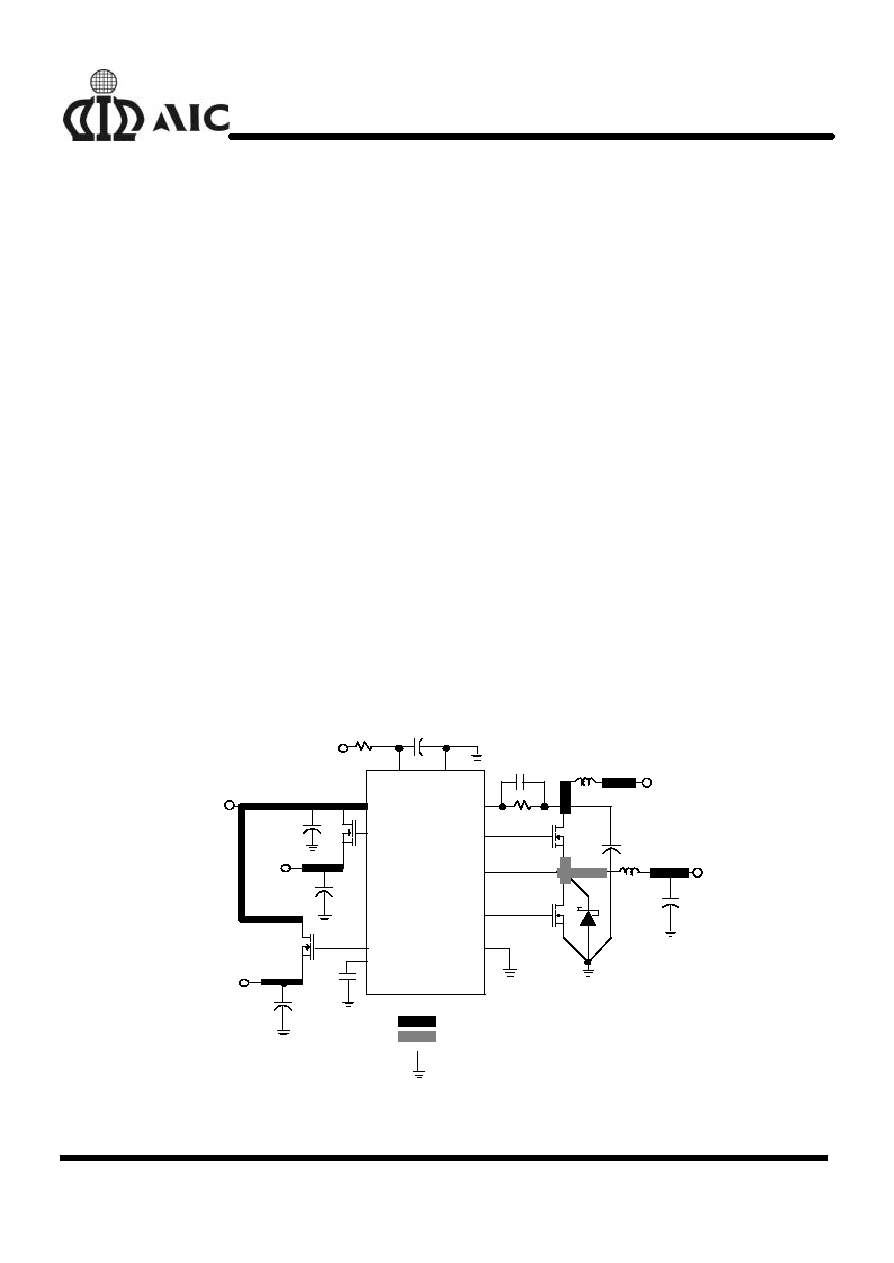
APPLICATION CIRCUIT
+
+
+
+
UGATE
PHASE
VIN2
LGATE
GATE3
PGND
FB3
VSEN
FB1
GATE2
FB2
COMP1
VID0
RT
VID1
FAULT
VID2
PGOOD
VID3
SS
VID4
4 x 1000
µ
F
C45-46
2
3
4
5
6
40nF
C48
9
8
10
7
11
13
Q4
20N03HL
VOUT2
C47-48
1.8V
10K
R12
R11
4.2K
2 x 1000
µ
F
+3.3V
IN
20N03HL
Q3
R12
R11
12
15
16
1.5V
V
OUT3
10K
1.87K
2.2
µ
F
GND
+5V
IN
VCC
+12V
IN
10
R15
C42
2.2nF
D5820
21
1
µ
H
L1
C1-C7
C15
1
µ
F
6 x 1000
µ
F
C18
1000pF
2.2K
R2
C16
Q2
Q1
C24-36
C40
19
C41
R10
0.68
µ
F
160K
10pF
5K
2.2K
732K
R9
R8
R4
L2
OCSET
7 x 1000
µ
F
3.5
µ
H
1
17
18
22
23
24
20
14
V
OUT1
Circuit 1 Motherboard Power application Circuit
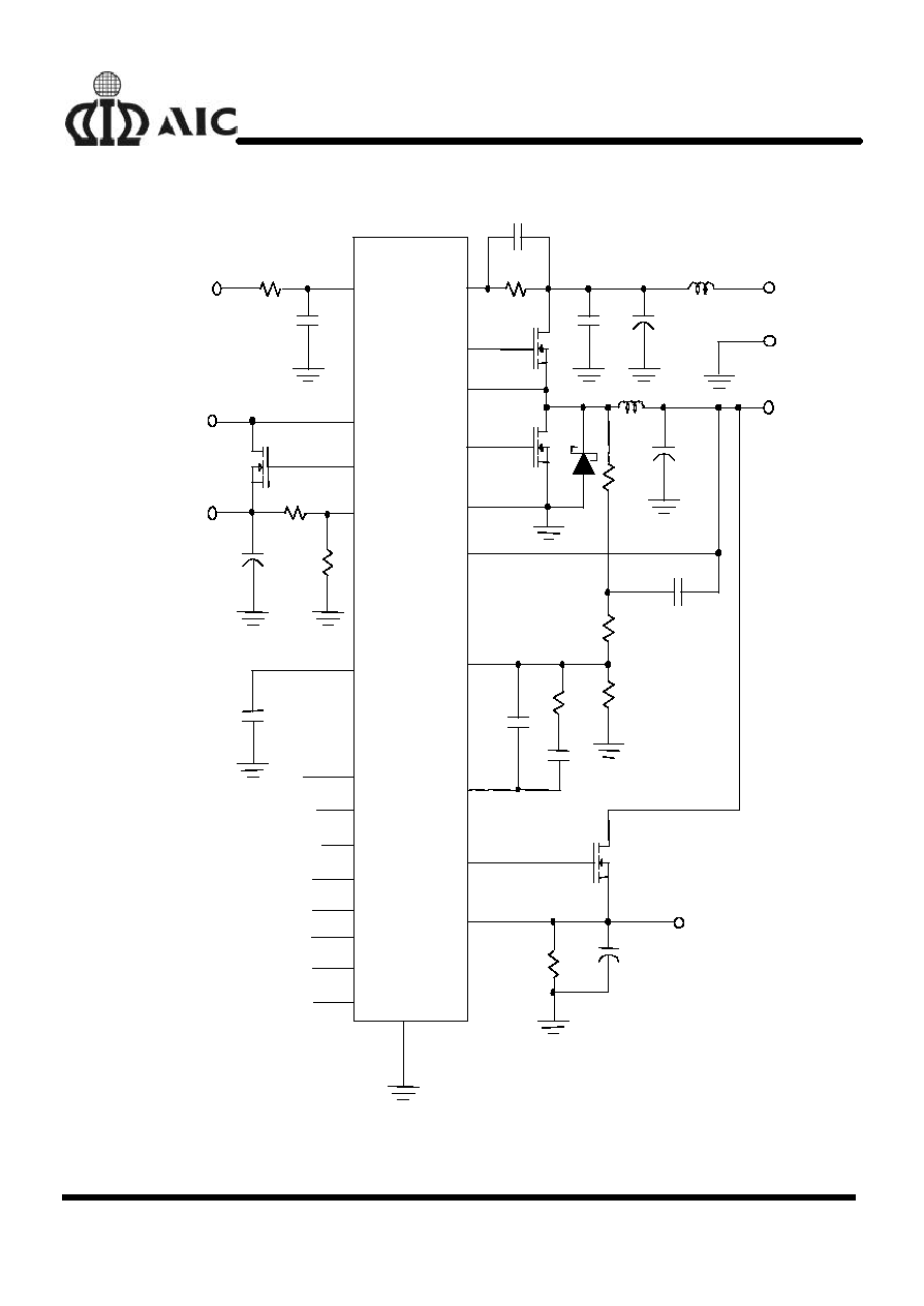
AIC1571
17
+
+
+
+
UGATE
PHASE
VIN2
LGATE
GATE3
PGND
FB3
VSEN
FB1
SS
RT
COMP
1
FAULT
PGOOD
GATE2
VID0
VID1
FB2
VID2
VID3
VID4
20N03H
L
C47
1000
µ
F
Q4
20N03HL
Q3
R14
10K
V
OUT2
1.27V
2.2
µ
F
2 x 1000
µ
F
11
13
40nF
C48
9
8
10
7
2
3
4
5
6
GND
+5V
IN
C43-46
VCC
+12V
IN
10
R15
C42
2.2nF
D5820
21
1
µ
H
L1
C1-C7
6 x1000
µ
F
C15
1
µ
F
C18
1000pF
2.2K
R2
C16
Q2
Q1
C24-36
7 x1000
µ
F
C40
19
C41
R10
R12
R11
0.68
µ
F
160K
10pF
5K
2.2K
732K
R9
R8
R4
L2
OCSET
3.5
µ
H
1
12
15
16
1.5V
VOUT3
+3.3V
IN
10K
1.87K
17
18
22
23
24
20
14
V
OUT1
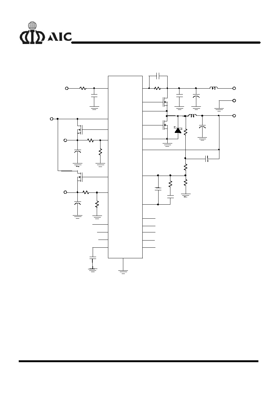
Circuit 2 Power Integration for 3-Output Power System
AIC1571
18
n
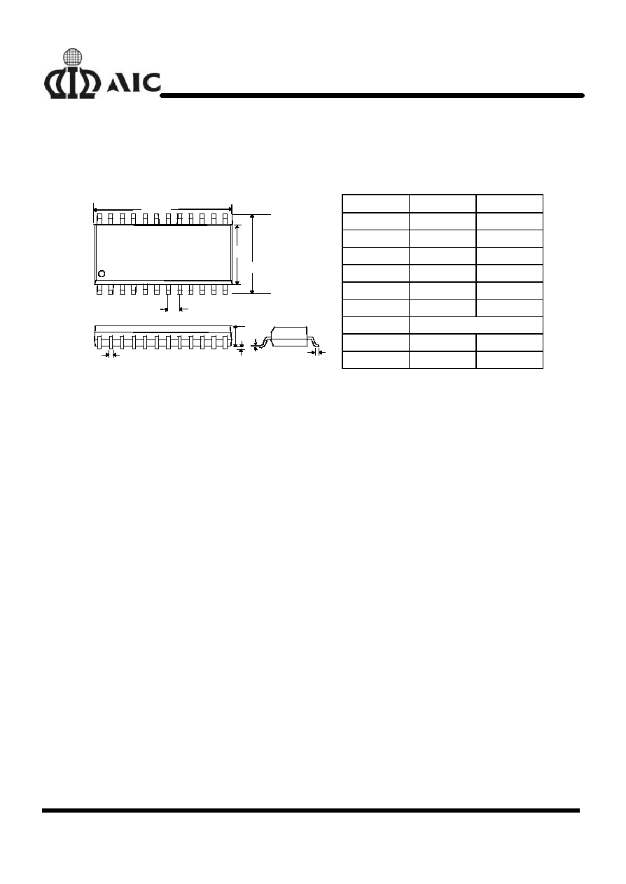
PHYSICAL DIMENSIONS
l
24 LEAD PLASTIC SO (300 mil) (unit: mm)
SYMBOL
MIN
MAX
A
2.35
2.65
A1
0.10
0.30
B
0.33
0.51
C
0.23
0.32
D
15.20
15.60
E
7.40
7.60
e
1.27(TYP)
H
10.00
10.65
e
B
D
A
A1 C
E
H
L
L
0.40
1.27