
AIC1642
3-Pin One-Cell Step-Up DC/DC Converter
Analog Integrations Corporation
4F, 9 Industry E. 9th Rd, Science-Based Industrial Park, Hsinchu, Taiwan
DS-1642-01 012102
TEL: 886-3-5772500
FAX: 886-3-5772510
www.analog.com.tw
1
FEATURES
l
A Guaranteed Start-Up from less than 0.9 V.
l
High Efficiency.
l
Low Quiescent Current.
l
Less Number of External Components needed.
l
Low Ripple and Low Noise.
l
Fixed Output Voltage: 2.7V, 3.0V, 3.3V, and 5V.
l
Space Saving Packages: SOT-89 and TO-92
APPLICATIONS
l
Pagers.
l
Cameras.
l
Wireless Microphones.
l
Pocket Organizers.
l
Battery Backup Suppliers.
l
Portable Instruments.
DESCRIPTION
The AIC1642 is a high efficiency step-up
DC/DC converter for applications using 1 to 4
battery cells. Only three external components
are required to deliver a fixed output voltage of
2.7V, 3.0V, 3.3V, or 5V. The AIC1642 starts up
from less than 0.9V input with 1mA load. Pulse
Frequency Modulation scheme brings optimized
performance for applications with light output
loading and low input voltages. The output rip-
ple and noise are lower compared with the cir-
cuits operating in PSM mode.
The PFM control circuit operating in 100KHz
(max.) switching rate results in smaller passive
components. The space saving SOT-89 and
TO-92 packages make the AIC1642 is an ideal
choice of DC/DC converter for space conscious
applications, like pagers, electronic cameras,
and wireless microphones.
TYPICAL APPLICATION CIRCUIT
D1
GS SS12
VOUT
SW
GND
AIC1642-27
AIC1642-30
AIC1642-33
AIC1642-50
C2
22
µ
F
+
V
OUT
L1
100
µ
H
V
IN
+
C1
47
µ
F
One Cell Step-Up DC/DC Converter

AIC1642
2
ORDERING INFORMATION
TO-92
TOP VIEW
1: GND
2: VOUT
3: SW
1
2
3
1
2
3
SOT-89
TOP VIEW
1: GND
2: VOUT
3: SW
PACKING TYPE
TR: TAPE & REEL
TB: TUBE
BG: BAG
PACKAGE TYPE
X: SOT-89
Z: TO-92
OUTPUT VOLTAGE
27: 2.7V
30: 3.0V
33: 3.3V
50: 5.0V
AIC1642-XXCXXX
Example: AIC1642-27COTR
ý
2.7V Version, in MSOP8 Package
& Tape & Reel Packing Type
PIN CONFIGURATION
ABSOLUATE MAXIMUM RATINGS
Supply Voltage ... ... ... ... ... ... ... ... ... ... ... ... ... ... ... ... ... ... ... ... ... ... ... ... ... ... ... ... ... ... .12V
SW pin Voltage ... ... ... ... ... ... ... ... ... ... ... ... ... ... ... ... ... ... ... ... ... ... ... ... ... ... ... ... ... ... .12V
SW pin Switch Current ... ... ... ... ... ... ... ... ... ... ... ... ... ... ... ... ... ... ... ... ... ... ... ... ... ... ... 0.6A
Operating Temperature Range ... ... ... ... ... ... ... ... ... ... ... ... ..... ... ... ... ... .... .--40
∞
C to 85
∞
C
Storage Temperature Range ... ... ... ... ... ... ... ... ... ... ... ... ... ... ... ... ... ... ... -65
∞
C to 150
∞
C
Lead Temperature (Soldering 10 Sec.) ... ... ... ... ... ... ... ... ... ... ... ... ... ... ... ... ... ... ... 260
∞
C
TEST CIRCUIT
F
OUT
AIC1642
2.5V
VOUT
SW
GND
100
Oscillator Test Circuit

AIC1642
3
n
ELECTRICAL CHARACTERISTICS
(T
A
=25
∞
C, I
OUT
=10mA, Unless otherwise
specified)
PARAMETER
TEST CONDITIONS
SYMBOL
MIN.
TYP.
MAX. UNIT
Output Voltage
V
IN
=1.8V, AIC1642-27
V
IN
=1.8V, AIC1642-30
V
IN
=2.0V, AIC1642-33
V
IN
=3.0V, AIC1642-50
V
OUT
2.633
2.925
3.218
4.875
2.700
3.000
3.300
5.000
2.767
3.075
3.382
5.125
V
Input Voltage
V
IN
8
V
Start-Up Voltage
I
OUT
=1mA, V
IN
:0
2V
V
START
0.8
0.9
V
Hold-on Voltage
I
OUT
=1mA, V
IN
:2
0V
V
HOLD
0.7
V
No-Load Input Current
I
OUT
=0mA
I
IN
15
µ
A
Supply Current
AIC1642-27
AIC1642-30
AIC1642-33
AIC1642-50
V
IN
=V
OUT
x 0.95
Measurement of the IC input
current (VOUT pin)
I
DD1
42
50
60
90
µ
A
Supply Current
V
IN
=V
OUT
+ 0.5V
Measurement of the IC input
current (VOUT pin)
I
DD2
8
µ
A
SW Leakage Current
V
S
W
=10V, V
IN
=V
OUT
+ 0.5V
0.5
µ
A
SW Switch-On Resis-
tance
AIC1642-27
AIC1642-30
AIC1642-33
AIC1642-50
V
IN
=V
SW
x 0.95, V
SW
=0.4V
R
ON
2.2
2.1
2.0
1.9
Oscillator Duty Cycle
V
IN
=V
OUT
x 0.95
Measurement of the SW Pin
Waveform
DUTY
65
75
85
%
Max. Oscillator Freq.
V
IN
=V
OUT
x 0.95
Measurement of the SW Pin
Waveform
F
OSC
80
105
130
KHz
Efficiency
80
%
AIC1642
4
n
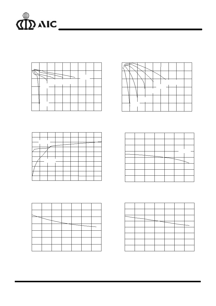
TYPICAL PERFORMANCE CHARACTERISTICS
Capacitor (C1) : 47
µ
F (Tantalum Type)
Diode (D1) : 1N5819 Schottky Type
Fig. 1 AIC1642-27 Load Regulation (L=100
µ
H CD54)
0
20
40
60
80
100
120
140
160
180
2.2
2.3
2.4
2.5
2.6
2.7
2.8
V
IN
=2.0V
V
IN
=1.8V
V
IN
=1.5V
V
IN
=1.2V
V
IN
=0.9V
Output voltage (V)
Output Current (mA)
Fig. 2 AIC1642-27 Efficiency (L=100
µ
H CD54)
0
20
40
60
80
100
120
140
160
180
55
60
65
70
75
80
85
V
IN
=2.0V
V
IN
=1.8V
V
IN
=1.5V
V
IN
=1.2V
V
IN
=0.9V
Efficiency (%)
Output current (mA)
Fig. 3 AIC1642-27 Start-up & Hold-on Voltage (L=100
µ
H)
0
2
4
6
8
10
12
14
16
18
0.0
0.1
0.2
0.3
0.4
0.5
0.6
0.7
0.8
0.9
1.0
Start up
Hold on
Input Voltage (V)
Output Current (mA)
-40
-20
0
20
40
60
80
100
2.62
2.64
2.66
2.68
2.70
2.72
2.74
2.76
2.78
Fig. 4 AIC1642-27 Output Voltage vs. Temperature
No Load
Output Voltage V
OUT
(V)
Temperature (
∞
C)
-
40
-20
0
20
40
60
80
100
20
40
60
80
100
120
140
160
Fig. 5 AIC1642-27 Switching Frequency vs. Temperature
Switching Frequency (kHz)
Temperature (
∞
C)
-40
-20
0
20
40
60
80
100
66
68
70
72
74
76
78
80
82
Fig. 6 AIC1642-27 Maximum Duty Cycle vs. Temperature
Maximum Duty Cycle (%)
Temperature (
∞
C)

AIC1642
5
n
TYPICAL PERFORMANCE CHARACTERISTICS
(Continued)
-40
-20
0
20
40
60
80
100
0.0
0.4
0.8
1.2
1.6
2.0
2.4
2.8
3.2
Fig. 7 AIC1642-27 SW On Resistance vs. Temperature
SW Turn On Resistance (
)
Temperature (
∞
C)
-40
-20
0
20
40
60
80
100
20
24
28
32
36
40
44
48
52
Fig. 8 AIC1642-27 Supply Current IDD1 vs. Temperature
Supply Current IDD1 (
µ
A)
Temperature (
∞
C)
0
10
20
30
40
50
60
70
80
90
100 110 120 130 140
2.0
2.1
2.2
2.3
2.4
2.5
2.6
2.7
2.8
2.9
3.0
3.1
V
IN
=2.0V
V
IN
=.8V
V
IN
=1.5V
V
IN
=1.2V
V
IN
=0.9
Fig. 9 AIC1642-30 Load Regulation (L=100
µ
H CD54)
Output voltage
V
OUT
(V)
Output Current (mA)
0
20
40
60
80
100
120
140
160
180
50
55
60
65
70
75
80
85
V
IN
=2.0V
V
IN
=1.8V
V
IN
=1.5V
V
IN
=1.2V
V
IN
=0.9V
Fig. 10 AIC1642-30 Efficiency (L=100
µ
H CD54)
Efficiency (%)
Output Current (mA)
0
2
4
6
8
10
12
14
16
18
20
0.0
0.1
0.2
0.3
0.4
0.5
0.6
0.7
0.8
0.9
1.0
Fig. 11 AIC1642-30 Start-up & Hold-on Voltage (L=100
µ
H)
Start up
Hold on
Input Voltage (V)
Output Current (mA)
-40
-20
0
20
40
60
80
100
2.90
2.92
2.94
2.96
2.98
3.00
3.02
3.04
3.06
Fig. 12 AIC1642-30 Output Voltage vs. Temperature
No Load
Output
Voltage
Vout (V)
Temperature (
∞
C)