AIC1680
Ultra Low Power Voltage Detector
Analog Integrations Corporation
4F, 9, Industry E. 9th Rd, Science Based Industrial Park, Hsinchu Taiwan, ROC
www.analog.com.tw
DS-1680-00 Dec 29, 00
TEL: 886-3-5772500
FAX: 886-3-5772510
1
FEATURES
Ultra-Low Quiescent Current.
1.5V to 10.0V Input Voltage Operation.
Flexible Detection Voltage Setting
0.1V Step in the Range of 1.6V to 6.0V
High Detection Voltage Accuracy at
±2.5%.
Built-In Detection Voltage Hysteresis.
Three Output Types: N-ch, P-ch and CMOS.
Space Saving Packages: TO-92, SOT-89,
SOT-23 and SOT23-5.
APPLICATIONS
Battery Checker for Battery-Operated Systems.
CPU & Logic Circuit Reset.
Memory Back-up Circuit.
Level Discriminator.
Power Failure Detector.
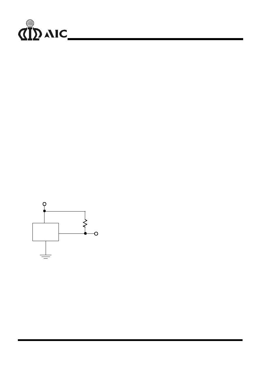
TYPICAL APPLICATION CIRCUIT
100K
AIC1680N
V
OUT
V
IN
VOUT
GND
VDD
Voltage Level Indicator (N-ch Open-Drain Output)
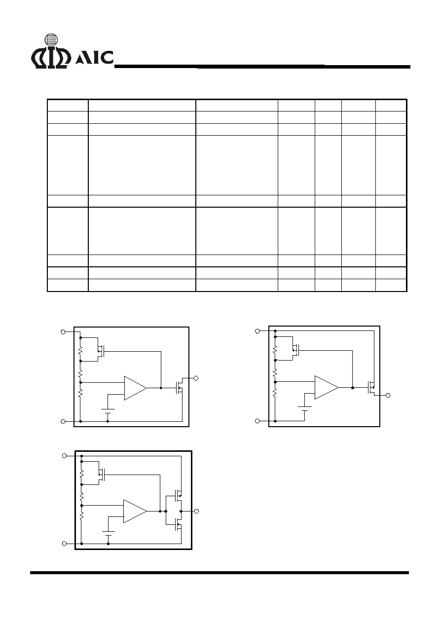
DESCRIPTION
The AIC1680 is an accurate, ultra-low power
consumption voltage detector IC, fabricated with
advanced CMOS process. The AIC1680 con-
sists of a comparator, a voltage reference unit,
a resistor divider, two output drivers, and a
hysteresis circuit.
The consumption current is so low that it can
often be ignored when compared to the battery
self-discharge current. The values of detection
and hysteresis voltage are set internally and are
accurately controlled by trimming techniques.
There are three types of output: N-ch open-
drain, P-ch open-drain, and CMOS. Four types
of package, TO-92, SOT-89, SOT-23 and SOT-
23-5, are available to save board space.

AIC1680
2
ORDERING
INFORMATION
ORDER NUMBER
AIC1680CU
(SOT-23)
PIN CONFIGURATION
FRONT VIEW
1: VOUT
2: VDD
3: GND
1
2
3
1
2
3
PACKAGING TYPE
U: SOT-23
X: SOT-89
Z: TO-92
V:SOT23-5
AIC1680CZ
(TO-92)
FRONT VIEW
1: VOUT
2: VDD
3: GND
DETECTION VOLTAGE OPTIONAL
16: 1.6V
17: 1.7V
:
:
60: 6.0V
OUTPUT TYPE
N: N-ch Open Drain
P: P-ch Open Drain
C: CMOS
AIC1680XXXCX
AIC1680CX
(SOT-89)
1
2
3
FRONT VIEW
1: VOUT
2: VDD
3: GND
1
4
5
(MARK SIDE)
FRONT VIEW
1: VOUT
2: VDD
3: GND
4: NC
5: NC
AIC1680CV
(SOT-23-5)
2
3
ABSOLUTE MAXIMUM RATINS
Supply Voltage ........................................................................................................ 10V
Output Voltage ................................................................................Vss-0.3 to 10V
Operating Temperature Range .................................................................. -30
∞C ~ 80∞C
Storage Temperature Range ................................................................... - 65
∞C ~ 150∞C
Lead Temperature (Soldering) 10 sec. ...................................................................260
∞C
Output Current .................................................................................................20mA
AIC1680
4
PIN DESCRIPTIONS
V
DD
: Power Supply and Detected Voltage Input.
GND: Ground.
Vout: Detector Output
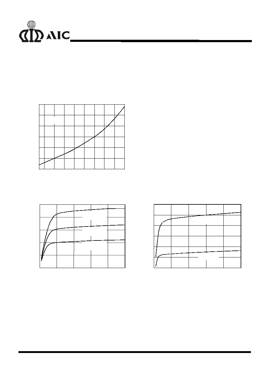
TYPICAL PERFORMANCE CHARACTERISTICS
2
3
4
5
6
7
8
9
10
0.5
1.0
1.5
2.0
2.5
3.0
3.5
Ta=25
∞C
Supply Current vs. Supply Voltage
S
upp
l
y
C
u
rr
e
n
t (
µ
A)
Supply Voltage(V)
N-ch Driver Sinking Current vs. V
DS
0
1
2
3
4
5
0
1
2
3
4
5
V
DET
=1.8V
V
DD
=1.3V
V
DD
=1.5V
V
DD
=1.7V
S
in
k
i
n
g
Cu
rr
e
n
t
(
mA
)
V
DS
(V)
V
DET
=1.8V
Si
nk
i
n
g C
u
r
r
ent
(
m
A)
V
DS
(V)
0
1
2
3
4
5
0.2
0.4
0.6
0.8
1.0
1.2
1.4
V
DD
=1.1V
V
DD
=0.9V