AIC1714
Negative Voltage Regulator
Analog Integrations Corporation
4F, 9 Industry E. 9th Rd, Science-Based Industrial Park, Hsinchu, Taiwan
DS-1714-03 012102
TEL: 886-3-5772500
FAX: 886-3-5772510
www.analog.com.tw
1
n
FEATURES
l
Low Power Consumption.
l
Low Temperature Coefficient.
l
Output Short Circuit Protected.
l
Wide Operating Voltage Range.
l
Good Input Stability.
l
Space-Saving Package:
TO-92
or
SOT-89
n
APPLICATIONS
l
LCD for Printing Calculators
l
Cameras
l
Voltage References for Instrumentation
n
DESCRIPTION
The AIC1714 is a series of 3-terminal negative
voltage regulators with output voltages
internally set below the positive supply voltage.
Since the AIC1714 consumes less current and
only requires a small input/output voltage
difference than existing industry standard 3-
terminal voltage regulators, a battery-powered
portable equipment is afforded a high capacity
and longer service life. The AIC1714 is ideal for
power source of liquid crystal displays.
n
TYPICAL APPLICATION CIRCUIT
AIC1714-33
GND
OUT
VIN
+
1
�
F
-3.3V
-6V
C1
Negative Voltage Regulator
n
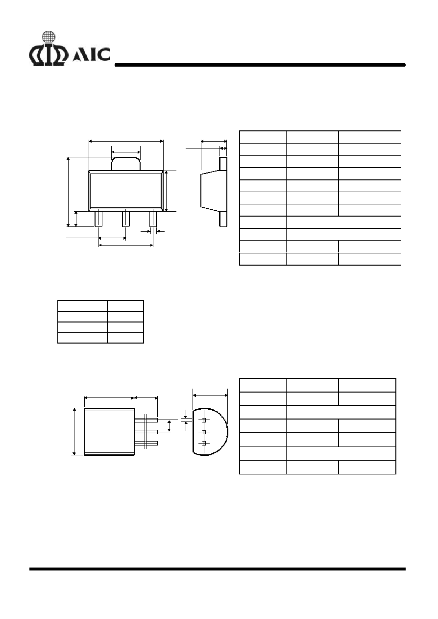
ORDERING INFORMATION
SOT-89
TOP VIEW
1. VIN
2. GND
3. VOUT
1
2
3
1
2
3
PACKING TYPE
TR: TAPE & REEL
TB: TUBE
PACKAGE TYPE
X: SOT-89
Z: TO-92
OUTPUT VOLTAGE
30: -3.0V
33: -3.3V
50: -5.0V
AIC1714-XXCXXX
Example: AIC1714-30CXTR
�
-3.0V Version, in SOT-89 Package
& Tape & Reel Packing Type
PIN CONFIGURATION
TO-92
TOP VIEW
1. VIN
2. GND
3. VOUT
AIC1714
2
n
ABSOLUTE MAXIMUM RATINGS
Supply Voltage
.....................
............................... ... ... ................................
-13V
Operating Temperature Range
............................ ... ... ........................
- 20
�
C~80
�
C
Storage Temperature Range
........................... ... ... .........................
- 65
�
C~150
�
C
Power Dissipation
SOT-89 Package
........ ..............
0. 80W
TO-92 Package
........... ............
0.78W
n
TEST CIRCUIT
V
OUT
A
A
V
V
+
LOAD
GND
VIN
OUT
AIC1714
+
+
_
Voltage
Source
+
I
OUT
I
IN
V
IN
1
�
F
-
n
ELECTRICAL CHARACTERISTICS
(V
IN
= -6.0V, T
J
=25
�
C, unless otherwise
specified.)
PARAMETER
TEST CONDITIONS
SYMBOL
MIN.
TYP.
MAX.
UNIT
AIC1714-30
-2.95
-3.0
-3.05
V
AIC1714-33
-3.25
-3.3
-3.35
V
Output Voltage
I
OUT
=300
�
A
AIC1714-50
V
OUT
-4.93
-5.0
-5.07
V
Load Regulation
I
OUT
=0~5mA
V
OUT
20
100
mV
I/O Voltage Difference
I
OUT
=300
�
A
V
DIFF
50
200
mV
Supply Current
I
OUT
= 0
I
IN
6
12
�
A
Input Stability
V
V
V
OUT
IN
OUT
�
0.05
%/ V
Temperature Coefficient
-25
�
C~85
�
C
T
C
50
ppm
Output Short Circuit Current
R
LOAD
=0
15
24
mA
AIC1714
3
n
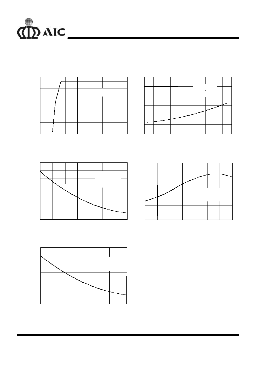
TYPICAL PERFORMANCE CHARACTERISTICS
Fig. 1 Output Voltage vs. Supply Voltage
(Load Current=300
�
A)
Output Voltage (V)
Supply Voltage (V)
0
-2
-4
-6
-8
-10
-12
-14
-1.0
-1.5
-2.0
-2.5
-3.0
-3.5
T
A
=25
�
C
Supply Voltage (V)
Supply Current Voltage vs. Supply Voltage
(No Load)
Supply Current (
�
A)
-4
-6
-8
-10
-12
4
5
6
7
8
9
10
AIC1714-33
T
A
=25
�
C
Supply Current (
�
A)
-40
-20
0
20
40
60
80
100
4.4
4.6
4.8
5.0
5.2
5.4
5.6
5.8
Fig. 3 Supply Current vs Temperature
Temperature (
�
C)
AIC1714-33
V
IN
= -6V
I
OUT
=0
Fig 4 Output Voltage vs Temperature
Output
Voltage(V)
Temperature (
�
C)
-40
-20
0
20
40
60
80
100
-3.26
-3.27
-3.28
-3.29
-3.30
V
IN
= -6V
I
OUT
=300
�
A
Fig. 5 Output Voltage vs Load Current
Output Voltage (V)
Load Current (mA)
0
1
2
3
4
5
-3.255
-3.260
-3.265
-3.270
-3.275
V
IN
= -6V
T
A
=25
�
C

AIC1714
4
n
BLOCK DIAGRAM
+
VOUT
VIN
GND
-
+
-
V
REF
n
PIN DESCRIPTIONS
VOUT PIN - Output pin.
GND PIN - Power GND.
VIN PIN
- Power Supply Input.
n
APPLICATION INFORMATIONS
A 1
�
F (or greater) capacitor is required between
the AIC1714 output and ground for stability.
Without this capacitor the part will oscillate. Even
though most types of capacitor may work, the
equivalent series resistance (ESR) should be held
to 5
or less if Aluminum electrolytic type is used.
Many Aluminum electrolytic have electrolytes that
freeze at about -30
�
C, so solid tantalums are
recommended for operation below -25
�
C. The
value of this capacitor may be increased without
limit.
A 0.1
�
F capacitor (or greater) should be placed
from the AIC1714 input to ground if the lead
inductance between the input and power source
exceeds 500nH (approximately 10 inches of trace).